Note : Les descriptions sont présentées dans la langue officielle dans laquelle elles ont été soumises.
2085117
Power Am pl if ier
Field of the Invention
This invention generally relates to power amplifiers,
and more specifically to improvements in the power
10 control range and Amplitude Modulated (AM) output of the
power amplifier.
Background of the Invention
The use of power amplifiers for transmitting radio
frequency signals has many applications, including, but
not limited to, radiotelephone communications systems.
When using a power amplifier in a radiotelephone certain
qualities of the power amplifier are desirable including:
20 1) a large power control range, 2) temperature stability,
3) efficient use of current, and 4) minimal AM output.
A total power control range is limited on the high end
by the gain of the amplifier at the maximum bias current
and the power control range is limited on the low~nd by
2 5 the isolation of the amplifier from the radio freq~ency
(RF) input when the bias current is zero. Within this
range,the output power is approximately proportional to
the square of the bias current.
Typically, in order to obtain maximum gain and
30 efficiency for a given bias current, class C amplifiers
2085 1 1 7
are used. In previous class C amplifier configurations, the
isolation from the RF input, in absence of bias current, was
limited to the parasitic capacitance between the collector and
the base of the transistor.
Brief Description of the Drawings
FIG. 1 is a block diagram of a radiotelephone
communications system which may employ the present
nvention .
FIG. 2 is a block diagram of a power amplifier and
corresponding power amplifier control circuitry which may
employ the present invention.
FIG. 3 is a power amplifier control circuit which is
contained in the prior art.
FIG. 4 is a two-stage power amplifier circuit which may
employ the present invention.
FIG. 5 is a control characteristic and an AM
characteristic of a power amplifier which may be contained in
prior art.
FIG. 6 is a control characteristic and an AM
characteristic of a power amplifier which may be a result of
the present invention.
FIG. 7 is the GSM time mask as defined by GSM
recommendation 05.05 (4.2.2).
FIG. 8 is the GSM spectral frequency mask as defined
by GSM recommendation 05.05 (4.5.2).
In order to obtain the desired temperature stability in low
efficiency amplifiers, a resistor is coupled between the emitter
,~
3 20851 17
of the transistor contained within the amplifier to ground.
This resistor stabilizes the amplifier over temperature,
however, it is undesirable because it lowers the efficiency of
the amplifier. In order to obtain high efficiency of the
amplifier, the collector and emitter must be void of any lossy
resistive elements. Removal of these lossy elements
increases the potential gain and efficiency of the amplifier,
however, it causes the amplifier circuit to be extremely
temperature sensitive, unless other bias stabilization measures
are employed.
FIG. 3 illustrates a commonly employed circuit topology
for RF power amplifiers. The focus of the circuit is the bipolar
transistor 309 in a common emitter configuration. This circuit
attempts to attain bias control and temperature stability by
using the clamping diode 305. The intrinsic characteristics of
this clamping diode 305 are matched to the base emitter
junction of the transistor 309. The diode voltage tends to
track the base to emitter voltage of the transistor 309
resulting in a temperature stable bias current which is
approximately proportional to the control voltage 301. The
clamping diode 305 also serves as a circuit protector from
excessive control voltage 301.
The amplifier of FIG.3 would have a typical control
characteristic and AM characteristic as illustrated in FIG.5.
The control characteristic is a plot of the RF output power
501 over the control voltage range 301. The AM
characteristic is a plot of percentage AM output 503 for one
4 20851 1 7
percent AM input on the RF input signal over the control
voltage range 301. The peak of the AM characteristic 503
tends to be aligned with the steep portion of the control
characteristic 501.
If two amplifiers as shown in FIG.3 are cascaded and
the control voltage inputs are tied directly together, then the
composite control characteristic would have approximately
twice the slope of the individual control characteristic 501.
The magnitude of the AM characteristic would be
approximately double the individual AM characteristic 503.
The increased AM characteristic is undesirable, because the
AM modulation would result in power fluctuations on the RF
output signal 313.
The lossy elements were not present in this circuit, thus,
allowing for a maximum potential gain and efficiency of the
amplifier. However, the isolation of the RF signal from the
amplifier in absence of bias current is dependent on the
parasitic capacitance of the transistor 309. Thus, the power
control range is not maximized.
Therefore, there is a need for a temperature stable,
power efficient RF power amplifier having a large power
control range, and minimal AM output.
Summary of the Invention
The present invention encompasses an amplifier which
includes a first input signal, a first output signal, a bias
current and a control voltage. The first signal carries a first
radio frequency signal. The first output signal carries an
20851 17
amplified first radio frequency signal. Variances in the bias
current are responsive to variances in the control voltage.
The amplifier has means for amplifying the first input signal.
The amplifier also has means for stabilizing the bias current
responsive to changes in temperature and means for
attenuating the first radio frequency signal responsive to
changes in the control voltage contained within the same
element.
, .~
2~8511~
Description of a Preferred Embodiment
The invention disclosed herein, may be employed in a
TDMA radiotelephone system which is illustrated in FIG.
1. In a radiotelephone system there is a fixed site
transceiver 101, which sends out RF signals to portable
and mobile radiotelephones contained within a
geographic coverage area. One such phone is the portable
radiotelephone 103. A radiotelephone system is assigned
a frequency band which it is allowed to broadcast within.
The frequency band is broken up into several channels
200 Kilohertz wide. Each channel is capable of handling
communications between the transceiver 101 and up to 8
radiotelephones within its coverage area. Each
radiotelephone is assigned time slots in which to
broadcast and receive information from the transceiver
101. Each time slot is approximately 577 microseconds
in duration. Portable radiotelephone 103, model number
F19UVD0960AA available from Motorola, Inc., includes a
transmitter 107, a receiver 109, and a digital signal
processor (DSP) 111, such as the DSP 56000 available
from Motorola, Inc. Several signals are transmitted
between the DSP 111 and-the transmitter 107 on--
2 5 multiple signal lines 113. ~
The transmitter 107 and the transceiver 101 both
contain power amplifiers with stringent requirements as
defined by the Group Special Mobile (GSM)
recommendations ETSI/PT-12 05.05 (4.2.2 and 4.5.2),
3 0 March, 1991. The specifications require any transmitter
-
2~85117
to meet a time mask as shown in FIG.7 and a spectral
frequency mask as shown in FIG.8.
The antenna 105 is used to transmit and receive radio
frequency signals to and from transceiver 101. Upon
5 receiving signals, the antenna 105 converts the signals
into electrical radio frequency signals and transfers the
signals to the receiver 109. The receiver 109
demodulates and converts electrical radio frequency
signals into data signals usable by the rest of the
10 portable radiotelephone 1 03.
Upon transmission of the radio frequency signals, the
DSP 111 feeds the transmitter 107 information which is
desired to be transmitted and also controlling
information for the transmitter 107 via signal lines 113.
15 The transmitter 107 takes the data and converts it into
electrical radio frequency signals and gives the
electrical radio frequency signals the appropriate
amount of power necessary with use of the power
amplifier. The antenna 105 then takes the electrical
20 radio frequency signals and converts them into radio
frequency signals and transmits them into the air for use
by the transceiver 10 1.
The power amplifier 203 and its associated
controllers are located in - the transmitter 107, a~d
25 illustrated in the block diagram of FIG. 2. The f~rnction
of the power amplifier 203 is to take in the radio
frequency input which contains voice and data which is
to be transmitted back to the fixed site transceiver 101
and amplify the RF input signals 209 to the appropriate
30 power level for transmission. The exciter 205 is an
-
20851 17
adjustable power amplifier which adjusts the RF input signals 209
to their proper input level for the power amplifier 203.
The block diagram of FIG. 2 contains several control loops,
including the standard control loop, the ramp up loop, and the
saturation detector loop of the power amplifiers. The details of the
power ramp up loop may be found in Canadian Patent Application
No. 2,086,673 "Power Amplifier Ramp Up Method and
Apparatus", filed on behalf of Hietala et al., on May 8, 1992
assigned to the assignee of the present invention. The details of
the saturation detector loop may be found in Canadian Patent
Application No.2,086,541 "Power Amplifier Saturation Detection
and Correction Method and Apparatus", filed on behalf of Black et
al., on May 8, 1992 assigned to the assignee of the present
invention.
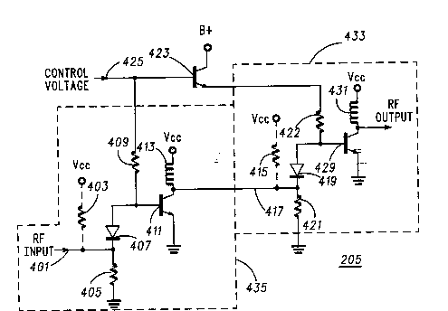
The circuit in FIG. 4 is a two-stage power amplifier with
variable gain used as the exciter 205. The first stage of
amplification 435 includes: the transistor 411, the diode 407, the
inductor 413, the resistors 403, 405, 409. The second
amplification stage 433 includes: the transistor 429, the diode
419, the inductor 431, the resistors 415, 421, 422. The two
amplification stages are directly coupled together via signal line
417.
The control voltage 425 is used to control the bias current
in both amplification stages 433, 435. The control voltage is
serialized such that it can control the gain of both amplifier stages
433, 435 simultaneously. The transistor 423 is located on the
control voltage line 425 between the two amplification stages.
The purpose
~,,.
2Q8511 7
of the transistor 423 is to shift the voltage of the
control voltage signal 425, separating the control
characteristic of the first amplification stage relative
to the second amplification stage, resulting in a control
5 characteristic 601 of FIG. 6. Other equally efficient
ways of shifting the voltage are available including
diodes or voltage divider circuits. The difference in the
control voltage 425 for the amplification stages
433,435 is also used to separate the two power
1 0 amplifier stages 433,435 from the region in the AM
characteristic which contains highest AM output. In the
preferred embodiment, the circuit illustrated in FIG. 4
had AM output less than 2% over the entire power output
range for 1% of AM input on the RF input signal 401. This
1 5 results in an AM characteristic resembling the waveform
603 in FIG.6. Without the shifting of the control voltage
signal 425, the magnitude of the AM characteristic
would be approximately twice as large at the peak. This
would potentially violate the maximum power output
2 0 required in the GSM spectral time mask illustrated in
FIG.7.
The transistors 411 and 429 are set up for high
power efficiency. The emitter and collector of the
transistors are void of an-y lossy elements, allow*ng for
2 5 maximum efficiency. The ~ emitter of both transls-tors
411 and 429 are tied directly to electrical ground, and
the collectors are tied to a supply voltage through
inductor 413 and inductor 431 respectively. The
inductors 413, 431 serve as an RF load for the amplifier.
3 0 Connecting the emitters directly to ground prevents any
2085117
unnecessary loss of amplification, but leaves the
amplifier temperature unstable.
The diodes 407, 419 stabilize the bias current over
temperature, isolate the amplifier from the RF input
signal 401 in absence of a control voltage 425 and
provide circuit protection from excessive control
voltage 425. First, the diode serves as a bias stabilizer.
By matching the diode 407 with the base emitter
characteristics of transistor 411, the bias current
1 0 through the transistor will be stable over temperature
for a given control voltage 425, as long as resistor 405
remains small. Secondly, the diode 407 acts to isolate
the RF input signal 401 from the transistor 411 in
absence of a control voltage 425. As the control voltage
1 5 increases the conductivity of diode 407 increases, thus,
the RF input signal is unattenuated while there is an
active control voltage and current flowing through diode
407. In the absence of the control voltage 425, the
conductivity of diode 407 is low, isolating the RF input
2 0 signal 401 from the remainder of the amplifier circuitry.
Therefore, the amplifier stage has high input to output
isolation in the absence of a control voltage signal
giving the amplifier stage a larger power control range.
Third, the diode 407 acts as a protector against--
2 5 excessive control voltage~~signals. --~
Resistor 405 serves as a DC return element to the
diode 407 and as a RF blocking element. Its value should
be chosen to match the emitter ballasting voltage drop
internal to the transistor 411. The pull-up resistor 403
is used to provide reverse bias current on the diode in
1 1 2Dg51I7
absence of control voltage 425, thereby, further
decreasing the conductance of diode 407 and increasing
the attenuation of the RF input signal 401. This resistor
403 is optional, not necessary to have a successful
5 amplifier circuit.
The two amplification stages are DC coupled together
allowing for maximum power from the first amplifier
stage to be coupled into the second amplifier stage.
Thus, the circuit illustrated in FIG. 4 is a
10 temperature stable, power efficient RF amplifier design
with a large power control range and improved AM
output.
What is claimed is: