Note : Les descriptions sont présentées dans la langue officielle dans laquelle elles ont été soumises.
73
1
Power Amplifier Ramp Up Method and Apparatus
Field oF the Invention
Generally, this invention relates to power amplifier
control circuits. More specifically, the invention relates
to power ramp up control circuits for power amplifiers.
1 0
Backsround of the Invention
The use of power amplifiers in transmitting radio
15 frequencies (RF) signals has many applications, including
but not limited to radiotelephone communications
systems. In a radiotelephone communications system,
there are multiple fixed site l,dnsceivers. Each fixed
site transceiver is an interface between the line
2 0 telephone system and multiple, portable, or mobile
radiotelephone systems contained within a geographic
area served by the fixed site transceiver. The fixed site
transceiver and the radiotelephone communicate by
sending and receiving FM moduiated radio frequency
25 signals to each other. _
In an analog radiotelephone system, there is a large
available RF spectrum available for radiotelephone
communications. The available RF spectrum is
channelized into relatively narrow segments of
30 frequency. Upon request, each ,ddiol~'aphone is
allocated a frequency channel upon which to broadcast
and receive information from the fixed site transceiver.
This is known as a Frequency Division Multiple Access
2~8~73
2
(FDMA) system. During a phone call, the rd~t~ ,phone
transmitter would turn-on and remain on the fixed
frequency for the entire time of the phone call. Thus, the
L,dl~s",ilLtJr and subsequently the power amplifier (PA)
5 of the radiotelephone only needed to turn-on once and
turn-off once for a given phone call which could last
several minutes. The fixed site transceiver could also
remain on for the duration of a phone call. In an FDMA
system, since there are a limited number of turn-ons,
10 the turn-on and turn-off requirements of the power
amplifier are not very stringent. If a L,dns",iLLer is
turned on quickly, there is a momentary large burst of
noise, however, since this would only occur once during a
conversation, it would not substantively affect the
15 communication system. Similarly, if the power
amplifier is turned on slowly, there would be an
imperceptible gap in the conversation at the beginning of
a phone call. These problems are only inconveniences to
the user and are not substantive system degrading
2 0 problems.
In the newly proposed digital cellular radiotelephone
systems, the power amplifier turn-on requirements have
increased dramatically. The new systems use a time
division multiple access (TDMA) communications system.
25 In a TDMA communications system, 8 or 16
radiotelephones share a stngle 2ûO kilohertz wide- - -
channel on which to broadcast. Each radiotelephone in a
channel is allocated one 577 microsecond (uS) time slot
on a repetitive basis. During this time slot the
30 radiotelephone ramps up the power amplifier to the
proper frequency and power, sends the desired data, and
ramps down the power amplifier so as not to disturb or
interfere with the other users sharing the same
2~8~67~
frequency. Thus, the requirements for controlling the
power amplifier are greatly increased.
The Group Special Mobile (GSM) lec~l"",enclalions
ETSIIPT-12 05.05 (4.2.2 and 4.5.2), March, 1991 were
5 developed to define a digital radiotelephone
communications system. These recommendations were
aware of the increased power amplifier requirements
and have defined a time mask arld a spectral frequency
mask, as illustrated in FIGS. 7 and 8, which all
10 radiotelephone equipment used in the system must meet.
The specifications concernins the time and frequency
masks demand the development of a very smooth ramp up
of the PA and stringent time cor,~l,di"~
Without these requirements, TDMA digital
15 communications systems would not operate. If the PA is
turned on too slow, even a few ~iu~useconds, seYere
damage to the data l,dnsl"i~L~d between the fixed site
~Idl1sceiv~r and the rd~iot~l~phone would occur. Turning
a power amplifier on very quickly results in large
2 0 spectrum burst causing interference with
radiotelephones of the same or similar frequencies.
Therefore, a power amplifier controller is needed which
ramps the power amplifier up to the required power
quickly and smoothly without causing a frequency noise
2 5 burst or missing data. _
Previously, a digital signal processor (DSP) has~been - -
used along with a di~ital-to-analog converter (D/A)to
generate a ramp up of the PA as required by the GSM
specifications. The Automatic Output Control (AOC)
30 voltage generated by the DSP is fed into an integrator
where it is compared to the output of an RF power
detector. The difference between the AOC signal and the
detector sisnal is fed into the control input of the power
~ 4 2~8~
amplifier system. Under ideal conditions, this closed
loop power amplifier system will adjust the control
voltage until the RF control detector is equal to the AOC
voltage. However, the system is far from ideal.
Two characteristics of the system lead to shortfalls
in maintaining the time and spectral frequency masks.
First, the detector has a finite range over which it
detects RF from the output of the amplifier. Below this
range, the detector outputs a small voltage, which does
not correlate to the power changes of the amplifier.
Under this condition, the control loop is open and the
output power is in no way correlated to the AOC voltage.
In fact, the i"leyrdLur will force its output to the
maximum negative voltage, because the detector voltage
will be greater than the AOC voltage. Secondly, the
exciter/power amplifier typically has a turn-on
threshold which the i"ley,dlor must meet before the
ramp up waveform can be input to the amplifier.
Because of the shortfalls of the control loop, when
the power amplifier becomes active, and the detector
sllhsequently becomes active, the control loop closes and
attempts to track the AOC voltage. At this point,the
control loop will attempt to track the AOC voltage at its
current level. This will result in a spectral frequency
mask violation becausa of the sharp turn-on of the=power
amplifier 401 as shown in FIG. 4.
Therefore, a need exists for a power amplifier
control loop which is adaptive to the requirements of
each individual power amplifier and allows for a quick
3 0 and smooth power ramp up.
_ Summary of the Invention
5 2~8~7~
The present invention encompasses a transmitter
including means for amplifiying a first signal and means
for c~llll.,lii.lg the means for amplifying. The means for
amplifying having at least two inputs, at least one
5 output, an active state and an inactive state and
responsive to a voltage of a second signal. The first
signal having a power level, a first frequency and
coupled to a first one of the at least two inputs of the
means for amplifying.
The means for controlling comprises: 1) means for
generdli"g the second signal coupled to a second one of
the at least two inputs of the means for amplifying; 2)
means for generating a third signal which is responsive
to the active state of the means for amplifying; 3)
15 means for determining the voltage level of the second
signal, dependent on the state of the third signal,
whereby, the means for amplifying the first signal is
ramped up into the active state without a substantial
- burst of frequency noise.
Brief Description of the Drawings
FIG. 1 is a block diagram of a ,d~io~ phone
communications system in accordance with the present
25 invention.
FIG. 2 is a block diagram of a power amplifier-and
corresponding p~wer amplifier control circuit in
accordance with the present invention.
FIG. 3 is a power versus time graph from the output
30 of a power amplifier described in the Background of the
Invention.
FIG. 4 is a power versus time graph which shows the
desired output of a power amplifier and the waveform of
6 2~ 7~
a power amplifier which does not employ the present
invention.
FIG. 5 is a power versus time graph of a power
amplifier control loop described in the Background of the
5 Invention.
FIG. 6A is a schematic of a power amplifier control
circuit in accordance with the present invention.
FIG. 6B is a schematic diagram of an alternative
embodiment in accordance with the present invention.
FIG. 7 is ths GSM time mask as defined by GSM
recommendation 05.05 (4.2.2).
FIG. 8 is the GSM spectrai frequency mask as defined
by GSM ,~co,,,,,,el-ddliùn 05.05 (4.5.2).
Description of a Preferred Embodiment
The invention disclosed herein, may be employed in a
TDMA-radiotelephone system which is illustrated in FIG.
1. In a ,ddiot~'~pl1one system there is a fixed site
20 L,dnsceiver 101, which sends out RF signals to portable
and mobile radiotelephones contained within a
geographic coverage area. One such phone is the portable
radiotelephone 1û3. A radiotelephone system is assigned
a frequency band which it is allowed to broadcast within.
25 The frequency band is brok~n up into several chanrlels
200 Kilohertz wide. Each ~hannel is capable of ha~dling
communications between the lldl1sC~iv~r 101 and up to 8
radiotelephones within its coverage area. Each
radiotelephone is assigned time slots in which to
3 0 broadcast and receive information from the transceiver
101. Each time slot is approximately 577 ~ useconds
in duration. Portable radiotelephone 103 model number
F1 9UVD0960AA available from Motorola Inc. includes a
7 2~86~
^
lldns",il~er 107, a receiver 109, and a digital signal
p~ocessor (DSP) 111, such as the DSP 56000 available
from Motorola, Inc. Several signals are transmitted
between the DSP 111 and the L,dns",iLL~r 107 on
5 multiple signal lines 113.
The transmitter 107 and the transceiver 101 both
contain power arnplifiers with stringent requirements as
defined by the Group Special Mobile (GSM)
recommendations ETSI/PT-12 05.05 (4.2.2 and 4.5.2),
10 March, 1 991 . The specifications require any transmitter
to meet a time mask as shown in FIG.7 and a spectral
frequency mask as shown in FIG.8. The antenna 105 is
used to transmit and receive radio frequency signals to
and from L,dnsceivcr 101.
Upon receiving signals, an antenna 105 converts the
signals into electrical radio frequency signals and
transfers the signals to the receiver 109. The receiver
109 demodulates and converts electrical radio frequency
signals into data signals usable by the rest of the
2 0 portable radiotelephone 103.
Upon transmission of the radio frequency signals, the
DSP 111 feeds the transmitter 107 information which is
desired to be transmitted and also controlling
information for the L,dl1s,l,ilLer 107 via signal lines 113.
25 The transmitter 107 takes the data and converts 4 into
electrical radio frequency signals and gives the -- -
electrical radio frequency signals the appropriate
amount of power necessary with use of the power
amplifier. The antenna 105 then takes the electrical
30 radio frequency signals and converts them into radio
frequency signals and transmits them into the air for use
by the transceiver 101.
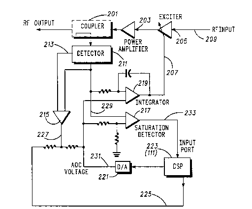
The power amplifier 203 and its ~soci~t~d controllers
are located in the l,dnsr"iLIdr 107, and illustrated in the
block diagram of FIG. 2. The function of the power
amplifier 203 is to take in the radio frequency input
5 which contains voice and data which is to be transmitted
back to the fixed site transceiver 101 and amplify the RF
input signals to the appropriate power leYel for
transmission. The exciter 205 is an adjustable power
amplifier which adjusts the RF input sisnals 209 to their
10 proper input level for the power amplifier 203.
The block diagram of FIG.2 contains several control
loops, including the standard control loop, the ramp up
loop, and the saturation detector loop of the power
amplifiers. All of the control loops utilize the coupler
201. The coupler 201 is an electromagnetic coupler
which couples the RF output signals into the control
loops without causing excessive loss to the RF output
signals.
The detector 211 detects the forward power level of
the RF output signals and creates a power level signal
229 the voltage of which is responsive to the amount of
forward power in the RF output signals. The detector
211 also outputs a reference signal 213. The voltage of
the reference signal 213 is responsive to the DC offset
output by the detector in absence of activity of th~
power amplifier 203.
The power amplifier control loop utilizes the
comparator 215 and the DSP 223 in addition to the
- standard control loop. The comparator 215 outputs the
signal 227. The output signal 227 indicates detection of
activity of the power amplifier 203 and the exciter 205.
The output signal 225 is generated by the DSP 223 and
used to pull up the output signal 227. The output signal
2~
~' 9
225 is high at the beginning of a timeslot and is lowered
after the desired output waveform 505 is output by the
DSP 223. This causes the output signal 227 to be high
during an active time slot and before the power
amplifier 203 and the exciter 205 become active. Upon
activation of the power amplifier 203 and the exciter
205, the output signal 227 becomes low.
10 uS into an active timeslot, the DSP 223 generates
a desired waveform and sends it to the digital-to-analog
converter 221. In this preferred embodiment, the
preferred waveform 505 is a raised cosine which ramps
the power amplifier 203 smoothly up to its desired
power level. The D/A converter 221 converts the digital
input to an analog output signal 231, known as the AOC
signal. The AOC signal 231 is then put into the
integrator 219, the output signal 207 of the integrator
219 is input as a control voltage to the exciter amplifier
205 to control the amplification level of the exciter 205.
An illustration of the voltage of the AOC signal 231
is shown in FIG. 5. Initially, the DSP 223 and thus the
D/A 221 in conjunction with output signal 227 output a
constant DC voltage 501 on the AOC signal 231, thus, the
integrator puts out a constant slope signal shown in 503.
This signal 503 is output until the comparator 215
2 5 detects activity of the power amplifier 203. UporL
detection of activity of the- power amplifier 203,-the
output signal 227 is reduced to ground, which effectively
stops the linear ramp-up. The AOC signal 231 remains at
a voltage sufficient to maintain activity of the power
amplifier 203 until the DSP 223 puts out the desired
waveform to ramp the exciter and power amplifier into
their desired power level. In the preferred embodiment,
the delay is 10 uS from the beginning of the timeslot and
` ~ lo 2~8~7~
the desired waveform is a raised cosine wave 505 as
shown in FIG.5.
The saturation control loop prevents the exciter 205
and power amplifier 203 from vxceedi~,~ beyonds their
S amplification limit because of the control signal input
207. The saturation loop consists of coupler 201, the
detector 211, the comparator 217 and the digital signal
processor 223. The saturation detection comparator 217
compares the detector output signal 229 to the voltage
10 of the AOC signal 231 to determine if the detector
output signal 229 is (~spol1siv~ to changes in the voltage
of the AOC signal 231. This comparison will indicate
saturation from the control voltage when the voltage oF
the detector output signal 229 drops below the voltage
15 of the AOC signal 231, because the detector voltage will
not change with a corresponding change in the voltage of
the AOC signal 231 during saturation. The saturation
comparator output signal 233 is input into the DSP 223
- which contains an algorithm. The algorithm steps down
20 the voltage of the AOC signal 231 until there is a change
in the detector output voltage 229. Then, the voltage of
the AOC signal 231 can be stepped up or down. In the
preferred embodiment, the voltage of the AOC signal 231
is stepped down further to insure that the power
2 5 amplifier 203 remains unsaturated, however, the voltage
of the AOC signal 231 coul~ be stepped up to becom~ - -
closer to the saturation threshold depending on the
specific needs of a given implementation. The voltage of
the AOC signal 231 is held at a level slightly below the
30 saturation threshold until the end of the time slot. For
further details concerning the saturation control loop
refer to U.S. Patent Application No. 07/709,737 entitled
~Power Amplifier Saturation Detection and Correction
6 7~
Method and Apparatus", filed on behalf of Black et al., on
June 3, 1991 assigned to the assisnee of the present
invention.
FIG. 6A illustrates the circuit diagram of a preferred
5 embodiment of the ramp up controller. In this preferred
e", odil"er,L, the col"pa,dlur output signal 613 is coupled
through resistor 627 to the AOC signal 625. If the
output of the c~l"pa,dLur 615 is open, thus signifying a
non-active PA, and the DSP 223 is providing 5 volts to
10 resistor 617 as a pull-up on the open collector output of
the comparator 615, then the ramp up signal is provided
on the AOC signal 625 by the voltage division of resistor
629, and resistor 617. When the power amplifier 2û3
becomes active, the c~l,,pa,dLur output signal 613 will
15 go low and clamp the junction of resistor 627 and
resistor 617 to ground, thus,~ii",ir,dLi"g the DC pulse.
After 1û uS has passed from the beginning of a timeslot,
the DSP 223 and D/A converter 221 outputs the desired
waveform on the AOC signal 625. Once the DSP 223 has
20 fed the AOC signal 625 with its desired waveform, which
in a preferred embodiment is a raised cosine 5û5,
resistor 617 must be pulled low to avoid the up ramp
during a non-active transmitter time.
FIG. 6B reveals an alternative circuit diagram of the
25 ramp up controller. The comparator output signal=613 is
coupled to the DSP 223 and is indirectly coupled back to
the AOC signal 625. The signal 613 which returns to the
DSP 223 is used to notify the DSP 223 when the power
amplifier 2û3 has entered its active state. The problem
30 of controlling the output to avoid a surge in the exciter
power because of the turn on threshold is illustrated by
waveform 3û3. This problem is caused by the intrinsic
delay in the DSP 223 behveen receiving the comparator
12 2~8~;6~
output signal 223 and subsequently controlling or
limiting the AOC signal 625, therefore, a real time
circuit was developed. This circuit is the indirect
coupling between the c~ll,,oar~l~r output signal 613 and
5 the AOC signal 625. This circuitry immediately clamps
the voltage of the AOC signal 625 to ground upon
detection of activity in the power amplifier 203 to avoid
the overshoot as.illustrated in waveform 401. Upon
detection, the co~ ,a,dLor output signal 613 grounds the
10 capacitor 631, in the preferred embodiment capacitor
631 has a value of 47 pf. While the capacitor 631 is
discharging, it will pull the base of transistor 623 down
and thus, saturate transistor 623 until capacitor 631 is
discharged. In the preferred embodiment, the resistor
619 and resistor 621 have values of 100 kohms and 220
kohms respectively. Transistor 623 in the preferred
el"L~o.Jil"e"~ may be an MMBT 3640 available from
Motorola, inc. By saturating the transistor for that
amount of time, the voltage of the AOC signal 625 is
20 pulled to ground, maintaining the power amplifier 203 at
its turn on threshold until the DSP 223 has time to react.
The DSP 223 and D/A converter 221 generates the
desired ramp up waveform on the AOC signal 625. In the
preferred e,llLJodil"ent the desired waveform is a raised
25 cosine 505 as shown in FIG. 5.
With the implementation of the up ramp contro~ loop
a class C amplifier may be smoothly and quickly ramped
up to its desired power level in a preferred embodiment
without any spectral frequency damag~.
30 What is -laimed is: