Note : Les descriptions sont présentées dans la langue officielle dans laquelle elles ont été soumises.
-~ WO9?/0131~ 2 0 ~ ~ O 12 PCT/GB9t~01136
A PHASE CORRECTING
REFLECTION ZONE PLATE FOR FOCUSING MICROWAVES
This invention relates to a zone plate for focusing
microwave energy and in particular to a phase correcting
reflection zone plate for focusing microwaves. This
invention also relates to apparatus and a method for
manufacturing such a zone plate.
The use of zone plates for focusing microwaves is
well known. One particular type of zone plate disclosed in
"Millimeter-Wave Characteristics of Phase-Correcting
Fresnel Zone Plates" by D.N. ~BIac~; and J. Wiltse, IEr
Transactions on Microwavé Theory and Technique Volume 35
No. 12 (1987) Page 1122-1128, is the phase-correctinq
Fresnel zone plate. Such a zone plate ls shown
schematically in Figure 1 for quarter wave correction,
although a phase correcting zone plate can~ be made for an~
I wavelength fraction. The radius of each zone rn can ~be
given by
,:
= ll nf~ T (n~ /pj2
::
where n is the zone number, f is the focal length of the
zone plate, ~ is the wavelength of~`the radiation and ~ is
an inte~er greater than 2. For quarter wave correction P -
4~ For such a zone plate both in and out of phase zones
contribute' to the energy at the focus thus increasing the
.:
èfficiency compared to a ~conventional zone plate. The
correction of the ~phase of' the~ zones is~-achieved by ,'''
'changing 'the path 'length of~ the energy-~reflected, from that
'zone. Thus-'the energy reflected' from--the zone 2a ~ of- the ' '
~quarter wave zone plate of~Figure 1 would be ou_ of phase ~ ;
with ~respect to the energy from the'zone 3 by ~/4 at the ",,
~focus, unless the pathlength was~decreased or increased ~ ,
:
W092/01~19 ~ ~ g 7 ~ ~ PCT/GB91/01136 -
,~ ~ .
- 2 -
by ~/4. An increase in pathlength of ~/4 is achieved by
providing steps ~/8 in depth~ Thus zone 2a is ~/~
higher than zone 3 and zone 2b and 2c are ~/4 and 3~/8 ;~
higher than zone 3 respectively. More generally, the
different phases of the zones of the zone plate are stepped
by d where
d = ~o/2P ( ~
where ~o is the free space wavelength of the radia~ion and ~;-
is the dielectric constant of the medium.
The construction of such a zone plate may be
achieved by a number o~ manufacturing processes such as
machining out of solid metal, stamping out of a thin metal
sheet, moulding and subsequently metallising a plast-c
material or by vacuum forming plastics. -
According to the present invention a reflec'ion zone
plate for focusing microwave energy comprises a plurzlit~-
of reflective portions corresponding to zones of said zone
plate; said reflective portions being positioned in P ~ ~
parallel planes, so tha~ each said reflectiv~ portic-. ;
reflects energy ~/P out~ of phase with respect to adjacen~
reflective portions, where ~ is the wavelength of the
eneryy, such that ener~y reflected from said reflective
portions constructively interfere at a ~OCU5 of said zone
plate: wherein the reflective portions in each said plane
are ~ormed on respective low dielectric loss sheets.
In a preferred em~odiment each reflective por~ions -
reflects energy ~/4 out o_ phase with respect to adjacent
re~lective portions- and said- reflectiye - portions --are
positioned in 4 parallel planes and- separated by- an
electrLcal~ thickness of ~/8. In such an arrangement the
sheets may be constructed from a plastics material.
:, : ::,.
~ WO~2~01319 ~ ~ $ ~ ~ ~. 2 PCT/GB91~01136
3 . .
The present invention also provides apparatus for
the manufacture of such a zone plate, comprising means to
apply reflective portions corresponding to zones of said
zone plate to the surface of a plurality of sheets of low
dielectric loss material; and means to stack said sheets of
low dielectic loss material to form said reflection zone
plate.
The present invention further provides a method of
manufacture of such a zone plate comprising the steps of
applying reflecti~e portions corresponding to zon~s of said ` :
zone plate to the surface of a plurality p of sheets of low
dielectric loss material, and stacking said plurality of
sheets of low dielectric loss material to form said -:
reflective zone plate. ' .
Examples of the invention will now be described with
reference to the drawings, in which~
Figure 1 illustrates a cross-section of a quarter ~ `
wave zone plate;
Figure 2 illustrates a cross~section of a quarter
wave zone plate constructed from panels according to one :~:.
. . .
embodiment of the present invention;
Figure 3 illustrates a cross-section of a ouarter
wave zone plate constructed from panels according to
another embodiment of the present invention;
Flgure 4 illus~rates a cross-section of a quarter ~`:
wave zone plate constructed from panels according to a -~
further embodiment o~ the present invention:
Figure 5 illustrates a cross~section of a quarter ~ :
wave zone plate constructed ~rom panels according to a .
still further embodiment of the present invention; . .
- Figure 6 illustrates a..cross-section of a quarter
- wave -zone plate ~constructed from panels- according to~.
anather embodiment of the present invention;
Figure 7 illustrates a-cross section according to a ...
further embodiment of the~present invention;
','' :'
.
~ !. . ~ j, : ! ` ': . :: : ~ ,
W092tO131~ 2 ~ 8 7 ~ PCT/GB9}/01136 ~-
. . ..
- 4 -
Figure 8 illustrates a continuous sheet containing
all the zones of the zone plate;
Fiyure 9 illustrates the use of sheetsjseparated by
panels to form a zone plate according to a further
embodiment of the present invention;
- Figure 10 illustrates the sheets formed from a
single sheet of material;
Figure 11 illustrates a simpler construction of the
embodiment of Figure 9.
Figure 12 schematically illustrates apparatus used
in the manufacture of the zone plates of the type
illustrated in Figures 2 and 3.
Figures 13a and 13b illustrate a close up of the
kiss-cut punch and ellipse applicator.
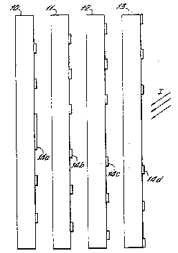
Referring now to Figure 2, this drawing illustrates
in cross-section the use of 4 adjacent panels 10, 11, 12
and 13 of electrical thickness ~/8 in a quarter wave zone
plate. In this and the rest of the drawings the paneis are
shown separated for clarity.
- On each of the panels 10, 11, 12 and 13 are
reflective portions 14a, 14b, 14c and 14d. These
reflective portions ~orrespond to the zones of a fresnel
zone plate and will be in the shape of rings on these
panels 10, 11, 12 and~13, excapt ~or the central zone of
zones 14a which will be disc shaped. The reflective
portions 14a, l~b, 14c and ~14d are on a ~ront ~ace facing
the incident signal I of each of the panels 10, 11, 12 and
13. The panels 10, 11, 12 and 13 can be made ~rom a
plastics material and to-simplify the construction o~ a
complete~zone plate, the p~rmittivity of the plastics can
be chosen such that the electrical-thickness of the panels
10, 11, 12 and 13 can be ~/8 where ~ is the wavelength
of the energy to be focused. Thus the panels can be put in
direct contact with~each other. `
WO92/Ot319 2 ~ PCT/GB9l/0ll36
-- 5 --
The reflective por~ions 14a, 14b, 14c and l~d can be
formed on the panels 10, 11, 12 and 13 by silk screen
printing, by using sal~ adhesive metal ~oil or by metalised
foil.
Figure 3 illustrates another embodiment of the
present invention wherein the reflective portions 14a, 14b,
14c and 14d are on a back face of each of the panels 10,
11, 12 and 13. This arrangement protects the fragilP
reflective portions 14d on panel 13 from accidental damage
at the surface of the zone plate.
Another arrangement is shown in Figure 4' wherein
only two panels 15 and 16 are used. In this arrangement
the reflective portions 14a, 14b, 14c and 14d are provided
on both front and back faces of the panels 15 and 16. The
spacing D between the panels can then be air or:a further
panel (not shown) having an electrical thickness of ~/8.
Using this arrangement it is possible to achieve
some variation in Dlectrical performance of the zone plate
structure.
Figure 5 illustrates a further example which
combines the features of Figures 2 and 4. In this example
~three panels 17, 18 and 19 are provided with panel 17 being
`provided with reflective portions 14a and 14b on a front
and back face and panels 18 and 19 being provided with
reflective portions 14c and 14d respectively.
, In Fi~ure 6 the re~lective portions 20, 21, 22 and
23 are provided on the front faces of the panels 10, 11, 12
and 13 as in Figure 2., However, the reflective portions
20, 21, 22 and 23 cover all of the face of each,respective
panel except for areas which are required to be transparent
to allow ~quartér wave ,phase correction. Thus the,,rear
~panel 10 need not have~ any transparent portions since no
signal will reach the areas not contribu~ing to ~/4 phase
; correction. This enables easier ¢ons~ruction since
: : : :
.:
.:
:
WO92/01319 2 Og 7 ~12 PCT/GB91/01136
." ''~.
- 6 -
this panel 20 can be totally reflective.
In Figure 7, ~ similar zone plate to that shown in
Figure 6 is illustrated, except reversed from the incident
radiaton. In this example, three panels 2~, 25, 26 are
provided to separate the reflective portions 20, 21, 22, 23
by ~/8. The front panel 27 need not be of any
particularly thickness but must provide support as a
substrate for the reflective portions 23. This panel 27
also serves the purpose of protecting the reflective
portions 23 from damage. The rear panel 28 is provided :'
purely for protection of the rear reflective portion 28. ;
In a further embodiment of the present invention,
the reflective portions of the zone plate are provided on 4 ~ ;
sheets of plastic film 34, as shown in Figures 8 and 9. In
this embodiment the sheets are separated by an e~ectrical
thickness of ~/8 using spacer panels 29, 30, 31. Two
outer panels 32 and 33 are also provided to protect the
,
sheets. In constructing such a zone plate the sheets 3
are formied by forming the respective zones or reflective
portions on the sheet and placing these sheets between
panels 29-33 so that they are correctly spaced.
Figures lO and ll illustrate-a simplification of the
construction of this type. In this example the sheets are
~ormed as one length.~ ~he sin~le sheet is then wrapped
around alternate panels 29, 30, 31. This simplifies the
assembly procedure o~ this type of zone plate.
In the arrangements illustrated in Figure5 2 and 3
where the re~lective portion correspondiny to zones of the
zone plake are ~ormed on ~only one face o~ the sheets, a
simple method of manufacture can be used. This -is
particularly the~ case~where, as in -the arrangements: of
Figures 2-and 3,~-~the- total surface area of the reflective
~portions ~~adds:up to the ;total surface area of the zone
plate. In such an~ arrangement all the reflective portions
for~the~zone plate can b~e;~cut out`of a single sheet of
~ .
- W~92/01319 ~ ~ 7 ~ ~ 2 PCT/~B9tlO1136 ! '
-- 7
,,
metalised film. The mth sheet (where m is the sheet
number which in these examples is between 1 and 4) has
applied to it the 1 + (4 (n ~ m - 2))th zone. More
generally for cases other than a quarter wave reflection
zone plate every mth sheet will have the 1 + (p tn + m -
2))th zone applied thereto, where p is the total number
of sheets. Thus the present invention is applicable to any
reflective zone plate and is not restricted to a quarter
wave zone plate.
A method and apparatus for manufacturing reflective
zone plates will now be described.
Figure 12 illustrates apparatus for the manufacture
of a reflection zone plate of the type illustrated in
Figures 2 and 3. A roll 40 of metalised film is provided
to be fed between a kiss-cutting punch and applicator 41
and a press base 42 to nip roller feeds 43.~ Reflective
portions corresponding to zones of a zone plate can then be
cut from the metalised film 51 by the action of the
kiss-cutting punch and application 41 on;the press base
4~2~ Waste metalised film is fed into: a waste catchment~bin
44, whilst the reflective portions~ are retained in the
applicator 41. A stack 45 of sheets of low loss dielectric
material is provided~and a single sheet 48 at a time is fed
through nip roller feeds 43 to a position between the
kiss-cutting punch and applicator 41 and press base 42.
During feeding tha sur~ace of sheet . 48 is subject to
anti-static treatment via a tinsel hrush 46: and is also
. ... .
coated With a suitable adhesive 47.i Once the~sheet 48 is ~ ~ -
in ~ position:~-under-~the ~applicator 41 -the~ appropriate
ellipses or reflective~portions~ corresponding to zones of a
~zone~platerare deposited and ~the sheet -48 is~-then fed out ~ ; ;
to form a stack-49.- Once the~correct number-of~shee~s~to; i`~ -
form~a ~ zone plate ~ar~ stacked~llght;~co~pression ;i3 ~applied
.
.
: , . . ~ :
W092/0l~l~ 2 ~ ~ 7 O 12 PCT/GB91/Ot136-
., --~ , . . .
- 8 -
' i'
to the stack 49 to adhere the sheets 48: the adhesive on
the surface not covered by the reflective portions
providing the adhesion~ Thus a laminate is formed ~hich is
- ready for fitting into an antenna assembly.
Figures 13a and 13b illustrate the structure of the
kiss-cutting punch and applicator 41. Elliptical blades 52
are provided protruding from the underside of the
kiss-cutting punch and applicator 41 to co-operate with the
press base 42 to cut the metalised film 51 to form the
reflective portions. The kiss-cutting punch and applicator
41 is urged towards the press base 42 to cut the metalised
film 51. When the cutting action is complete a vacuum is
applied through a porous sheet 50 provided on the lower
face of the kiss-cutting punch and applicator 41 to hol~
the reflective portions in place. The kiss-cutting punch
and applicator 4i is then raised and a sheet 48 of low loss
dielectric material transported to a position beneath it.
The kiss-cutting punch and applicator 41 is then lowered to
a position very close but not touching and a sIight
positive pressure is applied through~the porous sheet 50 to
the appropriate elliptical reflective portions to urge thqm
into posltion on the face of the sheet 48 of low loss
dielectrlc material, where they will adhere by the action
of the adhesive 47 applied during transportation of the
sheet 48.
The arrangement thus provides ~or accura~e alignment
of the respective zones of khe zone plate on the respective
sheets since the zones are cut from a single sheet of
metalised film and are deposited on the sheets at a single
-location. ~
- Thus- the ~xamples of the invention described herein-
above illustrate ~the simple construction of a phase
; correcting zone plate made ~ according to the present
invention. `~
., - ~ :. ~,-