Note : Les descriptions sont présentées dans la langue officielle dans laquelle elles ont été soumises.
CA 02087108 1998-03-31
._
NASTER PLATE OF OPTICAL MEMORY DEVICE
AND MANUFACTURING METHOD THEREOF
The present invention relates to a master plate of
an optical memory device for manufacturing the optical
memory device to or from which recording and reproducing of
information are optically carried out, and also relates to
a manufacturing method of the master plate of the optical
memory device.
The focus has been on an optical memory device
since that type of memory device has high density and large
capacity. The reason why the optical memory device has the
high density and large capacity is that a bit, which is a
recording unit for information, is restricted only to a
light beam diameter and thus the light beam can be set to
have a shape of about 1 micron.
However, this restricts the optical memory device
in many ways. More specifically, the light beam should be
positioned on the optical memory device with high accuracy
in order to record information on a predetermined recording
area and in order to reproduce recorded information from a
predetermined recording area. In general, an optical memory
device which is exclusively used for reproducing of
information can be arranged such that address information is
in advance contained in a recorded bit. Therefore, it is
possible to position the light beam for reproducing of
recorded information. But, it is impossible to carry out
recording of information on a write once-type memory or a
rewriteable memory so as to contain the address information
therein during the recording of information.
Accordingly, the write once-type memory or
rewriteable memory employ some guiding signal and guiding
address being in advance contained in a memory substrate of
the write once-type memory or rewriteable memory. For
example, the following is a general procedure: the memory
substrate of the write once-type memory or rewriteable
CA 02087108 1998-03-31
, .,._
memory are provided with grooves of physical protrusions and
recessions; and recording and reproducing of information are
carried out along the grooves. The grooves of the physical
protrusions and recessions are discrete in a circumferential
direction of the respective memories, thereby presenting pit
information indicative of each groove's address.
When the substrate of the optical memory device is
made of polycarbonate, an injection molding process using a
stamper having a pattern such as guiding grooves is widely
employed. The following deals with a conventional method
for manufacturing the stamper, with reference to Figure 3.
First, a master plate 11 having a pattern such as
guiding grooves is prepared (see Figure 3(a)). The master
plate 11 is coated with an electrode member 14 such as Ni,
the electrode member 14 being a thin film having a thickness
of the range between 20 nm and 100 nm (see Figure 3(b)). A
Ni electrocasted thin film 15, having a thickness of the
range between 200 ~m and 400 ~m is formed on the electrode
member 14 (see Figure 3(c)) by the electrocasting. Then,
the Ni electrocasted thin film 15 is removed from the master
plate 11. Thereafter, the other side of the Ni
electrocasted thin film 15 is polished (see Figure 3(d)),
thereby finishing the manufacturing of the stamper. As
mentioned above, the pattern such as the guiding grooves of
the master plate 11 i~ exactly copied to the stamper so as
to reversely form a pattern matching the guiding grooves on
the stamper. A good master plate 11 should be manufactured
in order to obtain a good stamper.
The following two methods for manufacturing the
master plate 11 are widely known: (1) a method for forming
a protrusion-and-recession pattern 52 on a glass substrate
51 by the use of photo resist (see Figure 4(a)); and (2) a
method for directly forming grooves of a protrusion-and-
recession pattern on a glass substrate 51 according to the
following steps: (a) making a mask by forming a pattern by
photo resist on the glass substrate 51, (b) carrying out dry
CA 02087108 1998-03-31
etc-hing to the glass substrate 51, and thereafter, (c)
removing the photo resist (see Figure 4(b)).
When the master plate manufactured according to
the method of Figure 4 (a) is observed by the STM (Sc~n~; ~g
Tunnel Microscope), it is confirmed that there exist a
plurality of minute physical protrusions and recessions on
the surface of the protrusion-and-recession pattern 52 of
the photo resist. In contrast, when the master plate
manufactured according to the method of Figure 4(b) is
observed by the STM, it is confirmed that a smooth pattern
such as the guiding grooves is formed by removing the photo
resist on which there exist residual minute physical
protrusions and recessions after the dry etching.
Accordingly, the master plate made by the etching is more
preferable than that by the photo resist in order to
decrease the noise.
The following conventional methods (1) to (3) are
well known as the method for directly forming the guiding
grooves and the like on the glass substrate. The following
deals with the conventional methods (1) to (3) with
reference to Figures 5 through 7.
According to the conventional method (1), guiding
groove patterns 22 are formed on a glass substrate 21 by the
photoresist (see Figure 5(a)). After the photo resist, the
dry etching is carried out by the use of a gas such as CF4,
CHF3 (see Figure 5(b)). After the dry etching, the residual
photo resist is removed (see Figure 5(c)), thereby directly
forming physical protrusions and recessions on the glass
substrate 21.
According to the conventional method (2), guiding
groove patterns 32 are formed on a glass substrate 31 by the
photo resist (see Figure 6(a)). The guiding groove patterns
32 are baked at a temperature above the softening point of
the photo resist (see Figure 6(b)). Thereafter, the dry
etching is carried out by the use of a gas such as CF4, CHF3
(see Figure 6(c)). After the dry etching, the residual
CA 02087108 1998-03-31
',_
photo resist is removed (see Figure 6(d)), thereby directly
forming physical protrusions and recessions on the glass
substrate 31.
According to the conventional method (3), guiding
groove patterns 42 are formed on a glass substrate 41 by the
photo resist (see Figure 7(a)). The dry etc-hing is carried
out with respect to the guiding groove patterns 42 by the
use of a gas such as CF4, CHF3 with ~2 gas (see Figure 7(b)).
After the dry etching, the residual photo resist is removed
(see Figure 7(c)), thereby directly forming physical
protrusions and recessions on the glass substrate 41.
In order to copy the shape of the guiding grooves
of the stamper to the polycarbonate substrate according to
the injection molding process, it is required that the mold
release of the polycarbonate substrate from the stamper is
carried out while the shape of the guiding grooves of the
stamper is kept unchanged, the polycarbonate substrate being
formed by carrying out the injection molding with respect to
the stamper.
However, according to the conventional method (1),
each edge portion of the guiding grooves rises upward
substantially perpendicularly. Therefore, the polycarbonate
substrate is likely to be caught by the edge portion of the
guiding groove when the mold release of the polycarbonate
substrate from the stamper is carried out, thereby making it
impossible for the polycarbonate substrate to keep the shape
of the guiding groove unchanged.
The object of the conventional methods (2) and (3)
is to improve the reliability, endurability and other
functions of the optical disk memory substrate by keeping
the respective continuity of a recording medium, a
protecting layer, and other materials which are formed on
the guiding grooves. The conventional methods (2) and (3)
attempt to achieve such continuity by inclining each edge
portion of the stamper so as to keep the continuity of the
formed thin film. However, the conventional methods (2) and
4~q:
CA 02087108 1998-03-31
'.,_.
(3) do not ensure that each edge portion of the stamper is
sufficiently inclined so as to avoid being caught by the
polycarbonate substrate during the mold release of the
polycarbonate substrate from the stamper.
More specifically, as shown in Figure 8, it is
assumed that the injection molding is carried out by the use
of the stamper which is obtained by the etched master plate
according to the conventional methods (1) to (3), the
stamper being composed of the electrode member 14 and the Ni
electrocasted thin film 15. When the mold release of a
polycarbonate substrate 16 from the stamper is carried out
in a direction of the arrow of Figure 8, each edge portion
of the guiding grooves is caught by the polycarbonate
substrate 16. Accordingly, the guiding groove pattern on
the polycarbonate substrate 16 is deformed (see the
reference numerals 16a and 16b of Figure 8), thereby arising
a problem, i.e., the deformed grooves are not appropriate
for leading a light beam which is converged onto the
substrate.
It is an object of the present invention to
provide a master plate of an optical memory device that can
form a stamper by which a substrate of the optical memory
device is obtained with repeatability.
In order to achieve the foregoing object, a master
plate of an optical memory device in accordance with the
present invention is characterized by comprising:
a substrate member having a plurality of guiding
grooves on a surface thereof, the guiding grooves being
spaced at a predetermined interval, each guiding groove
having edge portions:
wherein the edge portions are inclined with
respect to the surface of the substrate member, and inclined
angles of said edge portions with respect to the surface of
the substrate member are not more than 30~.
With this arrangement, the master plate of the
optical memory device is arranged such that the respective
~;
CA 02087108 1998-03-31
,. _
edge portions of the guiding grooves are inclined with
respect to the surface of the substrate member, and inclined
angles of the edge portions with respect to the surface of
the substrate are not more than 30~. Accordingly, even when
the copying is carried out with respect to the substrate of
the optical memory device according to the injection molding
process, wherein the stamper used is manufactured based on
the above-mentioned master plate, the mold release of the
stamper can be carried out without being caught by the
substrate. Thus, it is possible to keep the respective
~hApec of the guiding grooves of the stamper, thereby
enabling manufacturing of the substrate of the optical
memory device with high repeatability.
It is another object of the present invention to
provide a manufacturing method suitable for a master plate
of the optical memory device as above.
In order to achieve the foregoing object, the
manufacturing method of the master plate of the optical
memory device in accordance with the present invention is
characterized by comprising the steps of:
(a) coating a substrate member with a photo
resist thin film;
(b) exposing guiding groove patterns of the
master plate of the optical memory device by projecting
light onto the photo resist thin film;
(c) developing the resist thin film having the
exposed guiding groove patterns;
(d) post-baking the developed resist thin film at
a temperature which causes the resist thin film to be
deformed;
(e) carrying out dry etching after the post-
baking by use of a mixed gas including a first etching gas
for the substrate and a second etching gas for the resist
thin film; and,
(f) removing the resist thin film after the dry
etching process.
CA 02087108 1998-03-31
1!1_
According to the manufacturing method, by baking
the resist thin film at the temperature of more than the
deforming temperature of the photo resist during the post-
baking process, side portions of the resist thin film are
inclined with respect to the surface of the substrate
member. Further, by simultaneously carrying out etching of
the resist thin film having the above-mentioned shape in the
forming process of the guiding grooves on the substrate
during the etching process, the master plate of the optical
memory device can be manufactured wherein the guiding
grooves are formed such that each edge portion is greatly
inclined with respect to the substrate member and at an
angle of not more than 30~. Accordingly, even when the
copying is carried out with respect to the substrate of the
optical memory device according to the injection molding
process, wherein the stamper used is manufactured based on
the above-mentioned master plate, the mold release of the
stamper can be carried out without being caught by the
substrate. Thus, it is possible to keep the respective
shapes of the guiding grooves of the stamper, thereby
enabling manufacturing of the substrate of the optical
memory device with high repeatability.
Further scope of applicability of the present
invention will become apparent from the detailed description
given hereinafter. However, it should be understood that
the detailed description and specific examples, while
indicating preferred embodiments of the invention, are given
by way of illustration only, since various changes and
modifications within the spirit and scope of the invention
will become apparent to those skilled in the art from this
detailed description.
The present invention will become more fully
understood from the detailed description given hereinbelow
and the accompanying drawings which are given by way of
illustration only, and thus, are not limitative of the
present invention:
..,~
CA 02087108 1998-03-31
Figure 1 is an explanatory diagram showing the
main steps in a manufacturing method of a master plate of an
optical memory device in accordance with the present
invention;
5Figure 2 is an explanatory diagram showing the
condition where the copying is carried out with respect to
a polycarbonate substrate according to the injection molding
process, wherein the stamper used is manufactured based on
the above-mentioned master plate, and thereafter the mold
release of the polycarbonate substrate is carried out;
Figure 3 is an explanatory diagram showing the
step wherein the stamper is produced from the etched master
plate according to the conventional manufacturing method;
Figure 4 is an explanatory diagram showing the
difference between a conventional etched master plate and a
conventional photo resisted master plate;
Figure 5 is an explanatory diagram showing one
example of the conventional manufacturing methods of the
optical memory device:
20Figure 6 is an explanatory diagram showing another
example of the conventional manufacturing methods of the
optical memory device;
Figure 7 is an explanatory diagram showing still
another example of the conventional manufacturing methods of
the optical memory device; and,
Figure 8 is an explanatory diagram showing the
condition where the copying is carried out with respect to
a polycarbonate substrate according to the injection molding
process, wherein the stamper used is manufactured based on
the conventional master plate, and thereafter the mold
release of the polycarbonate substrate is carried out.
The following description deals with one preferred
embodiment of the present invention with reference to
Figures 1 and 2.
35The following deals with a manufacturing method of
the optical memory device in accordance with the present
~. ~
CA 02087108 1998-03-31
'~" .,~
embodiment, with reference to Figure 1. More specifically,
a substrate 1 is first coated with a photo resist having a
thickness in the range between 200 nm and 400 nm. The photo
resist is of a positive type such as AZ-1400 (trade name)
which is produced by "SHIPLEY CO. INC.". The coating is
made according to a method such as the spin coating method.
The substrate 1 is made of glass or quartz. After the
formation of the photo resist thin film, the photo resist
thin film is exposed, by the laser cutting method or the
contact printing method, so as to have patterns such as
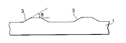
guiding grooves, and thereafter is developed. Figure l(a)
shows photo resist patterns 2 to which the development has
been made. The developed photo resist pattern 2, as shown
in Figure l(a), are defined such that respective edge
portions 3 of the photo resist patterns 2 rise upward
substantially perpendicularly with respect to the surface of
the substrate 1.
In that case, the photo resist patterns 2 are
disposed spirally or concentrically such that the pitch
between the photo resist patterns 2 is 1.6 ~m. In the case
where information is recorded on respective bottom portions
of the guiding grooves, the respective photo resist patterns
2 are formed such that the width of each pattern is
substantially 0.6 ~m. On the other hand, in a case where
information is recorded on respective land portions of the
guiding grooves, the respective photo resist patterns 2 are
formed such that the width of each pattern is substantially
1.0 ~m.
Next, post-baking is carried out with respect to
the developed photo resist patterns 2 at about 150~ C for 30
minutes. In that case, the post-baked photo resist patterns
2 become so softened as to be fluidized. Thus, the post-
baked photo resist patterns 2 change their shapes like
Figure l(b) due to the surface tension exerted on the
substrate 1. Note that the temperature of the post-baking
CA 02087108 1998-03-31
,_
is preferably a temperature of not less than that at which
the photo resist patterns soften.
Then, the reactive ion etching (hereinbelow
referred to as dry etching) is carried out for five minutes
under the conditions where the etching gas pressure of 10
mTorr is introduced and the high frequency output power of
400 Watt is applied. Note that CF4 gas is used during the
dry etching process as the etc-hing gas to be introduced, and
this CF4 gas contains a predetermined amount of ~2 gas.
According to the present embodiment, the flow rate of CF4 gas
is about 10 (SCCM) and the flow rate of ~2 gas falls in the
range between 4 (SCCM) and 10 (SCCM). Figure l(c) shows the
condition after the dry etching process. Respective edge
portions of the guiding grooves are greatly inclined with
respect to the surfaced of the substrate 1 according to
Figure l(c). Note that the depths of the guiding grooves
fall in the range between 50 nm and 80 nm. Note also that
CHF3 gas is preferably used as the etching gas.
More specifically, each edge portion 3 is greatly
inclined with respect to the surface of the substrate 1
based on the fact that (1) before the dry etching process is
carried out (see Figure l(b)), the photo resist patterns 2
have already been inclined with respect to the surface of
the substrate 1 due to the softening of the photo resist
patterns 2, and (2) isotropic etching is carried out with
respect to the photo resist patterns 2 because a
predetermined amount of ~2 gas is mixed during the dry
etching process.
At the final step, the residual photo resist is
removed. Thus, as shown in Figure l(d), an etching master
plate is obtained wherein inclined angle ~ of the edge
portions 3 with respect to the surface of the substrate 1
falls in the range between 23~ and 27~. The inclined angel
~ is hereinbelow referred to as an edge angle ~.
A stamper of Figure 2 is provided according to the
etched master plate manufactured by the above-mentioned
CA 02087108 1998-03-31
manner. The stamper is manufactured according to the
following steps. More specifically, the etched master plate
is first prepared and is coated with an electrode member 4
such as Ni, the electrode member 4 being a thin film having
a thickness of the range between 20 nm to 100 nm. A Ni
electrocasted thin film 5, having a thickness of the range
between 200 ~m and 400 ~m, is formed on the electrode member
4. The Ni electrocasted thin film 5 is removed from the
master plate and the other surface of the Ni electrocasted
thin film 5 is polished, thereby manufacturing the stamper.
The following deals with the comparison between
the edge angle of the stamper in accordance with the present
embodiment and that in accordance with the earlier mentioned
conventional methods (1) to (3), with reference to Table 1.
As is clear from Table 1, the respective stampers
which are manufactured by the master plates based on the
conventional methods (1) through (3) have their great edge
angles ~, i.e., 49~ to 83~. Accordingly, the edge portions
of the polycarbonate substrate are caught by the injection-
molded polycarbonate substrate when the mold release of the
stamper from the injection-molded polycarbonate substrate is
carried out, thereby deforming the corresponding portions of
the polycarbonate substrate.
Note that according to the conventional methods of
Table 1, edge angle ~ is greater in the case where ~2 gas is
not mixed than in the case where ~2 gas is mixed during the
dry etching process. Further, as is clear from Table 1,
even when the master plates are made based on the same
conventional method (3), the higher the amount of ~2 gas that
is mixed, the smaller are the respective edge angles H of
the provided stampers.
According to the comparative example of Table 1,
the flow rate of ~2 gas is set to be 2 (SCCM), but the
temperature of the post-baking and the flow rate of CF4 gas
are the same as those of the present embodiment. In the
comparative example, the edge angle ~ is 42~. Therefore,
CA 02087108 1998-03-31
~. _
the edge portions of the polycarbonate substrate are caught
by the stamper when the mold release of the injection-molded
polycarbonate substrate from the stamper is carried out,
thereby deforming the corresponding portions of the
polycarbonate substrate (see reference numerals 16a and 16b
of Figure 8).
In contrast, the stampers manufactured by the
master plate based on the method of the present embodiment
have an edge angle ~ which is less than 30~, i.e., 23~ to
27~, the stampers being manufactured under conditions where
the temperature of the post-baking process is set to be
about 150~ C and the flow rate of ~2 gas is set to be at
least 4 (SCCM). Accordingly, no edge portion of the
polycarbonate sub~trate 6 is caught (see Figure 2) by the
stamper when the mold release of the injection-molded
polycarbonate substrate from the stamper, which is composed
of the electrode member 4 and the Ni electrocasted thin film
5, is carried out in the direction of the arrow of Figure 2.
Thus, the respective shapes of the guiding grooves of the
stamper can be kept unchanged, thereby enabling the
substrates for use in the optical memory device to be
obtained with repeatability.
As mentioned above, according to Table 1, the
required flow rate of ~2 gas to be mixed during the dry
etching process is at least 4 (SCCM) and the required
temperature of the post-baking process is about 150~ C. The
resisted thin film softens so as to be fluidized since the
temperature of the post-baking process is set to be 150~ C,
thereby making the side portions of the post-baked resist
thin film inclined with respect to the substrate surface.
In the process of the formation of the guiding grooves on
the substrated surface during the dry etching process, the
etching of the resist thin film having a shape as above is
simultaneously carried out, thereby making the respective
edge portions of the guiding grooves greatly inclined with
respect to the substrate surface. Thus, the master plate of
,
CA 02087108 1998-03-31
the optical memory device having the inclined angle of not
more than 30~ can be manufactured.
The master plate of the optical memory device in
accordance with the present invention, as mentioned above,
is arranged such that the respective edge portions of the
guiding grooves are greatly inclined with respect to the
substrate surface, and the inclined angles with respect to
the substrate surface can fall within 30~.
Therefore, even when copying is carried out with
respect to the substrate of the optical memory device
according to an injection molding process, wherein the
stamper used is manufactured based on the master plate of
the optical memory device in accordance with the present
invention, the mold release of the stamper can be carried
out without being caught by the substrate. Thus, it is
possible to keep the respective shapes of the guiding
grooves of the stamper, thereby enabling manufacturing of
the substrate of the optical memory device with high
repeatability.
The manufacturing method of the master plate of
the optical memory comprises the following steps: (1)
coating a substrate with photo resist thin film; (2)
exposing guiding groove patterns of the master plate of the
optical memory device by projecting light onto the photo
resist thin film; (3) developing the resist thin film having
the exposed guiding groove patterns; (4) post-baking the
developed resist thin film at the temperature which causes
the resist thin film to be deformed; (5) carrying out dry
etching after the post-baking by the use of mixed gas,
including an etching gas for the substrate and an etching
gas for the resist thin film; and (6) removing the resist
thin film after the dry etching process.
Therefore, the side portions of the resist thin
film are inclined due to the deformation thereof during the
post-baking process. The respective edge portions of the
guiding grooves are greatly inclined with respect to the
CA 02087108 1998-03-31
substrate surface during the dry etching process since the
isotropic etching is carried out with respect to the photo
resist thin film having the above-mentioned shape.
Accordingly, the master plate of the optical memory device
having the inclined angle not more than 30~ can be
manufactured.
Moreover, even when the copying is carried out
with respect to the substrate of the optical memory device
according to the injection molding process, wherein the
stamper used is manufactured based on the master plate of
the optical memory device in accordance with the present
invention, the mold release of the stamper can be carried
out without being caught by the substrate. Thus, it is
possible to keep the respective shapes of the guiding
grooves of the stamper, thereby enabling manufacturing of
the substrate of the optical memory device with high
repeatability.
There are described above novel features which the
skilled man will appreciate given rise to advantages. These
are each independent aspects of the invention to be covered
by the present application, irrespective of whether or not
they are included within the scope of the following claims.
CA 02087108 1998-03-31
'"",_
Table 1
POST-BAKE CF4 FLOW ~2 FLOW EMPLOYED ~ EDGE IS
TEMP.(C~) (SCCM) (SCCM) METHOD (~) CAUGHT?
0 METHOD (1) 83 YES
2 METHOD (3) 74 YES
4 METHOD (3) 70 YES
6 METHOD (3) 67 YES
8 METHOD (3) 64 YES
METHOD (3) 62 YES
0 METHOD (2) 49 YES
COMPARATIVEA LITTLE
2 EXAMPLE 42 BIT
PRESENT
4 EMBODIMENT 27 NO
150 PRESENT
6 EMBODIMENT 26 NO
PRESENT
8 EMBODIMENT 24 NO
PRESENT
EMBODIMENT 23 NO
Note that methods (1) to (3) of Table 1 correspond
to conventional methods respectively and ~ indicates an edge
angle.
,~