Note : Les descriptions sont présentées dans la langue officielle dans laquelle elles ont été soumises.
W092/03019 l ~ 0 7 PCI/CAgo/00244
-
METHOD AND APPARATUS FO~ IMAGE DATA PROCE~ING
B~CRGROUND
The present invention relates to a method and appara~u~
for processing image data for transmission along telephone lines
and for decoding the processed data after transmis~ion such that
the data can be transformed to produce colour images of colour
television quality.
Known systems for transmitting image data along
telephone lines are severely limited in the speed at which the
data can be transmitted and reassembled at a receiving end. For
example, a single frame of a colour television quality image
contains 512 by 512 by 24 bits and takes approximately 90 seconds
to transmit without compxession using a 64 kilobit per second
st~nA~rd ISDN B channel. One method to enhance tr~n 1ssion
speed is to compress the data according to known transforms and
then, after transmission, to decompress the compressed,
transmitted data.
A television screen, for example, is divided up into
a plurality of individual image units referred to as pixels. For
colour images each pixel may contain three separate parameters
such as red, green and blue. Each parameter may be defined as
to intensity by an eight bit number called a byte. Thus, each
pixel is defined by three bytes. In order to process the data
efficiently it is useful to treat a block of 8 by 8 pixels known
as a "tile". A known technique consists of directing a first
tile of an image into a processor and then inputting the first
tile into a digital transformer. The tile output modified by the
transformer is sent back to the processor where it is further
compressed and sent to an output port. The second tile in the
image is then sent to ~he transformer. This process is repeated
until all of the image tile have been processed. In such a
system the requirement for numerous fetch and other instructions
from the processor makes the process impractically slow. Thus,
the advantages of transmission speed increase due to compression
WO92/03019 2~8~ 2 PCr/CAgo/
is offset by the time take to compress and decompress.
.
Accordingly, it is an ob-Ject o~ the invention to
provide an improved method o~ processil1g imag~ng data ~or
compression and decompression. It is a further ob~ect o~ the
invention to provide a buffer to receive and ~tore da~a
corresponding to an image an~ then to process the captured data.
8UMMARY OF T~E lN V~ lON
According to the invention there is provided a method
of processing digital image data such as obtained from a
television screen for transmission along telephone lines in a way
that the transmitted data can be transformed to produce images
in colour. The method includes storing a frame of digital data
in a frame buffer, transferring a group of tiles from said frame
buffer to a tile buffer, generating a clock signal, and
generating address and sets of control signals in a state
machine. The clock signal is applied to a digital transformer
while the address and set of control signals are applied to the
tile buffer to directly transfer a block of data in the tile
buffer to the digital transformer. After the data is transformed
in the digital transformer it is returned to the tile buffer
where it is used to overwrite the corresponding original block
of data stored in the tile buffer. The latter process is
followed by coding the transformed tiles stored in the tile block
so as to compress them The process is repeated until all tiles
in the frame buffer have been compressed.
Preferably the group of tiles is transferred directly
to the tile buffer. The clock signal may have a frequency of
greater than approximately one megahertz. Advantageously, the
digital transforming step applies a discrete cosine transform
while the coding is Huffman coding.
An imp~ GV - ?nt in speed is achieved by utilizing Y, I
.
WO92/03019 3 ~ Q8,~ ~ 0 7
and Q parameters to define a pixel c ur. By alternating I and
Q data in each alternate pixel, a ~aving o~ l/3 o~ the data
required to describe the image is achieved without a ~igni~lcant
loss of resolution or colour.
The compressing step may inalude sequentially
transferring tiles of the data into a tile buf~e~ and per~orming
a discrete cosine transform on each o~ the tiles, The
transformed tiles are t~en coded in accordance with Hu~fman
Coding. The DCT and Huffman Coding are de~cribed in ISO/CCITT
JPEG-8-R5.2 standard recently published.
The tile pixels in the frame buffer are extracted row
by row tile by tile until an entire row of tiles has been
transferred. commencing from the first row and proceeding in
sequence row by row until the last row has been extracted.
The video signals, if in analog form are first
digitized before storing a frame of them in the frame buffer.
After compressing the data it is transferred to a communication
ouL~uL interface.
The method may also include reversing the order of
processing to perform first inverse Huffman Coding on compressed
data, followed by inverse Huffman Coding and then transferring
the decompressed data to the frame buffer for further transfer
to be transformed into analog video signals~.
BR~EF DE8CRIPTION OF T~E DRAWING~
The novel features believed characteristic of the
invention are set forth in the appended claims. The invention
itself, however, as well as other features and advantages
thereof, will be best understood by reference to the detailed
description which follow, read in conjunction with the
accompanying drawings, wherein-
W092/03019PCT/CA90/00~4
~08~507 - 4 ~ ~_
Figure 1 is a block diagram o~ a conventional ~yPtem
for processing image data;
Figure 2 is a block diagram of a pre~erred apparatu~
for processinq image data ~rom analog video source such a~ a
television monitor;
Figure 3(a) and 3(b) are schematic diagrams showing a
portion of a row of pixels in a part of the frame buffer to
demonstrate their composition for two different choices of
parameters to describe colour and intensity;
Figure 4 is a timing diagram showing the movement of
tiles into and out of the discrete cosine transform chip;
Figure 5 is a schematic block diagram showing the state
machine and its output of address and control signals which
govern the flow of data between the frame buffer, the tile buffer
and the discrete cosine transform;
Figure 6 is a table showing the structure of the
address bits generated by the state machine which are used to
transfer data between the frame buffer, the tile buffer and the
discrete cosine transform (DCT); and
Figure 7 is a block diagram showing a more detailed
system corresponding to that shown in Figures 2 and 5 hereof.
D~TAILED DE8CRIP~ION ~ITH REFERENCE TO THE DRAWING8
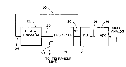
Referring to Figure 1 there is shown a conventional
system for processing image data received from a video source in
analog form on line 12. The signals on line 12 are converted to
digital signals by analog to digital converter 14, outputted on
line 16 to a ~rame buffer 17 and then to a processor 18. The
processor transmits the data on line 20 to a digital transformer
.~,
.. .
WO92/03019 PCT/CA90/00~
! ,, 22 which modifies the data and returns it back to the proce~or
18 ~here it is then sent along line 30 to a telephonQ line ~or
transmission. The digital transformer 22, which per~oxms a
discrete cosine transform on tile6 made up o~ a block o~ R plxel~
by 8 pixels, inputs and outputs its dat~ in a predePlnQd order.
This required ordering of the data is determined by the internal
structure of the digital transformer 22. The image data received
by the processor 18 from the frame buffer 17 are sent to and
received from the digital transformer 22 in tiles of 8 pixels by
8 pixels in the order expected by the digital transformer 22.
Each tile of image data from the frame buffer 17 is directed
through the digital transformer 22 and further processed by the
processor 18 in order to compress the image. Although data is
compressed by the transformer 22, the time for compression and
subsequent decompression on a receiving end (not shown) would
offset any advantage due to increased speed of transmission.
Referring to Figure 2 there is shown a system in
accordance with a preferred embodiment of the invention in which
analog signals on line 12 are converted to digital signals on
line 16 by an analog-to-digital converter 14. The digitized
image data from the analog to digital converter 14 is sent on
line 16 to a frame buffer 32 in which the image data is
temporarily stored or captured. The frame buffer 32 consists of
8 one megabit video dynamic random access memory chips (called
"VRAMSI') made by Texas Instruments Incorporated which form two
image memory units each of 512 X 512 X 16 bits capacity. Data
in the frame buffer 32 is stored in rows with each block of 8
pixel x 8 pixel ~orming a tile. A first row of tiles ("row O")
is moved into the tile buffer 37 from the frame buffer 32 along
line 35 in response to control signals from a state machine 58.
The memory 39 of the tile buffer 37 tsee Figure 7) consists of
enough high speed static random access memory (SRAM) chips 41 to
contain one row of 8 pixel by 8 pixel tiles from the frame buffer
32. The state machine 58 moves the first two tiles in the tile
buffer 37 into the digital transformer 36, which in this case is
a discrete cosine transform chip manufactured by INMOS in the
WO92/03019 2 0 ~ ~ r~ ~ 7 - 6 - PCT/CA90/002~
United Kingdom and sold under part number lMSA121 (herein~.ter
referred to as a "DCT"), wher~ they are proce~3ed and ~hen
transferred back to the tile buf~er 37. ~he ~tate machine 58
presents the individual pixel~
of each tile to the DCT chip 36 in the order requir~d by the DCT
chip 36. In addition, the state machine 58 overwrites each tile
in the tile buffer 37 with the resulting DCT coe~ficients
generated by the DCT chip 36. The DCT chip 36 takes 8 pixel x
8 pixel tiles, performs a discrete cosine transform, and then
outputs the results.
Following the transformation of the first two tiles
from the tile buffer 37 through the DCT chip 36, each remaining
pair of tiles in the tile buffer 37 is directed through the DCT
chip 36 by the state machine 58 until all of the tiles have been
transformed and their resulting DCT coefficients are stored back
in the tile buffer 37. The DCT coefficients in the tile buffer
37 are then accessed by a digital signal processor (DSP) 42 chip
which commences a coefficient to symbol conversion, namely such
as Huffman coding, on the data. Other types of conversion are
possible. The DSP chip 42 is manufactured by Texas In~LLI ?nts
Incorporated under part number TMS320C25. The resulting
compressed data from the DSP 42 is then sent to a communication
card 74 and is ultimately sent over a telephone line or stored
on a hard disk drive (not shown).
While the DSP chip 42 is performing coefficient to
symbol conversion, the state machine 58 begins operation on the
second row of tiles (row 1) in the frame buffer 32. It transfers
this row of image data to the tile buffer 37 and, once again,
runs this data through the DCT chip 36 and deposits the results
back in the tile buffer 37 for the DSP 42 to eventually access.
Row by row of tiles from the frame buffer 32 are transferred to
the tile buffer 37, transformed by the DCT 36, and then directed
to the DSP 42 for coefficient to symbol conversion until the
entire image, comprised of all 64 rows of tiles, has been
compressed. The data movement operations caused by the state
machine 58 and tha procecs;n~ by the DSP 42 may occur
concurrently so that discrete cosine transformations may occur
.
W092/03019 _ 7 ~ 0 7 PcT/cAIgo/oo~
in parallel with Huffman codiny, 'further increa~ing the
com~ression speed.
The circuit of Figure 2 can al~o receive compr~s~ed
data on line 44 into the DSP 42 which applies a ~ymbol to
coefficient conversion known afi reverse Hu~man coding. Other
types of conversion are also possible. Following operation by
the DSP 42, the data is transferred to the tile bu~fer 37 from
which it goes into the DCT 36. The DCT chip 36 is con~igured to
apply an inverse transform and hence decompress the data. The
decompressed data is written into the frame buffer 32 from which
it can be directed to a desired output.
Referring to Figure 7 there is shown a more detailed
diagram of the imaging system. Here analog video signals
received by a daughter card 66 are digitized and sent to shift
register 62 which is incorporated into the frame buffer 32
together with the ~RAM chip 64. The frame buffer 32 is
controlled by a video system controller chip 68 which refreshes
the frame buffer 32 and arbitrates access to the frame buffer 32.
The DSP 42 has its own discrete memory 43 consisting of 64
kilobytes of high speed static ram memory 41 and 32 Kilobytes of
electrically erasable programmable only memory (EPROM) 39.
Output from the DSP is through either a communication daughter
card 74 or to a host interface 70 couplable to a host computer
72.
Each pixel 46 of frame buffer 32 is shown schematically
in Figure 3(a) as consisting of three parameters such as red 47,
green 48 and blue 49. The intensity of each colour component is
described by an 8 bit number. Other means of describing the
colour and intensity o~ a pixel may be used. The method employed
in the present invention consists of choosing a parameter Y
corresponding to intensity and two parameters I and Q which
correspond to colour. It is possible with such a choice to
reduce the number of'bytes reguired in each pixel from three to
two by alternating I and Q in adjacent pixels as shown in Figure
WO92/03019 PCT/CA90/00~
3(b) without ~a8c~lng noticeably from th~ quality o~ the
picture. Thus, each tile con6ist~ o~ an ~ pixel x 8 pixel block
with each pixel having a number o~ bit~ to describe ite colour
and intensity.
Image data in the frame bu~er 32 i~ stored in a YIQ
format. With respect to figure 2, when a row o~ tiles i~
transferred from the frame buffer 32 to the memory of the tile
buffer 37, the Y, I and Q components are all transferred into the
tile buffer memory 41. However, the state machine 58 first sends
all of the Y image components of all tiles in the tile buffer 37
through the DCT chip 36, followed by the I then Q components.
once the operation of the DCT chip 36 is complete, the DSP 42 is
able to access the DCT coefficients in the tile buffer 37 for all
three components Y, I, and Q.
To appreciate the timing of transferring tiles Figure
4 shows that the first two tiles are transferred sequentially to
the DCT 36 and are returned to the tile buffer before the next
two tiles are extracted from the frame buffer 32 and placed in
the tile buffer 37. Thus, there is a delay of two tiles
introduced by the return of processed tiles from the DCT 36.
The operation of the state machine 58, implemented with
programmable array logic the chips for which are commonly
referred to as PAL's, is controlled by the digital signal
processor 42. Upon informing the state machine 58 of the
required operation, such as a frame buffer 32 to tile buffer 37
trans~er or DCT 36 transformation, by depositing a specific
con~ol value in a state machine control register 60 (see Figure
5), the DSP 42 sends a signal to the state machine 58 informing
it to "go". ~he state machine 58 performs the operation
requested by the DSP 42 and, upon completion, sends an "I'm done"
signal to the DSP 42. While the state machine 58 is performing
an operation the DSP 42 is free to do other tasks.
- When performin~ any transfer operation, as seen in
WO92/03019 _ 9 ~ rjo 7 PCr/cAgo/Oo~M
Figure 5, the state machine 58 must generate address ~gnals ~or
the tile buffer 37 and frame buffer 32 and ~ontrol ~iqnal~ ior
the tile buffer 37, frame buf~er 32, and DCT chip 36. The
address generated by the state machine 58 ori~lna~es ~rom a group
of counters 46 divided into addre~s ~ields. Each ~ield o~
addresses may be independently incremented by the state machine
58. The concatenated address fields form the ~ull address used
by both the tile buffer 37 and the frame buffer 32 memories.
Individual address fields may define the tile number "t", row
number "r", and column number "c" transferred at any given time
in a state machine operation. By examining a control register
60 of the state machine 58 and the current address of the address
fields, the state machine 58 is able to decide the appropriate
"next address" for the next data transfer and pulses the
appropriate increment signal on selected ones of lines 56 to the
counters 46 so that that address is generated. The control
signals inform the tile buffer 37, frame buffer 32, and DCT chip
36 when to read and write data. They are generated by the state
machine 58 by examining the state machi~e control register 60
and the current state of the state machine 58.
The state machine addresses, shown in detail in Figure
6, each consist of 13 bits divided up into four different fields.
The fields are write "w", row number "r", tile number "t" and
column number "c". Together r, t, and c produce an address which
points to a single pixel or coefficient within the frame buffer
32 or tile buffer 37. The tile field "t" indicates the current
tile which is involved in a state machine transfer. There are
64 Y tiles and 32 of each of the I and Q tiles contained within
a row of tiles. Therefore, 6 bits are required to indicate a
unique Y field of a tile and 5 bits to indicate a unique I or Q
field. The row ~ield "r" indicates the row, numbered from 0 to
7 and the column field indicates the column numbered from 0 to
7 within the given tile. The value in the single bit write field
is used to determine whether a tile buffer "read" or tile buffer
"write" will occur during transfers to and from the DCT 36.
Because I image components are stored only in even pixels in the
WO92/03019 c~o~ 5 0 7 - lo - PCI/CA90/002
frame buffer and Q image components are stored only in odd pix~l~
in the ~rame buffer, as shown in Figure 3(b), the arrangement
for the I and Q tile and column ~ield~ di~er ~rom the Y
component's tile and column ~ield arrangement.
The state machine carries out the Pollowing ~ive
different transfer operations:
(l) Transfer of a row of tiles from the frame bu~er
32 to the tile buffer 37.
(2) Trans~er of a row of tiles from the tile buffer
37 to the frame buffer 32.
(3) Transfer the Y component of the tiles in the tile
buffer through the DCT chip 36 and back into the tile buffer 37.
(4) Transfer of the I component of the tiles in the
tile buffer 37 tiles through the DCT chip 37 and back into the
tile buffer 37.
(5) Transfer of the Q component of the tiles in the
tile buffer 37 through the DCT chip 36 and back into the tile
buffer 37.
The address generated by the state machine 58 flows to
both the tile and frame buffers 37 and 32, respectively. As an
example, when setup by the DSP 42 to perform a frame buffer 32
to tile buffer 37 transfer and told to "go", the state machine's
address fields are initially all e~ual to zero. The address is
pointing, therefore, to row 0 and column O of tile 0, which is
the first pixel in both the frame and tile buffers 32 and 37,
respectively. A read signal is sent to the frame buffer 32, a
write signal is sent to the tile buffer 37 and the first word of
image components is transferred directly from frame buffer 32 to
the tile buffer 37.
W092/03019 ~ 8 ~ ~ ~ 7 PC~/CA90/00~
Immediately following the aforementioned pixel
transfer, the state machine 5~ examine~ the current state of the
address fields and the type t~ trans~er reque~ted. It uses this
information to determine the proper "next addre~s" required and
stro~es the appropriate increment pulses to generate that
address. In this case, increment pulse 0 would be strobed
resulting in the column field being increased to 1. The second
pixel is then transferred directly from the frame bu~er 32 to
the tile buffer 37 by the state machine 58 by again strobing the
appropriate read and write control signals.
The state machine 58 continually strobes the
appropriate increment pulses to generate the required address and
the read/write control signals to initiate the frame buffer 32
to tile buffer 37 transfer until all pixels in the selected row
of tiles in the frame buffer 32 have been transferred to the tile
buffer 37. The full address sent to both the frame buffer 32 and
tile buffer 37 is simply incremented by one for each pixel
transfer, in a frame buffer 32 to tile buffer 37 transfer, until
the state machine 58 detects that the last transfer ( the 409Sth
pixel) has been accomplished. At this time, the state machine
58 sends an "I'm done" signal to the DSP 42 to indicate the
completion of the requested operation.
When the state machine 58 is conditioned by the DSP 42
to transfer data to and from the DCT 36 and told to "go", for
each DCT chip 36 clock cycle, the state machine 58 must send an
expected pixel or coefficient of data to or cause the tile buffer
37 to receive it from the DCT chip 36. The DCT chip 36 requires
input and o~ data to be handled in a strict order. For
example, the DCT chip 36 requires data to be presented to it row
by row within a give tile. The state machine is able to generate
the proper address by examining the type of DCT operation in
p~Gy~eo8 ~Y, I, or Q) and the current state of the address field.
The address initially points to row and column 0 of tile 0. As
data is transferred from the tile buffer 37 to the DCT chip 36,
the column address field is first incremented until it reaches
WO92/03019 2 0 ~ ~ 5 ~ 7 - 12 - PCr/CA~O/OO~
a maximum, i.e. 7. For the next transfer the column addiL_~
field is reset and the row field is incremented. Eventually,
when both the column and row addres~ field reach their maximum
value, they are reset and the tile field is incremented. Us~ng
this technique to generate the addre~s flowing to the tile bu~er
37, the DCT chip 36, is able to receive tlle input data in the
appropriate order. Output data from the DCT chip 35, directed
to the tile buffer 37, is stored back in the appropriate tile,
column, and row address locations using the same address
generation technique. The write field indicates whether a tile
buffer to DCT chip or DCT chip 36 to tile buffer 37 data transfer
is currently occurring. Once all tiles within the tile buffer
37 have been directed through the DCT chip 36, the state machine
58 sends an "I'm done" signal to the DSP.
It is possible to use adaptive Huffman Coding rather
than Huffman Coding. However, in the latter case it would
require transferring back transformed data after operation of the
DCT into the frame buffer as adaptive Huffman Coding requires
that the whole of the intermediate results be looked at.
Accordingly, while this invention has been described
with reference to illustrative embodiments, this description is
not int~nded to be construed in a limiting sense. Various
modifications of the illustrative embodiments, as well as other
embodiments of the invention, will be apparent to persons skilled
in the art upon reference to this description. It is therefore
contemplated that the appended claims will cover any such
modifications or embodiments as fall within the true scope of the
invention.
.,
.
,