Note : Les descriptions sont présentées dans la langue officielle dans laquelle elles ont été soumises.
WO 92/06396 ~ PCT/US91 /07416
Integrated Optics Device Mounting rcr
Thermal arid uiah G-Shock Isolation
Technical Field
This inventi~.~. relates to mounting structures _~r
integrated optics devices, more particularly to such
structures allowing the optics device to operate ~r
severe thermal and G-shock load environments.
Background Art
L'.S. Patent x,-50,800 ('800) to Fournier et al.,
assigned tc the assignee cf the present ,invention,
articulately presents an explanation cf the backarcund
art involved in t~:e r.ounting of integrated cptics
devices to substrate ~,aterials. Although a good
approach, t his attempt had several shcrtco.;,ings.
1~ '800 teaches an apparatus comprising a lithium
niobate ( LiNbO., j integrated cp tics ( IO ) chip mounted ....
J
a LirdbO., substrate :. i th an ui traviole t cured adhesiva .
The substrate is mounted to a support package structvrs
with a compliant adhesive bonding. ::oweve= the
substrate must be at least ten times the thickness c~
the I0 chip in order to reduce the therma~y-~y~ and G-shoe::
induced stresses transmitted throucrh the substrate ~=cr,
the support package.
This constraint presents a problem since LiNbO..
with a 10 miliimeter(mm) thickness is not available as a
stock size and therefore is more expensive to procure.
In addition, if the thickness of the substrate is
reduced, less volume is required for the packaging along
with less weight for the system in which the IO chip
;0 operates.
WO 92/06396 PCT/L.'S91 /07416
One application for integrated optics chips __ i~:
fiber optic rotation sensors (e. g., a fiber cotic cyrc;
which may be used to provide guidance fcr precisic.~,
guided weapons and tactical missiles. In particular,
fiber optic rotation sensors may be employed in smart
artillery shells such as the proposed Advanced
"Copperhead". Since this type ef shell is launched fro:
an artillery piE.ce (e. g., a 155 millimeter howitzer;,
high G-shock loads occur when the shell is being fired.
_.. This type of launching places a great deal of shock cn
components within the shell and thus innovative
packaging techniques must be used if active electronics
are to be placed within the shell.
The active electronics envisioned operatincr withi.~.
__ these shells must sustain 20,000 G shock loads. This
requirement creates a tremendous problem to designers
involved with fiber optic rotation sensors since the
performance of the LiNbO., IO chip is susceptible ....
J
stresses transmitted through the substrate. These
_" stresses spuriously chance the refractive index .._ t:.e
IO chip, thereby interfering with the modulation beinJ
performed in the I0 chip as part cf the well known
signal processing in the rotation sensor. This
interference results in an error in the detected
rotation rate of the rotation sensor and hence reduced
sensor performance and accuracy.
Disclosure of Invention
An object of the present invention is to provide
reduced stress mounting for an IO chip which can sustai-:
~~ high G-shock loads.
According to the present invention, an integrated
optics chip comprising an optical signal path disposed
CA 02088578 2001-07-17
64159-1243
- 3 -
in a principal plane c>f a crystalline chip having a known chip
thickness, anisotropic thermal characteristics, and
crystallographic orientation, is mounted to a first surface of
a similar thermally a.ni;~otropic material substrate, and a
second surface of the substrate, spaced from the first surface
at a substrate thickr..ess approaching the known chip thickness,
is bonded to a mountiri.g surface with a pressure sensitive
acrylic film adhesive having a flexible highly energy
dissipative polymer having visco-elastic properties, whereby
1G using the pressure sensitive acrylic film adhesive allows a
substantial reduction from that in the prior art in the
thickness of the sub~;t:rate as compared to the thickness of the
IO chip.
Therefore this invention seeks to provide an
15 apparatus for. mountir~q an integrated optics device having an
optical sign~~l path fabricated in a crystalline chip of a
certain thicl~.ness and crystallographic orientation selected to
provide anisotropic thermal expansion in the principal plane of
the optical ;signal pat:.h and having certain anisotropic
20 coefficients of thermal expansion, comprising: a substrate
comprising crystalline material having a similar
crystallographic axe: orientation and similar aniostropic
coefficients of thermal expansion to those of the crystalline
chip, and having sub~~t~rat:e first and second mounting surfaces
25 spaced a substrate th~.ckness apart, said substrate first
mounting surface being adapted to receive the crystalline chip
in bonded relationshif:> thereto with mutual crystallographic
orientation of the chip principal plane with said substrate
first mounting surface; and package enclosure means having an
3() enclosure mounting surface, characterized by: said enclosure
mounting sur:Eace beinc:~ bonded to said substrate second mounting
surface with a visco--elastic polymer adhesive.
CA 02088578 2001-07-17
64159-1243
- 3a -
This invention also seeks to provide the method of
mounting, to a surface, an integrated optics (IO) device of the
type having a.n optical path disposed on a crystalline chip
having anisotropic thermal characteristics, comprising the
steps of: determining the coefficients of thermal expansion of
the chip and the orient<~tion of the chip crystallographic axes
in the principal plane o:f the optical signal path; providing a
crystalline material substrate having a similar
crystallographic axes orientation and similar anisotropic
coefficients of therrr~a.l expansion to those of the chip, and
having substrate first.<~nd second mounting surfaces spaced
apart at a substrate t.h:ickness; fastening the chip to said
substrate to provide mul~ual crystallographic orientation of the
principal plane with said substrate first mounting surface; and
1~ bonding said substrate second mounting surface to the surface
with a visco-elastic polymer adhesive.
These and ot:h~=r objects, features and advantages of
the present invention will become more apparent in light of the
following detailed description of a best mode embodiment
thereof as i7_lustratec~ in the accompanying drawing.
Brief Description of th~? Drawin
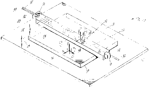
The sole FI:CiU:RE in this application is a perspective
illustration of an IC> chip low stress mounting structure in
accordance w=~th the pz:esent invention.
Best Mode for Carrying Out the Invention
The sole F7:CJURE which is not drawn to dimensional
scale, illustrates an IO chip low stress mounting structure 10
comprising an IO chip 12 bonded to a substrate 14. For
illustrative purpose~~ the IO chip consists of a simply "Y"
shaped optic<~l waveguide 16,
CA 02088578 2001-03-05
64159-1243
- 4 -
disposed in LiNb03 by means known in the art, e.g. ion exchange
or titanium diffusion. The LiNb03 IO chip has angled chip
endings 18, 20 of approximately ten degrees to reduce the
reflections, and a crystal surface 21 spaced at a crystal
thickness (t) 22 from a crystal mating surface 24 (i.e., IO
chip bottom surface which is not shown); both surfaces lying in
the principal plane of the IO chip. The mating surface 24 is
bonded along its entire surface to a mounting surface 28 of the
substrate 14.
The IO chip 12 is positioned on the mounting surface
28 and partially overhangs the substrate 14. Fiber carriers
30-32 are mounted to the angled chip endings 18, 20 to support
input and output optical fibers 36-38. The optical fibers may
be single mode fibers with a core diameter on the order of 4-12
microns and a cladding diameter of approximately 70-130
microns. U.S. Patent 4,871,226 to Courtney et al. and assigned
to the assignee of the present invention discloses the mounting
of the fiber carriers to the angled chip endings.
The LiNb03 IO chip thickness (t) 22 is approximately
1.0 millimeter, with length and width selected by the
particular application. The IO chip is an X-cut crystal, i.e.,
by convention, an X axis 42 of a Cartesian coordinate system 44
for the IO chip is normal 46 to the crystal cut surface 21.
Such a device is available in standard stock thicknesses of 0.5
millimeter and 1 millimeter (e. g., Crystal Technology part
number 99-00048-O1). Also by convention, the longest dimension
of the IO chip is identified by the Cartesian coordinate axis
parallel to it. It is assumed that the longest dimension of
the IO chip lies parallel
_MP,VON~EPA-MUnchen Od .14-10-92 ~ 20.06 . 612 870 681 5 498923994465: 6
-5-
tc the waveguide path, and the IO chip is designated an
uXy~C~.lt" .
The LiNb03 IO chip is adhesively bonded to the
substrate mcunting sursace 28 using an ultraviolet cured
adhesive. The mounting surface is spaced at a substrate
thickness tT) 48 from a substrate mating surface 50 (i.e.,
substrate bottom surface which is not shown). The
suystrace mating surface ~o is attached to a support
pac3cage strscture 5Z with a pressure sensitive acryl=c film
adhesive 54 in accordance with the present invention se as
to limit (by absorption) stress transmission from the
support pac3tage str~zcture 52 to the substrate I4. The
pressure sensitive acrylic film adhesive 54 (e.g. , 3M
SJ202S'~ Type 113 Ad.'nesive) is a flexible highly energy
dissipative polymer winich exhibits superior dynamic shear
modulus and loss character~.stics, and substantially
increases the constrained layex damping.
The acrylic film adhesive also has a visco-elastic
characteristic, incorporating the cha~ac~eristic of a
2~ rubber band that ~ahen stretched and released, it returns to
its original length, and the characteristic of putty which
absorbs enerqy,and retains its extended shape when
stretched. These characteristics are combined in the
acrylic film adhesive sucr~ that the adhesive always retuins
2~ to its original shape after being stressed, but does so
slowly enough to oppvsa t.'~e next cycle of vibration.
sues-c~Tuz~ S~E~
~MP,VON:EPA-Munchen 04 ;14-10-92 ~ 20:08. : 812 a7o 89?5~ 498923994465# 7
- 5a -
Du~ to the visco-elastic nature of the acrylic film
adhes we 54 which provides damping, the substrate thickness
(2; 48 ro lcnger has to be made large relative to the IO
.chip thickness (t) 22 in order to reduce ~-,.hermaily induced
3 stress transmitted through the
WO 92/06396 PCT/L'S91 /07416
'~~~~~~g
substrate from the package-to-substrate interface. ;his
is in marked contrast to the aforementioned '800 gate..~.t
to Fournier et al. The exact thicknesses depend ~:: the
particular IO chip environment and package materia~.
In the preferred embodiment as taught herein, she
substrate thickness approximately equals the thickness
of the IO chip. However, the substrate thickness may he
as small as one-half the thickness of the IO chip. The
flexibility and visco-elastic damping characteristics cf
the acrylic film adhesive 54 minimizes transmitted
stresses tc the substrate during shock, vibration and
thermal environments. The support package materia~_ may
be a metal, such as brass, cr stainless steel, a
suitable ceramic or a ccmposite material with or :~ithcut
a reinforcing glass or carbon fiber filler.
The substrate material is chosen from materials
having anisotropic thermal expansion characteristics
similar to those of the IO chip 12. Preferably the
substrate will exhibit anisotropic characteristics ~f;hic'.~.
_~ would match exactly those of the IO chip, and i~: a best
mode embodiment the substrate material would be
identical to that of the IO chip (e. g., LiNbO.. crv~sta
with the same crystal cut-as the IO chip). In t~:e
preferred embodiment of the present invention, the
?~ substrate is XY-cut LiNb03 as designated by an X axis 5
of a substrate Cartesian coordinate system 58 being
normal 60 to the substrate mounting surface 28. The
LiNb03 IO chip 12 is bonded to the LiNb03 substrate 1:~
with the crystallographic axes of each being mutually
;0 parallel (i.e., with mutual crystallographic
orientation). With the IO chip and the substrate being
so mounted, thermal expansion differences between the
PCT/LS91 /07416
WO 92/06396
two are eliminated, thereby reducing stress in t:.e _..
chip.
While a LiNbO, :~aterial substrate represents the
best mounting structure for reduced thermal stress
LiNb03 IO chip, alternative, less costly, anisetropic
material may be used. One such preferred alternative
substrate material comprises composites ef
aluminum-graphite fiber formulated to have anisotropic
thermal expansion characteristics which match LiNbO~
crystal. By proper choice of fiber orientation and
density, the LiNbO.. can be matched exactly. These
aluminum-graphite composites are commercially availa'~le,
and have the advantage cf lower cost, ease of ::~acr.ining,
and unli:~ited size availabilit_~~ over the lithiu:~:
niobate. Another alternative ~~ateriai with anisotropic
thermal characteristics similar to LiNbO, is L,ithiu~~
Tantalate (LiTa03).
Although the present invention has been shorn and
described witr. respect to a best mode embodiment
thereof, it should be understocd by those s;~:illed ~:~ ..::e
art that various other chancres, omissions and additic~:s
to the form and detail thereof , :.~ay be made there~:~:
without departing from the sNirit and scope of t::e
invention.'
We claim: