Note : Les descriptions sont présentées dans la langue officielle dans laquelle elles ont été soumises.
LINEARI2ED OUTPUT CONTROL OF A NONLINEAR AMPLIFIER
FIET.~D OF THE INVENTTON
This invention relates generally to radio frequency (RF)
amplifiers, and particularly to a circuit for linearly
controlling the output response of a nonlinear amplifier.
BACKGROUND OF THE INVENTION
Contemporary analog cellular telephone systems use
frequency modulation to impxess baseband voice and data
information onto a carrier signal. The modulated carrier
signal is then fed to a radio frequency (RF) amplifier that
includes a servo loop which precisely controls the radiated RF
power level, to conform to cellular operating standards.
In the typical servo loop, the output of the RF amplifier
is sampled and supplied to a power level detector. The
detected power level is then compared against a reference
voltage which has been selected from one of several possible
voltages, each of which corresponds to one of the several
output power level settings specified by the pertinent cellular
operating standard. For example, in North America, there are
eight possible power levels for mobile transceivers and six
possible output power level settings for portable transceivers.
A difference amplifier then compares the detected power level
and the reference voltage to provide a difference signal. The
difference signal is supplied to control the gain of the RF
amplifier.
Nonlinear RF amplif.iers, such as Class-C a~rplifiers, are
particularly suited for use in current analog cellular
telephone systems. They cam be used da.rectly ~.n a system using
frequency modulation. Additionally, noanlinear RF amplifiers
are less expensive and consume less power than their linear
counterparts. Thus, the production costs are lower and the
operation times for battery operated units are longer when
nonlinear amplifiers are used.
20887
-2-
C>ne problem with present-day analog systems, however, is
the limited bandwidth available at the frequencies allocated to
cellular transceivers. In an effort to reduce the expected
crowding, new digital modulation operating standards have been
develaped. These standards specify that the baseband voice is
to be digitized, combined with control information, and then
impressed onto an RF carrier using a so-called n/4DQPSK
modulation. This modulation requires simultaneous amplitude
modulation (AM) and quadrature phase-shift keying modulation
(QPSK). For further details of this modulation format, see the
article by David M. Hoover, "An Tnstrument for Testing North
American Digital Cellular Radios", in the April, 1991, Hewlett-
Packard Journal.
While this modulation scheme will serve a greater number
of users within a given bandwidth, it poses novel design
challenges. In particular, the new standards not only require
precise transmission of a signal frequency and power level, but
also precise transmission of its amplitude and phase as well.
Conventional wisdom is that because nonlinear amplifiers
introduce amplitude and phase distortion, they cannot be used
directly in a digital cellular system. Precise control of the
output power level of a non-linear amplifier is also more
difficult because the amplifier must exhibit a linear response
at each of the possible power levels, in order to preserve the
signal amplitude.
While Class-A and Class-AB amplifiers may be used to
obtain a linear response, as noted earlier, they are more
expensive and consume more power. Additionally, linear
amplifiers typically require complicated control circuits to
maintain sufficient bandwidth over a wide range of operating
conditions.
What is needed is a control circuit that allows a
nonlinear RF amplifier, such as a Class-C amplifier, to be usad
for accurately transmitting the frequency, amplitude, and ghase
of a digitally modulated signal. This would be particularly
CA 02088750 2002-02-O1
64421-518
3
true if the control circuit could also be adapted for
precise output power level control, as is needed in cellular
transmitters.
SUMMARY OF THE INVENTION
The invention is a circuit which controls the
response of a nonlinear amplifier in such a way that the
nonlinear amplifier outputs an RF signal which linearly
tracks an input baseband signal at an assigned output power
level. The control circuit samples and compares the RF
output signal against the input baseband signal and
generates a difference signal which is supplied to a gain
control input of the nonlinear amplifier, thereby permitting
the nonlinear amplifier to simulate a linear response.
More particularly, according to one embodiment the
control circuit includes an RF sampling means, a signal
modulation and selection means, detection means, a pair of
sample-and-holds and a difference amplifier. The sampling
means, which may be a directional coupler which samples the
RF output and generates a sampled output signal. The
sampled output signal and the input baseband signal are
modulated and then alternately selected by the signal
modulation and selection means, which in turn drives the
detection means. The sample-and-hold circuits are connected
to the output of the power level detector, and alternately
activated. One sample-and-hold samples the detection means
output when the modulated sampled output signal is being
received, otherwise remaining in a hold mode. The other
sample-and-hold samples the detector when the modulated
input baseband signal is received, otherwise remaining in a
hold mode. The difference amplifier determines the
difference between the signals held by the sample-and-hold
CA 02088750 2002-02-O1
64421-518
4
circuits and produces a difference signal. The difference
signal is fed back to the gain control input of the
nonlinear amplifier, thereby adjusting its output power
level.
The invention may also be adapted for
discontinuous RF output signals. In this embodiment, the
sampled output signal periodically drops to a zero output
power level. As such, the modulation and selection means is
unnecessary, since the sampled output signal is already
discontinuous.
The invention may be summarized according to a
first aspect as a control circuit for providing precise
linear control over the output of a nonlinear amplifier, the
nonlinear amplifier connected to receive a radio frequency
carrier signal and a gain control signal, and to generate a
radio frequency output signal, the control circuit
comprising: signal modulation and selection means, connected
to receive the RF output signal and a baseband signal, for
alternately transmitting a modulated sampled output signal
and a modulated baseband signal; detection means, connected
to receive the modulated sampled output signal and the
modulated baseband signal, for generating a first power
level signal indicative of the power level of the modulated
sampled output signal, and for generating a second power
level signal indicative of the power level of the modulated
baseband signal; a first sample-and-hold circuit connected
to said detection means to sample and store the first power
level signal; a second sample-and-hold circuit connected to
CA 02088750 2002-02-O1
64421-518
4a
said detection means to sample and store the second power
level signal; and means for comparing the first power signal
to the second power signal, to generate the gain control
signal.
The invention may be summarized according to a
second aspect as a circuit for linearly controlling the
output of a nonlinear amplifier, comprising: signal
selection means, connected to receive amplifier output
signal from the nonlinear amplifier and a modulated baseband
signal, and to selectively transmit one of the amplifier
output signal or the modulated baseband signal; detection
means, connected to receive the amplifier output signal and
the modulated baseband signal, and to generate a first power
level signal indicative of the power level of the amplifier
output signal, and to generate a second power level signal
indicative of the power level of the modulated baseband
signal; first sample-and-hold circuit, connected to the
detection means, to sample and store the first power level
signal; a second sample-and-hold circuit, connected to the
detection means, to sample and store the second power level
signal; and means for comparing the first power signal to
the second power signal to generate a difference signal
which controls the gain of the amplifier.
The invention has several advantages, the primary
one being that a nonlinear amplifier is essentially
converted into a linear amplifier equivalent. As a result,
a less expensive Class-C amplifier may be used in an
application, such as a digital cellular transceiver, where
before it has been necessary to use a more expensive linear
amplifier. In addition, the amplitude and phase information
in the baseband signal is linearly tracked and faithfully
CA 02088750 2002-02-O1
64421-518
4b
reproduced at the amplifier output, while providing precise
linear control over the output power level. Nonlinearities
and/or offset voltages introduced by the power level
detector are also corrected.
BRIEF DESCRIPTION OF THE DRAWINGS
The novel features believed to be characteristic
of the invention are pointed out in the appended claims.
The best mode for carrying out the invention and its
particular features and advantages can be better understood
by referring to the following detailed description, read
together with the accompanying drawings, in which:
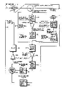
Fig. 1 is a block diagram of an output control
circuit for a nonlinear power amplifier with a continuous
output signal according to the invention; and
Fig. 2 is a block diagram of the output control
circuit with a discontinuous output signal according to the
invention.
DETAILED DESCRIPTION OF ILLUSTRATIVE EMBODIMENTS
A new digital cellular modulation standard, known
as ~/4DQPSK modulation, requires simultaneous amplitude
modulation (AM) and quadrature phase-shift keying modulation
(QPSK) of a transmitted signal. Preservation of this
amplitude and phase information is crucial in a cellular
transceiver. Thus, unlike
~~U~~~~
-5-
prior analog cellular systems, where only the frequency of the
modulated signal needs to be preserved and therefore a
nonlinear amplifier can be used directly, a nonlinear amplifier
cannot be used directly in such a digital cellular system
because the amplitude and phase information would be lost or
grossly distorted.
The circuit of Fig. 1 enables a nonlinear radio frequency
(I2F) amplifier 10 to be used in a digital cellular transceiver.
Basically, a control circuit 11 is connected between the output
and the gain control input of the nonlinear amplifier 10,
forming a feedback loop. The control circuit 11 includes an
output sampling means 20, a first signal selection means 15, a
detection means 70, a first sample-and-hold circuit 90, a
second sample-and-hold circuit 100, and a difference amplifier
110.
The output of the nonlinear amplifier 10 is sampled by the
output sampling means 20 which produces a sampled output
signal. The sampled output signal is fed to a signal selection
means 15, which also receives an input baseband signal. The
input baseband signal may be generated, for example, from voice
and data information by simultaneous amplitude modulation (AHt)
and duadrature phase-shift keying modulation (QPSK).
The signal selection means 15 modulates the sampled output
signal and i:he input baseband signal to generate a modulated
sampled output signal and a modulated input baseband signal,
respectively, which are alternately transmitted to the
detection means 70. The detection means 70 produces a detector
output signal representative of the power level of either the
modulated sampled output signal or the modulated input baseband
signal. The detector output signal is stored alternately by
either the first 90 ~r sect~nd 100 sample-and--hold circuit. The
difference amplifier 1.10 then determines the difference between
the stored detector output signals and transmits this
difference as a signal which controls the gain of the amplifier
10.
~~~~~5~
By so adjusting the difference signal fed to the gain
control input, the RF output signal of the nonlinear amplifier
is also adjusted to linearly track changes in the input
baseband signal. Specifically, the control circuit il adjusts
the gain of the nonlinear amplifier 10 in such a way that any
changes in the input baseband signal result in a proportional
change in the RF output signal. The only restriction is that
this adjustment in the output of the nonlinear amplifier l0
must occur at a rate which is faster than the rate at which
changes in the input baseband signal are received, so that the
control circuit il has enough time to adjust the output of the
nonlinear amplifier l0. In other wards, the bandwidth of the
control circuit 11 must be greater than the bandwidth of the
input baseband signal.
More p~rti.cularly, the nonlinear amplifier 10 in fig. 1
has a radio frequency (RF) input, a gain control input, and an
RF output. The RF input receives an RF carrier signal, and the
gain control input receives a difference signal from the
difference amplifier 110.
The output sampling means 20 samples the RF output signal
from the nonlinear amplifier 20, to generate a sampled output
signal consisting of a voltage which is proportional to the
power level in the RF output signal. Typically, a directional
coupler is used as the output sampling means 20.
The sampled output signal is then supplied to the signal
selection means 15. The preferred implementation of the signal
selection means 15 differs, depending upoxa the type of RF
output signal which is normally elected. With a continuous RF
output signal expected, as shown in Fig. 1, the signal
selection means 15 includes a first modulation means 30, a
second modulation means 40, a first enabling means 50, and a
second enabling means 60. With a discontinuous RF output
signal expected, as shown in Fig. 2, the signal selection means
includes a high pass filter 1~0 and a selection means 150.
The signal selection means 15 of Fig. 2 is explained in greater
2~~~'~~ Q
_7_
detail below.
Returning to the embodiment of Fig. 1, the first
modulation means 30 receives the sampled output signal and a
low frequency modulation signal and outputs a modulated sampled
output signal, which serves as a lower frequency version of the
sampled output signal. A lower frequency signal is more
desirable because it generates less noise in the system.
Additionally, the higher the frequency of the sampled output
signal becomes, the more expensive the detector diode in the
detection means 70. Typically, the low frequency modulation
signal is a square wave. Tt should have a frequency at least
twice as high as the frequency of the first and second enabling
signals used by the enabling means 50 and 60. This guarantees
that the modulated sampled output signal is properly sampled
according to the well-known request criteria.
An amplifier 120 may be connected to 'the output of the
first modulation means 30, to increase the signal level of the
modulated sampled output signal.
The modulated sampled output signal is in turn received by
the first enabling means 50. The first enabling means 50 also
has an input for the first enabling signal. Then the first
enabling signal is received, the first enabling means 50 is
enabled and the modulated sampled output signal is transmitted
to the detention means 70.
The signal selection means 15 also includes a second
modulation means 40 and a second enabling means 60. The second
modulation means 40 receives the input baseband signal, the low
frequency modulation signal, arid possibly a radio frequency
carrier signal.
The input baseband signal is typically generated by a
circuit (not shown) which impresses digital baseband voice and
data information on to a carrier signal using the desired
digital modulation and then combines it with an output power
level control signal. The low frequency modulation signal fed
to the second modulation means is the same low frequency
~~~~"r'~~3
modulation signal fed ':.o the first modulation means 30. Again,
the low frequency modulation signal has a frequency at least
twice as high as the frequency of the second enabling signal
and is typically a square wave.
A radio frequency carrier signal may also be input into
the second modulation means 40 for additional modulation if the
detection means 70 is sensitive to radio frequency signals. In
particular, the detection means 70 may be unable to detect the
output power level of the modulated input baseband signal.
Thus, to enable the detection means 70 to operate accurately, a
radio frequency carrier signal may be fed to the second
modulation means 40 For additional modulation. The particular
radio frequency carrier signal used for the modulation will be
whatever is necessary to make the detection means 70 operate .
properly.
The modulated input baseband signal is received by the
Second enablimg means 60, which also receives the second
enabling signal. When the second enabling signal is asserted
true, the second enabling means allows the modulated input
baseband signal to be transmitted to the detection means 70.
The first enabling signal is exactly the complement, or
180 degrees out of phase with, the second enabling signal, to
insure that the two enabling means 50 and 60 are never enabled
at the same time.
The detection means 70 receives the output of both the
enabling means 50 and 60. Typically, the detection means 70 is
a half wave rectifier such as a detector diode. Detector
diodes have a forward direct current ~D~) voltage drop that is
affected by changes in temperature, and accordingly cause the
output power level of the amplifier to fluctuate. However,
since the modulated sampled output signal and the modulated
input baseband signal are alternately supplied to the same
detector diode, they are therefore affected by the same
changes. When the difference between the two signals is
determined by the difference means 110, and changes induced in
each signal cancel each other out. Thus, any temperature-
induced offset introduced by the detection means 70 is not a
concern.
An amplifier 120 may be connected to the output of the
detection means 70, if the level of the detector output signal
is inadequate.
The envelope detection means 80, connected to the output
of the detection means 70 (or the amplifier 120, if included),
removes the low frequency modulation signal from the detector
output signal. The envelope detection means 80 is not
necessary if the low frequency modulation signal is a square
wave, because the first and second sample-and-hold circuits are
then able to detect the signal peak directly.
The first and second sample-and-hold circuits 90 and 100
are connected to the output of the envelope detection means 80.
The first enabling signal received by the first enabling means
50 is also received by the first sample-and-hold circuit 90.
When the first enabling signal enables the first enabling means
50, it also causes the first sample-and-hold circuit 90 to
sample the output of the envelope detection means 80.
Likewise, the second sample-and-hold circuit 100 receives the
second enabling signal to enable the second enabling means 60
and cause the second sample-and-hold circuit 100 to sample the
output of the envelope detection means 80. The first and
second sample-and-hold circuits 90 and 100 never sample the
envelope detection means 80 simultaneously. Preferably, the
first and second sample-and-hold circuits 90 aid 100 enter the
sample made at the end of the cycle ef the first and second
enabling signals. The first and second sampled signals are
stored as voltages in the first and second sample-and-hold
circuits 90 and 100.
A difference amplifier 110 is connected to the outputs of
the sample-and-hold circuits 90 and 100, to generate a
difference signal from the held first and second sampled
signals. An amplifier 120 and filter 130 may be connected to
-10-
the output of the difference amplifier 110, if necessary, which
adjust the level and bandwidth; of the difference signal. The
filter 130 should have the same bandwidth as the input baseband
signal.
The difference signal is then'fed to the gain control
input of the nonlinear amplifier lo, thereby adjusting its
output level.
Fig. 2 is a block diagram illustrating the control circuit
11 which controls nonlinear amplifier 10 far a discontinuous RF
output signal. The reference numerals used in Fig. 2
correspond to those found in Fig. 1 for similar blocks.
In the embodiment shown in Fig. 2, the discontinuous RF
output signal may be obtained in at least two ways. A
discontinuous RF signal may be supplied to the RF input of the
nonlinear amplifier 10; alternately, the nonlinear amplifier
may be systematically turned on and off.
The output sampling means 20 connects the output of the
nonlinear amplifier 10 to the signal selection means 15. In
the embodiment, the signal selection means 15 includes a high
pass falter 140 and a selection means 150. The output sampling
means 20 samples the discontinuous RF output signal from the
amplifier 10, and provides a sampled output signal to the high
pass filter 140. The high pass filter 140 then forwards a
filtered sampled output signal to the detection means 70:
As in the embodiment in Fig. 1, a second signal path in
the signal selection means 15 includes the selection means 150.
The selection means 150 receives the input baseband signal and
a zero level signal that indicates when the RF output signal is
at a zero power level. When the zero level signal is so
asserted, the selection means 150 allows the input baseband
signal to be fed to the detection means 70.
The detection means 70 is connected to the high pass
filter 140 and the selection means 150, and provides a detector
output signal indicative of the power level of the signals fed
to its input. Thus, when the RF output signal, and hence the
~~8c~7~ ~
sampled output signal, is at a zero power level, the input
baseband signal from the selection means 150 is transmitted to
the detection means 70. An enabling means, or switch, to
control when the sampled output signal is supplied to the
detection means 70 is not necessary for this embodiment.
An amplifier 120 may be connected to the output of the
detection means 70, if the level of the detector output signal
is inadequate.
The first and second sample-and-hold circuits 90 and 100
are connected to the outgut of the detection means 70, as per
the Figure 1 embodiment. When the sampled output signal is not
at a zero power level, then the first sample-and-hold circuit
90 samples the output of the detection means 70; otherwise, the
first sample-and-hold circuit remains in a hold mode. When the
sampled output signal from the nonlinear amplifier 10 is at a
zero power level, then the second sample-and-hold circuit 100
samples the output of the detection means 90. The first and
second sample-and-hold circuits 90 and 100 never sample the
detection means 90 at the same time.
The difference amplifier 110, amplifier 120, and filter
130 operate to control the gain of the nonlinear amplifier 110
as in the embodiment of Figure 1. The foregoing description
has been limited to a specific embodiment of this invention.
Tt will be apparent, howe-,er, that variations and modifications
may be made to the invention, with the attainment of some or
all of its advantages. Therefore, it is the object of the
appended claims to cover all such variations and modifications
as come within the true spirit and scope of the invention.