Note : Les descriptions sont présentées dans la langue officielle dans laquelle elles ont été soumises.
WO 92/03589 . PCI'/US91/06061
~3 20~96~4 ~
~IET~OD OF IMPROV:I:NG ION FLtJ~C DISTl~IBtJ~ tON
FOR~ITY ON A 8lJBSTR;~E
;~ The present invention relates to sputter
coating, particularly bias sputter coating, and
more particularly, to a control of ion flux
distribution uniformity in bias sputter coating
~`' applications, particularly in magnetron enhanced
bias sputter coating applications.
s~k~round o~ the Invention:
Sputter coating is a process carried out
,; in a vacuum chamber which is filled with a
generally chemically inert gas in which a substrate
is coated with a material for a target of
sputtering material subjected to a negative
electrical potential with respect to the chamber
wall or other anode. The potential gradient
~ ~ adjacent the target surface causes electrons to be
- emitted from the target which, on their way to the -~
; chamber anode which is usually formed in part by
the grounded chamber wall, strike and ionize some
of the inert gas. The positive ions formed are
then attracted to the negative target which they
strike, transferring momentum to the target
': '
'
- . . . .: , . . .. .
,., . . . , . . . , . . : .
.. . ... . . .. . .
' ' ' ' ' . , " , "' '" ' ," '.' ,' , ' :
.
. : .,: :
.
s,W092tO3589 2 Q 8 9 6 4 ~ : ` PCT/U591/06061
material, and ejecting particles of the material
from the target surface. The substrate to be
coated, which is positioned in th~ chamber usually
with its surface facing the target, receives some
of the ejected particles which adhere to and coat
the substrate surface.
With magnetron sputtering, a magnetic
field is formed over the target surface, usually
including magnetic field lines parallel to the
taryet surface, and, in many applications, in the
form of a closed magnetic tunnel. The magnetic
`~ field causes the electrons emitted to move in
curved spiral paths which trap them in regions
~ proximate the target surface enclosed by the field,
- l5 thereby increasing the rate of electron collisions
with gas atoms, which in turn increase the
ionization of the gas and the efficiency of the
sputtering process.
In the commonly assigned and copending
U.S. patent application Serial No. 07/339,308,
filed April 17, l989, entitled "Method and
Apparatus for Sputter Coating Stepped Wafers",
expressly incorporated herein by reference,
,............................................................................ ..
a sputter coating apparatus and method are
disclosed in which a concave annular target is
provided with concentric annular electromagnets
,~,
which cause the formation of a pair of concentric
~ W092/03~89 2 ~ 8 9 6 4 4 PCT/US91/06061
plasma rings. The plasma rings are alternately
enexgized by alternately 5upplying current to
energize the magnet coils while the target power
leveL is switchsd in synchronization with the
switching of the current to the magnetic coils.
~, This causes different rates of sputtering from
inner and outer concentric regions of the target
surface, with the sputtering from each region
causing different distribution characteristics of
the sputtered material deposited on the substrate
or wafer being coated. Varying the relative
parameters af~ecting the energization of the two
target regions provides control of coating
uniformity on the substrate surfaces, which is
especially important on the differently facing
surfaces of stepped semiconductor wafers. The
aforereferenced patent application particularly
describes effects on the coating caused by thie
targèt geometry and by the electrical parameters
relating to the energization of the target and
~ .;
plasmas.
In bias sp11ttering, a voltage which is
negative, but less ne~ative than that imposed on
. .............................. . .
the target, is applied to the substrate being
coatedi. This bias voltage causes a certain amount
. " .
of "back sputtering~', or sputtering from the
sputter coating which has been deposited on the
' .
'';: : ' ~
: . . : . . . . .
, ... . ..
W092/03~89 PCT/US91/06061
2089~ 4 _ ~
substrate surface, due to the impingement of ions
produced by electrons emitted from the substrate.
Frequently, however, particularly where the
sputtering target is annular with an annular or
other closed magnet trap over its surface, pole
-~ pieces behind the target produce magnetic fields
~ ~ .
which shape "primary" plasmas near the target
surface and produce a fringing field in the
- vicinity of the substrate surface which is non-
unifor~. Components of the fringing ~ield so
~, produced are perpendicular to the substrate surface
in certain regions, as fox example, at the center
on the axis of the target magnet center pole. This -~ -
fringing field and other portions of the electric
and magnetic fields tend to concentrate regions of
. .,~: . .
"secondary" plasma formation which produces
a secondary ion flux bombaxdment of the substrate.
,;:
~ The result is often an undesired non-linear
,~,~ . .
distribution of ion flux on the substrate surface.
~ solution to the problem of non-uniform
ion 1ux distribution on the surface of the
; ~
substrate is described in the commonly assigned
U.S. Patent No. 4,871,433 entitled "Apparatus for
Improving the Uniformity of Ion Bombardment In a
Magnetron Sputtering System". In that patent, the
use of a secondary magnet behind or around the
substrate having certain charac~eristics is
,','
,~ .
,., : ; .. . : ,
,
W092/03589 2 0 8 9 6 4 4 PCT/US91/-6U61
.~ described. The ~econdary ma~net, or countermagnet,
modifies the fringing field prod~ced by the cathode
. or targat primary magnet to render the ion flux
uniform on the substrate. While effective, the
-~ 5 apparatu5 in that patent is somewhat specific to
-; the cathode and cathode magnet arrangement, is .
large and difficult to fit into many processing
chamber arrangements, and often must be replaced .:
when the target magnet scheme is changed.
Furthermore, the level of ion flux which is
:
provided with such a countermagnet system is
. limited. ..
. ~ .
.; Certain sputter coating devices of the ~ :-
.- prior art which employ annular sputtering targets :
; 15 employ the use of an anode at the target center.
The anode is provided to avoid heating of the wafer
. due to secondary electron bombardment of the wafer.
Such targets are provided with what is called a
dark space shield which surrounds the target at its
.~ 20 outer rim to absorb electrons which stray.from the : :
, , :
plasma, preventing them from striking the substrate .
~ surface. ThP anodes provided at the target centers
.~ are maintained at the same grounded or other anode
potential of the dark space shield to absorb stray
electrons near the target center. Such electrons,
:~ if nat kept from the substrate, ~hile heating the
surface, are thought to collact on the surfaces of . .. -
~: .
~ ..
';'''' :'
,.' : . ' . . , ', . . . ,.. , ~ .. ~ ,., , ; . . .. .
.
., .. ... ;,~, . ' . , .. .. .. :~, . ..
,: . , : , .
W092/03589 ~, PCT/US91106061
2 0 8 9 6 4 4
layers dPposited onto conductive substra~es,
even-tually causin~ a breakdown of the no~-
conductive material and damage to the substrate
surface. These prior art electrodes were also
placed to critically intercept some of the plasma
trapping field lines, generally reducing their
effectiveness.
- Summary of the Invention:
It is an objective of the present
invention to provide uniform ion flux distri~ution
on the surface of a substrate wafer being coated in
~ .
;~ a sputter coating process, particularly a bias
sputter coating process performed with a magnetron
enhanced sputter coating device.
-~ 15 It is a particular objective of the
present invention to provide ion flux distribution
uniformity on a substrate surface with a method
that is sufficiently flexibile to accommodate
target assemblies of various magnetic, electrical
and geometric configurations, and can accommodate
target energization methods which change during the
sputtering process being performed.
According to the principles of the
~, present invention, a sputter coating apparatus is
provided with an electrode disposed generally
remote from the outer edge or rim, and preferably
on the center line, of the target, near the target
,. . .
W092/03589 ~ ~ 8 9 ~ ~ ~ PCT/US91/06061
- 7 -
surface. The electrode is biased to a voLtage
which differs from, and is preferably negative wïth
respect to, the sputtering chamber anode and the
potential of the dark space shield surrounding the
~; 5 target rim, but which is not as negative as the -~
potential on the target itself. Preferably, the
central electrode i5 biased at a negative voltage
which lies between a negative voltage greater in
magnitude than zero and a negative voltage of about
twenty volts (-20 v.), often preferably in the
range of about negative eight (-8 v.) volts. This
compares with a corresponding target voltage which
is usually at an approximate n~yative potential of
several hundred volts.
Further, in accordance with the preferred
embodiment of the present invention, a switched two
plasma annular target with alternately energized
concentric inner and outer annular plasma rings is
provided with a central electrode which is
energized at a negative potential, particularly
when the outer plasma is energized. When energized
;~ at a substantially less negative potential than the
.:.~ , . .
~ tar~et, the ceTItral electrode absorbs stray
. . .
electrons which, during energization of the outer
plasma, are too remote from the outer darX space
shield to be captured by it, thereby reducing stray
electron bombardment of the target from
.'`
' '~ .
,,
, , ' , . . : . . ' . : : ,,: . .
W092/03589 PCT/US91/06061
2 ~ 8 9 energization of the outPr pla5ma. The energization
of the central electrode is, however, switched to a ~-
more nearly ground potential when the inner plasma
is energized bacause stray electrons from the outer
- 5 plasma are not required to be captured in the
;~ center of the target.
Further, according to the present
invention, the voltage of the central electrode is
`~ maintained at a negative value which, it has been
found, is effective to cause positive ions to be
attracted toward the electrode. More importantly,
an effect of the biased central electrode, so
positioned, is that it renders the distribution of
ion flux on the substrate surface uniform without
the need for a specially configured countermagnet
structure near the sub~trate.
The optimal elect:rode voltage is
` determined preferably empirically by adjusting the
electrode voltage and measuring ion flux across the
surface of the substrate. The negative voltage
applied to the central electrode is different with
different targets and different energization
schemes of the target. By use of the negatively
biased central electrode, the negative voltage may
be changed as the conditions are changed to
optimize the shapes of the electric fields to
, . ..
. W092/03589 2 0 8 9 ~ 4 4 PCT/US91/06061
_ 9 -- ! `. .:
thereby affect and maintain ion distribution ` ;
uniformity on the substrate surface being coatedO
These and other objectives of the present
invention will be more readily apparent from th~ :
; 5 following detailed descri~tion of the drawings in
~ which:
',~ ' ' ~', .
.'' ' .
'. ...
~ ' .' .
., .
i '' '
~- ,
: .
, . . .
'" ,:-,.
' ''
. .
~''.'
:;'',~ ' . ,
, ........................................................................ . .
,
~i~ ",
, , , : . : .. : : . . .
~: , , , :, . ,
W092/03589 PCr/US91/0606l
2~ 4~ lo- -
~- Bri~f Deqcri~tion of the Dr~inqs:
Fig. 1 is a cross-sectional view of a
processing chamber of a sputter coating apparatuS
according to principles of the present invention,
~;~ 5 Fig. 2 is a diagram illustrating the
electrical circuit arrangement of the embodiment of
Fig. 1:
Fig. 2A is a diagram similar to Fig. 2,
- illustrating an alternative application of the ,
present invention.
Fig. 3 is a diagram illustrating the
waveforms or timing of the switching of the target,
- wafer and electrode voltages with the circuit
- arrangement of Fig. 2.
Fig. 4 is a comparative graph
illustrating ion flux distrlbution according to the
.. ~
~- present invention.
: ~ .
, .
." .
~ . ,i................... .
W092/03589 2 0 8 ~ 6 4 ~ PCT/US91/06061
Detailed Description of Drawinqs
Magnetron sputtering devices of the type to
which the present invention relates are described in
the following commonly assigned U.S. patents and
copending patent applications which are hereby
expressly incorporated in their entirety into this
application by reference:
U.S. Patent No. 4,853,033 for ~'Cathode
Target Design for a Sputter Coating Apparatus";
U.S. Patent No. 4,871,433 for "Apparatus for
Improving the Uniformity of Ion Bombardment In a
Magnetron Sputtering System";
U.S. Patent Nos. 4,909,675 and 4,915,564
entitled "Method and Apparatus for Handling and
Processing Wafer-Like Materials": and,
, " , .
U.S. Patent application Serial No.
07/339,308, filed April 17, 1989 entitled "Method and
. Apparatus for Sputter Coating Stepped Wafers."
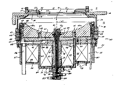
Fig. 1 illustrates, in cross-section, a
sputter coating processing chamber 10 of a sputter
.: ,
I coating apparatus according to principles of the
present invention. The chamber 10 is a portion of the
sputter processing apparatus disclosed in U.S. Patent
~; 4,909,675. The processing chamber 10 is a vacuum
A ~, . . .
~ processing chamber formed of an isolated section of a
,~z main chamber 11. The main chamber 11 is isolated from
the atmosphere of the machine environment 12 by a
, ' " '~
:, .
. . , ~ . . ... ~ . , . , .. , : .
,, ', ~' : , .. .
'. '': ' ' '' , " .: ,. ., '' ,' . ' ' :
, : ' , : , : .
W092/03589 PCT/~S91/06061
20~ 12- ~
plenum wall 14. The processing chamber 10 is capable
of communicating with the main chamber 11 throughout
opening 15 in the plenum wall 14. The opening 15 is
generally circular. The processing chamber 10 is
capable of being selectively isolated from the main
chamber 11 by the selective movement of a processing
chamber back plane section 16 against a portion of a
disk shaped rotary wafer transport member 17 clamping
the transport member 17 between the backplane section
16 and the plenum wall 14 in a sealing relationship,
thereby enclosing a back plane space 19 within the
processing chamber 10 and isolating the processing
chamber lO from the main chamber 11.
Opposite the backplane section 16, on the
front plane side of the transport member 17, the
processing chamber 10 is isolated from the machine
environment 12 with a cathode assembly module 20
mounted in a vacuum sealing relationship against the
plenum wall 14 surrounding the opening 15. The module
20, or processing chamber frontplane section, cooper-
ates with the backplane section 16 and the transport
member 17 to form the sealed isolated processing
chamber which is isolated from both the main chamber
11 and the machine environment 12. Within the pro-
cessin~ chamber 10 is a workpiece 21 in the form of a
flat silicon wafer or disk which has the surface 22
upon which a coating is to be deposited in a sputter
W092/03589 2 0 8 9 6 4 4 PCT/US91/06061
; ~ -13- '`
., .
coating process to be performed within the processing -.
chamber 10. The wafer 21 is held by a set of clips or
: . other retaining devices 24 in a wafer holder 25
resiliently carried by the transport member 17. The
` transport member 17 is rotatable within the main :
~; chamber to bring the holder 25, and the workpiece or
wafer 21 into alignment with the hole 15 so that the
~: processing chamber lO can be formed around the wafer
..
21 on the holder 25 by transverse movement of the
~: backplane section 16 to move the member 17 against the
plenum wall 14. (The transport member portion 17 is a
; . transversely movable ring carried by a rotatable index
plate which is not shown.) In this preferred embodi-
. ment, the wafer 21 is supported in a plane perpendicu- :
, lar to, and concentric with, a central axis 27 of the
3', main chamber 10, which is also concentric with the
:~:` . hole 15 in the plenum wall 14. Surrounding the wafer
21 on the holder 25 is a disk 29 which at least
. partially protects the holder 25 from an excessive
~,~ accumulation of coating intended for but which missed, .
the surface 22 of the wafer 21. Details of the
~- sputtering apparatus of which the processing chamber -~
10 is a part including particularly details of the
: wafer transport 17, wafer holder 25, and back plane
. section 16, are described and illustrated in the U.S.
Patents 4,909,675 and 4,915,564 incorporated by
reference above.
,.; :
,,',
,.',' '
,, , : . : . -
, " ' ' , ;~ . .' '':
', , " ', ' ' "' ' ' '' .'' ~: ' :
!' ' ' : . , :
,,
WO9~/03S89 . , PCT/US91/0606~ .
~089~ 14- . ~
The cathode assembly module 20 includes two
assemblies, a removable cathode assembly 30 and a
fixed assembly portion 31. The fixed assembly portion
31 is an annular enclosure rigidly mounted in sealed
relationship against the plenum wall 14 surrounding
the opening 15. It includes a cylindrical metal side
wall 33 of the chamber 10 which i5 electrically
grounded to the frame 14 of the plenum, a wafer holder
shield 34 which surrounds the opening 15 and a chamber
door frame assembly 35.
The cathode assembly 30 is mounted to a
;: hinged door assembly 37 which removably but sealably
supports the cathode assembly 30 to the fixed assembly
. .~.~ .
31. The cathode assembly.30 carries the sputtering
target 40, which is an annular concave target having a
continuous smooth concave sputtering surface 41. The
assembly 30 supports the target 40 with its axis in
alignment with the axis 27 of the chamber 10 and with
its sputtering surface ~1 acing the surface to be
coated 22 of the wafe'r 21.
The target 40 is supported in a target
holder or nest 42 having a generally circular back
plate 43 concentric with the axis 27. The target
holder 42 has an outer cylindrical wall 44 and an
upstanding cylindrical midwall 45. The outer wall 44
surrounds the outer rim of the target 40. The target
40 has an outer cooling surface which, when the target
. , .
: " ' ' " '' ',
,
: .,
W092/03589 2 ~ 8 ~ 6 ~ ~ PCT/US91/0606~
-15-
40 is mounted in holder 42 and expanded to operating
temperatura, conforms to and lies in close cooling
contact with the inner surface of the holder 42. ~n
annular groove 47 on the back of the target 40 lies in
partial contact with the midwall 45 of the holder 420
The target holder or nest 42 has a plurality of
annular grooves 48 in its back surface and annular
grooves 49 on the outside of its outer wall 44 for the
circulation of cooling liquid, which is generally
water, to remove heat generated in the target 40
during sputtering by cooling the heat conductive
target holder 42. The shapes of the surfaces of the
target 40 are preferably such that all the target 40
is capable of being formed by turning block of sput-
tering materlal on a lathe. The target holder 40 is
made of a heat conductive and electrically conductive
material, preferably hard tempered OFHC copper or -~
Alloy 110. The target 40, when operationally heated,
expands and preferably plastically deforms into a
shape which conforms tightly to the interior cavity of
the holder 42 and thereby cooperates with the holder
42 to conduct heat thereto. The cooperation of the
holder 42 and the target 40 are preferably as ~ ;
described in U.S. Patent No. 4,871,433 incorporated by
reference above.
The target assembly 30 is provided with a
maynet assembly ~0 which preferably includes a pair of
'
, ~ ' ', . ' '
'' ' ' " ' '. " ' ' ' ,
~ ,. . .
W092/03589 PCT/US91/06061
.. : i
~ %~9~ 16- ~1
concentric annular magnets 51 and 52, preferably
electromagnets having annular inner and outer windings
53 and 54, respectively, lying concentrically in a
plane behind the target holder 42 and centered about
and perpendicular to the axis 27. A rigid ferrous
material, such as 410 annealed stainless steel, forms
the structural support of target assembly 30 and
constitutes the magnetic pole pieces of the magnets 51
and 52. This ferrous material includes a circular
center plate 56, which forms the planar rear support
of the assembly 30 and sustains the transverse mag-
netic field between pole pieces of the magnets 51 and
52. A cylindrical outer pole piece 57 is welded to
the pla~e 56 at the outer edge thereof to stand
upwardly therefrom and to surround the outer wall of
the holder 42. A target outer retainer ring 58, is
bolted to the upper edge of the outer pole piece 57,
so as to rest on an outer annular lip 40a of the
target 40 to retain the target 40 in the nest 42. The
upper exposed surface of the outer pole piece 57 and
ring 58 is shielded by a metal dark space shield 59,
which prevents sputtering of the pole piece 57 or
retainer ring 58. The dark space shield 59 is rigidly
secured to the chamber wall 33 and thereby electrical-
ly grounded.
An inner cylindrical pole piece 61, having
as its axis the axis 27, projects through the inner
..:
- . .
, ~
.
' ' - . ,~ ' . . ,
- . , ~ . , .
" ' ' ', ' ' ' ~, ' '' ' ':
W092/03589 2 ~ 8 9 ~ ~ ~ PCT/US91/06061
~ 17-
.~ , ,:, . .
rim of the target 40. This pole piece 61 is threaded'
through the center of the holder 42 below the target
40, and has threaded thereon, above the target 40, a ,-~
center retainer nut 62 which retains the target 40 at
its center hole. The center pole piece 61 has bolted
. .
to the bottom end thereof a pole cap assembly 63. The
pole cap assembly 63 includes a circular inner plate
Ç4, a cylindrical lower middle pole piece 65 welded at ''
its base to the outer edge of the plate 64, an annular
outer plate 66 welded at its inner edge to the outside '':
of the lower middle pole piece 65, and a lower cylin- '
drical outer pole piece 67 welded at its base to the :
outer edge of the annular plate 66. The lower outer
pole piece 67 has bolted to its upper edge, base 68 of ;~:
outer pole piece 57. The components 64, 65, 66 and 67 ; :
of the pole cap 63 have a common axis lying on the . ':',
axis 27 of the chamber 10. '
The middle cyl,indrical pole piece 65 under~
lies the annular groove 47 in the back of the target '
40, and projects either in a continuous annular ring
or at spaced intervals through the plate 56 into a
recess 69 in the back surface of the holder 42. A
ring 69 of rigid ferromagnetic material and having
approximately the same diameter as that of the middle
pole piece lies, and is embedded within, the annular
groove 47 in the back surface of the target 40. The
upper end of the middle pole piece 65 lies in the
,
.
..
... . . . . . . . . . .
, . . . . .
,:, ................................ , ":. ' ' , . ,
: ' : , . ,; , , . , , , , . ,, . . :,
,' ,. ~ ' .: :. . ,',
` WO 9~/03589 PCltUS91/06061
-18-
2~8~4 annular groove through the surface of the backplate 56
close to the ring 69a. The ferromagnetic ring 69
surrounds the midwall 45 of the holder 42 in the
groove 47 in the back of the target 40.
The middle pole piece 65 together with the
ring 69a form a pole piece which the inner and outer
magnets 51 and 52 have in common. The ring 69a is
magnetically coupled to the middle pole piece 65 so as
to extend tha effective pole piece at the annular
groove 47 of the target 40 to very near, but beneath,
the surface 41 of the target 40. In that the ferro-
magnetic ring 69a is of a rigid ferromagnetic mate-
rial, it is substantially stronger structurally than
the soft copper of the holder 40 is made of a material
which expands less when heated. As such, it serves to
structurally reinforce the midwall 45 of the target
holder 42 against radial expansion caused by the
heating of the target 40, thereby also restraining the
;; tarqet 40 against radial thermal expansion.
Concentrically mounted at the top of the
- center pole piece 61 is a central electrode 70,
electrically insulated from the pole piece 61 by a
ceramic washer 71. The center pole piece 61, the
, ,;
target 40, the holder 42 and the entire center plate
56 and pole cap assembly 63 are energized to the same
cathode potent~al. Accordingly, the assembly 30 is
'~
.
,
.
'~ ,
,: - . , . .,, , . . . . . . - . .
... , .: . . . ., :~ : .
'' ,',',': ' ' ' ,' ' '"' ." :" '- .., :' " ~ ', '' ' ' ' '' ' ' : ' ' '. : '', ,
"~, . . .. ~. . . . .
... . . . . . .
:, : , ' ' ' : '
` W092/03589 2 ~ ~ ~ 6 ~ ~ PCT/US91/06061
. -19~
insulated from the grounded fixed assembly 31 by a
Teflon insulated annular spacer 73.
A center pole cap 76 is fixed to the bot~om
of the pole cap assembly 63, concentric with the axis
27. The cap assembly 63 supports an outer cooling ,:
fluid tube 77 which extends vertically through a bore
78 in the central pole piece 61 to the electrode 70
with which it makes electrical contact. The tube 77
is electrically conductive and insulated from the cap :
76 to provide for the eneryizing of the electrode 70 :-
at a potential which is different from the target -40 .
or the grounded chamber wall 33. Mounted to the .
bottom of the cap 76 is an outlet tube assembly 79 for -
transm.itting cooiing fluid from the tube 77. An inlet
assembly 80, connected to the base of the outlet~: -
assembly 79 supports an inlet tube 81 which extends
through the center of the tube 77 to the electrode 70
to supply cooling fluid thereto. A water inlet 83 and
outlet 84 are provided in the inlet assembly 80 and
outlet assembly 79 respectively. Similarly, cooling
passages 85 are provided in the plate 56 for commu-
nicating cooling water ~rom passages 48 and 49 to a
cooling water outlet 86 in the plate 56. A cooling
water inlet 87 communicates water through a grinder
inlet duct to the passages 48 and 49 in the holder 42.
The elec~.-ical circuitry of the sputter
processing portion of the apparatus is illustrated in
, ' - .
,," ' ,,,
.. . .. . .. . .
, . . . :. .
': , ' ' . . ' . ,, .~ .
.. ..
: : ~ . , '
.
W092/03589 PCT/US91/OS061
2~8~44 -20-
the diagram of Fig. 2 which shows the Sputtering
chamber 10 with its wall 33 maintained electrically at
ground potential through a system ground connection
100. A target power supply 102 supplies energy at a
negative potential of, typically, several hundred
volts through conductor 104 to the target 40. This
voltage results in a flow of current manifested in
part as a flow of electrons from the surface 41 of the
target ~0 into a one or more plasmas 106, 108 main-
tained over the target surface 41 and by an ion flux
from the plasmas 106, 108 onto the surface 41 of the
target 40. The plasmas 106, 108 are ionized clouds of
the chamber gas formed as electrons collide with the
gas atoms stripping other electrons from them.
The wafer 21 is connected so as to be
maintained closer to ground potential but, for bias
sputtering, is biased so as to be substantially
negative relative to ground in the range of from 50 to
100 negative volts, -100 volts in the illustrated
example. The bias potential is supplied through a
conductor represented as line 110 from the power
supply 102. A current in the circuit through line 110
is a resultant, in part, of an emission of a small
quantity of electrons from the surface 22 of the wafer
21 and a secondary flow of ions onto the surface 22
, .
from a space 112 near the surface 22. The secondary
ions are the result of collisions of the electrons
, .
.,, '
,
, ', ,:
:: : ,. , , , . , ,, : . " , ,,
',,.,,: ., ' . : , ., ' ,: , ,
.,, , , ' . ' , .
' :,; , ' . . : '' ' . ' , . . : '':
W092/035~9 2 ~ ~ ~ 6 ~ ~ PCT/USg1/~606~
-21- -
emitted from the wafer 21 with gas in the space 112.
The current may also result, in part, from electrons
and ions striking the surface 22 of the wafer 21 ~rom
the regions of the plasmas 106 and 108.
The power supply 102 also is provided with
an output 114 for applying a potential to the central
electrode 70. This potential is preferably a negative
potential of from -0 volts to -20 volts or greater in
magnitude. Current through line 114 is a result, in
part, of electrons flowing onto the electrode 70 which
stray from the more negatively charged target 40 and
plasmas 106, 108 to which they return through the
conductor 104, completing the circuit. This current
is believed, however, to be more largely the result of
ions attracted to the electrode 70 from the plasmas
106, 108. Typically, this current is in the range of
- ,
from 10 to 100 milliamps. Similarly, some current
1OW in circuits through the conductors 104, 110 and
; 114 via the system ground 100 as a result of electrons
and ions striking the chamber wall 33~ the dark space
shield 59 and other grounded components of the chamber
., 10.
~ ~ Also provided are one or more magnet power
-- supplies 115 for activating the magnet windings 53 and
~; 54 by supplying current to them through leads 116, 118
respectively, and control circuitry 120 for control-
, ",
ling the operation of the power supplies 102 and 115
,' .~ .
.'' , ' .
: '
' . .
,, . ,,:
.
,' ., ,' , . . , ... ~: :
: :':
, ,', , ...... ; :, ,' , ,. '' ', ' .'
W092/03~89 ; PCT/US91/06061
2089 ~ 44 -22-
with control signals supplied through signal lines
represented as 122 and 124 respectively in Fig. 2.
The circuits 115 and 120 also have grounds connected
- to the system ground 100.
In the preferred embodiment of the inven-
tion, only one of the plasmas 106, 108 is energized at
a time. This is achieved by switching the current to
the magnet windings 53, 54 on and off alternately with
signals from the controller 120 through line 124 to
the magnet power supply 115. The currents to the
magnet windings 53, 54 are switched to different
current levels IT, Io and for differing "ON"-time TI
and To as represented by the graphs A and B of Fig. 3.
This causes the sputtering to alternate between two
respective annular regions 126, 128 of the surface 41
of the target 40 underlying the respective plasma
rings 106, 108. In synchronization with this
switching, the power level of the target 40 is
switched between two levels, PI, PO, as illustrated in
graph C of Fig. 3, so that the power is separately
maintained during sputtering from the respec~ive inner
and outer targe~ regions 126, 128. The control of the
:, .
switching of the power level at the output 104 of
power supply 102 is maintained by a signal on control
line 122 from controller 120.
In the performance of a sputter coating --
Gperation in a sputtering chamber 10, it is usually
:
. . .
. . . - . . . . . : . . .: , . .. : . : . . . ::.. ..
, . . , ., :
, . .. . ,, : ,. , . . ~ . , . : ..: , . : , . . .
::'' : '
.
''' ' . ., . ' ': . ', . '' .: ' : :
. W092/0358~ 2 ~ 8 9 ~ ~ ~ Pcr/us9l/0606l
-23-
- .' ''
desired that electrons emitted from the surface 41 of
the target 40 be trapped and remain entrapped in the
plasmas 106, 108. The provision of the magnets 51, 52 ~ .
generate, when their coils 53, 54 are energized,
magnetic fields 131, 132 which form arched closed loop
magnetic tunnels in the shape of annular rings on the
target surface 41 as determined by the placement of
the concentric pole pieces 61, 65 and 67. This
applies to structures, such as in the embodiment shown
herein and more particularly described in U.S. patent
~ application Ser. No. 07/339,308 incorporated above,
; where the plasmas are alternately switched on and off,
or where they are energized simultaneously, such as
that described in U.S. Patent No. 4,595,482. It
further applies to single plasma structures such as
shown in U.S. Patent No. 4,673,~80.
Electrons which do not remain in the plasmas
move toward the less negatively charged components of
: the chamber 10, some of which strike and are absorbed
by the substrate 21. Electrons which strike the
substrate may result in currents which cause unwanted
heating of the substrate, or may collect, where the
substrate or a deposited layer of the substrate are
` non-conductive, building up charge and causing even-
tual voltage breakdown and damage to the wafer.
; To prevent stray electrons from striking the
; substrate, the dark space shield 59 is conventionall~
,
' .
, , , ,: , - . :
.
, . , , , ~ ~
,: ,' ,. ' . ~ , ' ` , ,' ' - ' .
,' ' " ' ' ` '', -~' , . '
. ' ,' ~ :' " '~ '
.
:' ', , ~ ' , ~ ,
W092/03589 PCT/U~91/~6061
-24-
2~9~ 44 provided and grounded to attract and absorb the
electrons. In that the shield 59 is remote from the
inner plasma of a two plasma target system such as
that of Fig. 2 or of U.S. Patent No. 4,595,482, a
central anode, such as electrode 70, will also absorb
electrons which stray near the center of the target
surface 4l, where the dark space shield may not be
able to attract and absorb them. This is usually done
by grounding the central electrode or otherwise
connecting it to the same potential as the dark space
shield~ With single plasma systems as shown in U.S.
Patent 4,673,480 and illustrated diagrammatically i~
Fig. 2A, where stray electrons near the center of the
.: .
target 4OA are too remote from the dark space shield
59A to be absorbed by it, a central anode 70A, con-
nected to the same potential as the shield 59A will
~ absorb the electrons near the wafer center.
In bias sputtering applications, particular-
ly magnetron enhanced of Flgs. 2 and 2A, where a -
negative bias is applied to the wafer 21, 21A through
~- conductors llO, llOA to cause the surface 22, 22A of
the wafer 2l, 2lA to be subjected to a secondary ion
, flux, uniformity of this ion flux on the substrate
must be maintained across the wafer surface 22, 22A so -
that uniform processing of the wafer coating is
achieved. Non-uniformity of this flux is caused, in
part at least, or is at least intensified by, the
:' ' ~ ':
:' ;:.
.-, :.
., - ,, .: - . . . . , : , . ~
-. , . . , ., , . . ~ -
.: . , . ~. . : . ~ .
.
, .. , : . ... ,, ,. : : :
,, . . . : : . :
.
" ' :' ''' ' ~.' ''
W092/03589 2 0 8 9 6 ~ 4 PCT/US91/06061
-25-
:
shape of the magnetic field in the vicinity of the
substrate surface 22 produced by the magnets 51 and
52. Correction of this phenomenon by the use of a
countermagnet at the substrate was taught in U.SO
Patent No. 4,871,433. Curves A and B of Fig. 4
illustrate the ion flux distribution on a substrate
with and without the countermagnet of U.S. Patent NoO
4,871,433.
In accordance with the present invention, a
central electrode, such as electrode 70, 70A, is
biased to a relatively small negative voltage, found
to be in the range of up to -20 volts in magnitude,
but adjusted to an optimum value. It has been found
that the value of this voltage or the electrode 70,
70A can be optimized so as to cancel effects which
produce non-uniform ion flux onto the substrates 21,
,.: .,
-~ 21A, thereby rendering it uniform without the need for
~ a countermagnet, and while still effectively absorbing
~ ,i
stray electrons near the center of the target 401 ~OAo
Furthermore, higher ion flux levels onto the substrate
can be maintained than with the countermagnet solu-
tion, as shown by curve C of Fig. 4. As a result of
the invention, the ion flux level is increased by 250%
over that of the countermagnet system. In addition,
the large countermagnet assembly which is often
difficult to fit into many sputtering devices, is
eliminated. Furthermore, the voltage of the central
,, ~
W092/03~9 ; PC~/US91/0606!
~89 ~ 44 -26-
electrode 70 can be more easily modulated than can the
countermagnet.
The optimum negative voltage bias to the
electrode 70, 70A varies with the other parameters of
the system, including both geometric and electrical
parameters. Accordingly, in the embodiment of Fig. 2,
the appropriate voltage of the electrode 70, which is
appropriate when the inner plasma 106 is energized,
preferably about zero, for example, is not the same as
that which is appropriate when the outer plasma 108 is
energized, which is approximately -20 volts in the
specific e~ample illustrated. Accordingly, as shown
in graph D of Fig. 3, the voltage on line 114 to the
, :
electrode 70 is switched between zero and -20 volts in
synchronism with the switching of the plasmas 106, 108
so that the voltage on the electrode 70 is optimum for
each part of the sputtering cycle in the switched
plasma system shown. Both the positioning and ths
` biasing of the central electrode 70, 70A affect the
~ ion flux distribution on the substrate and, according~
: :'
ly, may be changed to optimize the performance of the
electrode 70.
Curve D in Fig. 4, for example, illustrates
the ion flux distribution on the surface of a wafer 21
with a central anode 70 at ground potential as
compared with curve C which is the distribution with
the electrode 70 at -20 volts. Both curves are for an
,' .
,...
, .. :
" , . . . . . .. .
.. , ,. , , , . , ~:' '
'' . '' , . . : . : , , : : : ' .:
.. . . .
,, ' , : : i
W092/03589 2 0 8 9 ~ 4 ~ PCT/US9i/~6061
-27- ;
electrode 70 with the apparatus of Figs. 1 and 2
operating with only the outer plasma 108 energized.
Preferably, with each anticipated geometric relation-
ship of target 40, 40A, electrode 70, 70A and sub-
strate 21, 21A, the voltage applied to the electrode
70, 70A should be manipulated to adjust for condi-
tions, such as ion flux, at the substrate 21, 21A to
determine the optimum voltage settings for use during
operation.
; The spacing of the electrode 70, 70A is
preferably central to the surface of the target 40,
; 40A, generally on the target axis 27 in the embodi-
.,.,; - .
- ments where the target assembly is annular and the
components concentric, and between the target 40 and
the substrate 21, usually near to the target surface
41.
Having described the preferred embodiments
of the invention, it will be apparent to one skilled
, ,j
`- in the art that variations are suggested and can be
made without departing from its principles. Accord-
ingly, the followlng is claimed;
j
,
, ' ~ '
' ' ' .
.
, . " -