Note : Les descriptions sont présentées dans la langue officielle dans laquelle elles ont été soumises.
- ~ 2~7~
APPARATUS AND METHOD FOR GENERATING CHAOTIC SIGNALS
AND CHAOS DEVICE
BACKGROUND OF THE INVENTION
Field of the Invention
The present invention relates to a chaotic signal genera-
tor and a method of manufacturing the same, and a chaos
device.
A concept of "signal" used in this specification is
intendsd to cover an analog signal, a binary signal, binary
digital data and the like.
Description of the Related Arts
In the fields of mathematics, physics, computer science,
and others, theoretical and empirical research into chaos
is beginning to get lively. A chaos theory may be ~aid to be
possibly applied to data processlng, computer science such as
cellular automata, atmospheric conditions (e.g., weather
orecast), prediction of complicated natural phenomena such as
earthquakes, and others. In actual fact, however, it is still
in its infancy.
The following are documents concerning chaos.
"Chaos - Basis and Application of Chaos Theory" written
and edited by Kazuyuki Aihara, 1990, and published by Science
Co., Ltd.
: . . . : .. ; ........ ~
2 ~
"Mathematical Science" Nov. 1981 (No. 221), and May 19~9
(No. 221), Science Co., Ltd.
"Computer Today" July 1989 (No. 32), and Sept. 1989, (No.
33), Science Co. Ltd.
SUMMARY OF THE INVENTION
The present invention provides an apparatus and a method
for generating signals behaving chaotically with time which
are necessary for theoretical and empirical research into
chaos and applicable to display and the like.
A first aspect of the present invention is intended to
provide a basic apparatus (or a chaos device) and a method for
generating chaotic signals which include~ a nonlinear function
element and a linear function element.
A chaotic signal generator according to the first aspect
of the invention comprises a plurality of delay means for
delaying input signals in sequence by a predetermined period
of time; a nonlinear function means for converting through a
nonlinear function a signal derived from at least one of the
delay means; a coefficient means for multiplying signals
derived from the other delay means by a predetermined coeffi-
cient; an adding means for adding signals derived from the
nonlinear function means and coefficient means; and an ini-
tializing means for conferring initial values on the delay
means, or the nonlinear function means and the coefficient
means, or the adding means at the time of initiation of opera-
2 ~
tion; output of the adding means being fedback to the fore-
most one of the plurality of delay means.
This chaotic signal generator can be lmplemented by a
hardware architecture or by a computer software.
A chaos device according to the first aspect of the
invention which will be realized by a hardware circuit com-
prises a plurallty of delay circuits for delaying input
signals in sequence by an infinitesimal period of time; a
nonlinear function circuit for converting through a nonlinear
function a signal derived from at least one of the delay
circuits; a coefficient circuit for multiplying signals
derived from the other delay circuits by a predetermined
coefficient; an adding circuit for adding signals derived
from the nonlinear function circuit and the coefficient cir-
cuit; and an initializing circuit for conferring initial
values on the delay circuits, or the nonlinear function cir-
cuit and the coefficient circuit, or the adding circuit at the
time of initiation of operation; output of the adding circuit
being fedback to the foremost one of the plurality of delay
circuits.
A method of generating chaotic signals according to the
first aspect of the invention compxises the steps of retaining
a plurality of sequentially inputted signals in the order of
receiving the signals; converting through a nonlinaar function
at least one of the retained signals; multiplying the other
r~
retained signals by a predetermined coefficient; adding the
signal subiected to the nonlinear function conversion ~nd the
signals multiplied by predetermined coe~icient; retaining the
signal obtained by addition as a most recent signal and shit-
ing the retained signals in sequence; and the series of proc-
esses being initiated by conferring initial values and being
repeated, thereby obtaining chaotic si~nals.
A second aspect of the present invention is aimed at
providing a more general apparatus (or a chaos device) and a
method for generating chaotic signals (or chaos device)
which includes a plurality of nonlinear function elements.
An chaotic signal generator according to the second
aspect of the invention comprises a plurality of delay means
for delaying input signals in sequence by a predetermined
period of time; a plurality of nonlinear function means for
converting signals derived from at least one of the delay
means through their respective nonlinear functions; an adding
means for adding signals derived from the plurality o~ nonlin-
ear function means; and an initializing means for conferring
initial values on the delay means or ~he nonlinear function
means at the time of initiation of operation; output of the
adding means being fedback to the foremost one o the plurali~
ty of delay means.
This chaotic signal generator can also be implemented by
a hardware architecture or a programmed computer.
-' ' . . .
,
~t,3~r~ ~ ~
A chaos device according to tha second aspect of the
invention which will be in particular realized by hardware
comprises a plurality of delay circuits for delaying input
signals in sequence by an infinitesimal period of time; a
plurality of nonlinear function circuits for conver-ting
signals derived from the delay circuits through their respec-
tive predetermined nonlinear functions; an adding circuit for
adding signals derived from the plurality of nonlinear func-
tion circuits; and an initializing circuit for conferring
initial values on the delay circuits or the nonlinear function
circuits at the time of initiation of operation; output of
the adding circuit being fedback to the foremost one of the
plurality of delay circuits.
A method of generating chaotic signals according to the
second aspect of the invention comprises tha steps of retain-
ing a plurality of sequentially inputted signals in the order
of receiving the signals; converting the retained signals
through their respective predetermined nonlinear functions;
adding the signals subjected to the nonlinear functlon conver-
sions; retaining a signal obtained by addition as a most
recent signal and shifting the re-tained signals in sequence;
and the series of processes being initiated by conferring
initial values and being repeated, thereby obtaining chaotic
signals.
A third aspect of the present invention is directed to
,:
: : :. :
provide a generalized apparatus and method for generatlng
chaotic signals which includes a multi-variable nonlinear
function element.
A chaotic signal generator according to the third a~pect
of the inventlon comprises a plurality of delay means each
for delaying a plurality of input variable signals by a prede-
terminèd period of time; a plurality of nonlinear function
means for receiving as their respective inputs at least one
of the variable signals derived from the plurality of delay
means and for converting the input variable signals through a
one-variable or multi-variable nonlinear function into func-
tion signals; a plurality of initializing means each for
conferring corresponding initial values of respective input
variable signals; the function signals derived from the non-
linear function means being fedback to the delay means.
This chaotic signal generator can also be implemented by
a hardware architecture or computer software.
A method of generating chaotic signals accor~ing to the
third aspect of the inv~ntion comprises the steps of retalning
separately a plurality of input variable signals; converting
separately some of the retained plurality of variable æignals
through a plurality of different multi-variable nonlinear
functions into function signals; retaining separately -the
plurality of function signals derived form the multi-variable
nonlinear function conversion as ne~ input variable signals,
.
.
~$~7~ ~
the series of processes being initiated by conferring initial
values and being repeated, thereby obtaining a plurality of
chaotic signals.
The present invention further provides a linear delay
element for use in the chaotic signal generator or the chaos
device according to the first aspect of the invention.
This linear delay element comprises a delay element for
delaying an input signal by a predetermined period of time; a
coefficient element for multiplying the signal derived from
the delay element by a predetermined coefficient; and an
initializing element for conferring an initial value on the
delay element or the coefficient element.
The present invention further provides a nonlinear ~elay
element for use in the chaotic signal generator or the chaos
device according to the first and second aspects of the inven-
tion.
This nonlinear delay element comprises a delay element
for delaying an input signal by a predetermined period of
time; a nonlinear function element for converting the signal
derived from the dela~ element through a nonlinear function;
and an initializing element for conferring an initial value as
an input signal of the delay element, or as input signal of
the nonlinear ~unction element, or output slgnal of the non-
linear function element.
A combination of such a linear delay element, nonlinear
- 2 ~ $ ~
element and adding circuit may yield a chaotic signal genera-
tor or a chaos device according to the first and second as-
pects of the invention. These delay elemen-ts are particular-
ly effective in integrating the chaos device.
The present invention further provides a generalized
nonlinear delay element for use in the chaotic signal genera-
tor according to the third aspect of the invention.
This generalized nonlinear delay element comprises a
delay element for delaying an input variable signal by a
predetermined period o time; a multi-variable nonlinear
function element for converting a variable signal derived
from the delay element and an externally supplied variable
signal through a multi-variable nonlinear function into a
function signal; and an initializing element for conferring an
initial value on the delay element or the multi-variable
nonlinear function element.
A combination of a plurality of such generalized nonlin-
ear delay elements may result ln an easy construction of the
chaotic signal generator according to the third aspect of the
inventlon.
According to the chaotic signal generator (or the chaos
device) and the method o the present invention, there can be
obtained output signals chaotically behaving on thq time
axis. It is therefore possible to perform, for example,
empirical research or verification of theory on how the
,
2~ ~7:~ ~
chaotic output signals behave depending on the nonlinear
function and its parameters and initial values. In partiau-
lar, provided that the chaotic signal generator o~ the
present invention is implemented by a hardware circuit, the
chaotic signals will be obtained very quickly.
Further, the direct or indirect use of the chaotic output
signals derived from the chaotic signal generator and the
method of the present invention realizes a variety of dis-
plays. These displays are not only nonpredictive, but are
also even attractive, and maintain viewing interest~ whicn is
different from mere noise.
Besides the foregoing. the chaotic output signals ob-
tained by the chaotic signal generator and method of the
present invention are applicable to many cases such as occur-
rence of sound, production of pattern pictures, generation of
colors, creation of natural indoor air flow (for example,
control of electric fans or air conditioners), control of
game machines, and control of water flow in a fountain or the
like.
BRIEF DESCRIPTION OF THE DRAWINGS
Fig. 1 shows a functional configuration of the simplest
apparatus for generating chaotic signals which includes a
nonlinear function element and a coeficient element;
Figs. 2A and 2B illustrate a symbol of an initializing
element, and an embodied circuit thereof;
2 ~ $ ~
-
Fig. 3 represents a functional con~iguration of an appa~
ratus for generating chaotic signals which includes a nonlin-
ear function element and a plurality of coefficient slements;
Fig. 4 depicts a functional configuration of a general
apparatus ~or generating chaotic signals which inaludes a
plurality of nonlinear function elements;
Fig. 5 is a block diagram showing a circuitry of a linear
delay unit;
Fig. 6 is a block diagram showing a circuitry of a non-
linear delay unit;
Fig. 7 shows a layout of an integrated chaos devica;
Fig. 8 illustrates a layout of another integrated chaos
device;
Fig. 9 represents a functional configuration of a general
apparatus for generating chaotic signals which includes a
plurality of multi-variable nonlinear function elements;
Fig. 10 is a block diagram showing a circuitry ~of a
genaralized nonlinear delay unit;
Fig. 11 depicts a layout of an integrated chaos device;
Fig. 12 is a circuit diagram showing an embodied circuit-
ry of a linear delay unit;
Fig. 13 is a waveform diagram showing a clock signal;
Fig. 14 is a circuit dlagram sho~ing another circuitry
embodying the linear delay unit;
Fig. 15 is a waveform diagram showing clock signals;
:
: . . . :
2 ~ 7 ~ ~
Figs. 16A and 16B are equivalent circuit diagrams at
respective points in time showing the operation of the circu~t
illustrated in Fig. 14;
Fig. 17 is a circuit diagram showing further aircuitry
embodying the linear delay unit,
Figs. 18A and 18B are equivalent circuit diagrams at
respective points in time showing the operation of the circuit
illustrated in Fig. 17;
Fig. 19 is a circuit diagram showing still another cir-
cuitry embodying the linear delay unit;
Fig. 20 is a circuit diagram showing a circuitry embody-
ing a nonlinear delay unit;
Fig. 21 is a circuit diagram showing another circuit
embodying the linear delay unit;
Figs. 22A and 22B are equivalent circuit diagrams at
respective points in time showing the operation of the circuit
illustrated in Fig. 21;
Fig. 23 is a graph showing an input/output aharacteristic
of the circuit illustrated in Fig. 21,
Fig. 2~ is a circuit diagram showing an embodiment of the
nonlinear function element;
Fig. 25 is a graph showing an input/output characteristic
of the circuit illustrated in Fig. 24;
Figs. 26A, 26B and 26C are equivalent circuit diagrams
at respective ranges of input signals showing tha operation of
2 ~ t~
the circuit illustrated in Fig. 24;
Fig. 27 is a circuit diagram showing circuitry embodying
a linear delay unit operating in current mode;
Fig. 28 is a circuit diagram showing circuitry embodying
a nonlinear delay unit operating in current mode;
Fig. 29 is a graph showing an example of characteristics
of the nonlinear function;
Fig. 30 shows a pattern described by output signals
derived from an apparatus for generating chaotic signals which
includes a nonlinear function illustrated in Fig. 29 and
includes a functional configuration illustrated in Fig. l;
Fig. 31 shows another example of a pattern described by
the chaotic signals;
Fig. 32 illustrates a further example of a pattern de-
scribed by the chaotic signals;
Fig. 33 represents a still another example of a pattern
described by the chaotic signals; and
Fig. 34 depicts a still further example o a pattern de-
scribed by the chaotic signals.
_ SCRIPTION OF THE PREFERRED EMBODIMENTS
It is known that a trajectory or a locus described by a
set of solutions of a difference equation ~or a recurrence
equation) including a nonlinear function presents a chaotic
behavior under properly defined parameters and initial values.
As an illustration, a difference equation will now be
`
~.: ` . `
7 ~ ~
considered in the simplest form.
xn+1 = f(xn) + axn-l = f(xn~ + ayn ...Expression 1
yn+1 = xn ...E~pression 2
where f(xn) is a nonlinear function represented, for
example, as bxn2. The coefficients a and b are referrPd to as
parameters.
If initial values (xO, yO) (which are values for x and y,
respectively, when n = O) are given to the equations 1 and 2,
the solutions are uniquely determined.
The n generally represented on a time axis is incremented
every finite time ~t (in general, an infinitesimal time).
Therefore, a set of solutions (xn, yn) of the equations
1 and 2 can be expressed on XY orthogonal coordinates, and
points (xn, yn) representing the solutions describes a trajec-
tory or locus with the lapse of time.
According to how the n is increased, the set of solutions
may converge or diverge or periodically oscillate or quite
irregularly vary. The fourthly mentioned behavior of the
solutions varying quite irregularly is generally called chaos.
The manner of behavior of the solutions exclusively depends on
the parameter a, a parameter (such as b, for example)
specifying the non-linearity of the parameter a, and the
initial values (xO, yO).
Fig. 1 illustrates a functional configuration of a chaot-
ic signal generator for solving the equations 1 and 2 and
13
- . ,., .: :
~!97:~
outputting a set of solu~ions with the lapse of time.
The chaotic signal generator comprises a couple o~ delay
elements (e.g., delay circuits) 10 and 11, a couple o ini-
tializing elements (e.g., switching circuits for initializa-
tion) 20 and ~1, a nonlinear function element (e.g., a nonlin-
ear function circuit) 30, a coefficient element (e.g., a
coefficient unit) ~0, and an adding element (e.g., an adding
circuit) 50. These elements receive a clock signal~ having
a period of ~t and act in synchronizm with the clock signal~.
The delay elements 10 and 11 produce an output signal
which is delayed by one clock period ~t with respect to the
input signal.
The initializing elements 20 and 21 each being represent-
ed by a symbol enlargedly illustrated in Fig. 2A are embodied
in an electronic circuit as a change-over switch shown in Fig.
2B.
In order to set the initial value xO or yO, the change-
over switch is connected to a terminal TC, thereby permitting
the initial value which is input into an inpu-t terminal C to
be conducted to an output terminal B. Afterwards, the change-
over switch is kept connected to a terminal TA, thereby allow-
ing the input for an input terminal A to be transmitted to
the output terminal B.
The nonlinear function element 30 is intended to produce
a nonlinear function (xn) with respect to an input xn.
14
.. ~ .
,, , ... , . :
2 ~ ~ ~ 7 :~ ~
The coefficient element 40 generates an output obtained
by multiplying an input yn by the coefficient a.
The adding element 50 finds the sum o all the inputs,
and acts to output the result in the form of Xn~1.
The operation of the configuration shown in Fig. 1 is as
follows.
When the initial values xO and yO are conferred through
tha initializing elements 20 and 21, respectively, the initial
value xO is supplied to the nonlinear function element 30 and
the delay element 11, while the initial value yO is supplied
to the coefficient element 40. The nonlinear function element
30 and the coefficient element 40 output f(xO~ and ayO, re-
spectively. Further, the adding element 50 outputs xl - f(xO)
+ ayO in accordance with Expression 1. The resultant xl is
input to the delay ~lement 10.
After a lapse of one clock period ~t, the delay elements
10 and 11 output xl and xO (= yl), respectively.
In general, the delay elements 10 and 11 output xn and
xn~ yn), respectively, a~ any point in time. Thè nonlinear
function element 30, coefiaient element 40 and adding element
50 execute the operation shown as Expression 1. Then, xn~1
which represents the value of x at the next point in time is
supplied from the adding element 50 to the delay element 10.
The outputs representing solutions xn and yn which may
appear at the output terminals of the dela~ elements 10 and
2~3~
11, respectively, are to be supplied externally in the form of
the outputs of the initializing elements 20 and 21, respea-
tively, whose change-over switc~.es are conneated to the re-
spective terminals TA.
The functional configuration shown in Fig. 1 can be
realized with the aid of an electronic circuit or a programmed
computer as will be described later. In the case of using the
electronic circuit, the change-over switch shown in Fig. 2B
and various kinds of switches described hereinafter may pref-
erably comprise semiconductor switching elements.
Reference will next be made to a generalized configura-
tion.
Expression 3 represents a differential e~uation of higher
order in the form of a recurrence equation.
xn+1 = f(xn) + alxn-1 + a2xn-2 + a3xn-3 + a4xn-4 +
... + aixn-i + ... ...Expression 3
Expression 3 can be modified as follows.
xn+1 = f(xn) + alyn + a2zn + a3pn + a4qn + ...
... Expression 4
yn+1 = xn ... Expression 5
zn+1 = yn (= xn-l) ... Expression 6
pn~l = zn (= xn-2) ... Expression 7
qn+l = pn (= xn-3) ... Expression 8
f(xn) and ai (i = 1, 2, 3, 4~ ) represent a nonlinear
function and a joint parameter, respectively.
16
,
.: :: ~ , :. , , ,:
2~7~
Let a vetor Xn+l (note that a veator is deno-ted by a
capital letter) be
Xn+l = {xn+l, yn+l, zn+1, pn+l, qn~1, ...}T
...Expression 9
Expression 4 through 8 can be expressed as
~xn+1 f(xn lO al a2 a3 a4 ...... l xn
yn+1 O l O O O O ............ ...yn
Xn+1 = zn+l = O + O l O O O .......... ....zn
pn+1 O O O 1 0 0 ............ ...pn
qn+1 l l , qn
...Expression lQ
Here,
F(xn) = {f(xn), O, o, o, o ...~T ...Expression 11
O al a2 a3 a4 ..
1 0 0 0 O..
A = O 1 0 0 0 ..
O 0 1 0 O ........................................... . ,
O O O 1 O ..
: : : : : .. .
...Expression 12
Let
Xn = {xn, yn, zn, pn, qn, ...}T ...Expression 13,
then, Expression 10 can be expressed in a simpler form as
~: , . .
-~ - - , : . .~ : ~
,; ,, ,: ~ ,
7 ~ ~
Xn~l = F(xn) + A.Xn ...Expression 1~
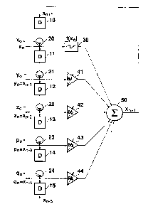
Fig. 3 illustrates a functional configuration o-f a chaot-
ic signal generator designed to find a solution Xn - {xn, yn,
zn, pn, qn, ...}T (Expression 13) of the recurrence equation
expressed as E~pression 3, or Expressions 4 through 8, or
Expression 10, or Expression 14.
The functional configuration comprises multiple delay
elements 10, 11, 12, 13, 14,..., initializing elements 20,
21, 22, 23, 24,..., each intervening between the delay ele-
ments, a nonlinear function element 30 receiving an output
from the initializing element 20, coefficient elements 41, 42
43, 44, ..., respectively, for multiplying outputs from the
remaining initializing elements 21, 22, 23, 24,...by coeffi-
cients al, a2, a3 a4, ..., respectively, an adding elemen-t 50
for summing up outputs from the nonlinear function element 30
and the coefficient elements 41, 42, 43, 44, .... . An output
of the adding element 50 is fed back to the ~orefront delay
element 10.
When the initial values XO = {xO, yO, zO, pO, qo, ...}T
are conferred throu~h the respective initializing elemen~s 20,
21, 22, 23, 24, respectively, the nonlinear function element
30 and the coefficient elements 41, 42, 43, 44,... produce
outputs f(xO), alyO, a2zO, a3pO, a4qO, ..., respectively,
whi~h are in turn summed up by the adding element 50 to obtain
an output xl. The output xl is fed back to the delay element
2~ 7:~
10 .
At any point in time, the nonlinear funation element 30
and the coefficient elements 41, 42, 43, 44, ...are allowed to
receive xn, yn = xn-1, zn = xn-2, pn = xn-3, qn = xn-4, re-
spectively, and produce outputs f(xn), alyn, a2zn, a3pn,
a4qn,..., respectively. As a result, the adding element 50
produces an output xn~1 expressed as Expression 4 which is in
turn fed back to the forefront delay element 10.
Naturally, the above-described operation is carried out
while incrementing n every one period ~ ~ of a clock
signal~ not shown in Fig. 3.
A sst of solutions Xn = {xn, yn, zn, pn, gn, ...}T which
may appear at the outputs of the delay elements 10, ll, 12,
13, 14, ..., respectively, are to be supplied externally in
terms of the outputs from the initializing elements 20, 21,
22, 23, 24,...each having the change-over switch bein~ con-
nected to the terminal TA.
In place of conferring the set of initial values X0 =
{xO, yo~ zo, po, qo,...}T through the corresponding initializ-
ing elements, there may be input xO, xl, x2, x3, x4, ...
(or, ..., x-4, x-3 x-2, x-1, xO) in sequence every one clock
period by way of the delay element 10 or the initializing
element 20. In this instance, the output of the adding ele-
ment 50 is not permitted to be fsd back to the delay element
lO until the input of all the initial values has been complet-
19
ed.
In Figs. 1 and 3, the coefficients a, al, a2, a3,
a4, ...of the coefficient elements 40, 41 42, 43, 44,....
respectively, are preferably externally changeable. Fur~
ther, a nonlinear function to be provided within the nonlinear
function element 30 is also preferably externally changeable
in configuration.
A more generalized recurrence equation having a plurality
of nonlinear functions will next be examined.
xn~1 = fO (xn) + fl(xn-1) + f2(xn-2) ~ f3(xn-3)
+ f4(xn-4) ~........................ ... Expression 15
Expression 15 can be modified as follows.
xn+1 = fO(xn) ~ yn ~ zn + pn ~ qn ~ ... Expression 16
yn = fl (xn-1) ... Expression 17
zn = f2 (xn-2) ... Expression 18
pn = f3 (xn-3) ... Expression 19
qn = f4 (xn-4) ... Expression 20
Fig. 4 illustrates a functional configuration of the
chaotic signal generator adapted to ind a solution xn, or a
set of solutions xn, xn-1, xn-2, xn-3, xn-4, or xn, yn, zn,
pn, qn,... with respect to the recurrence equations denoted by
Expressions 16 through 20.
The unctional configuration comprises multiple delay
elements lO, 11, 12, 13, 14,..., initializing elements 20, 21,
22, 23, 24,... each being interposed betwean ~he corresponding
- . ~
, :. .
2~7~
delay elements, nonlinear function elements 30, 31, 32, 33,
34, ...which recieve outputs Erom the corresponding initializ-
ing elements 20, 21, 22, 23, 24,..., and an adding element 50
which sums up outputs from the nonlinear function elements 30,
31, 32, 33, 34,.... An output xn+1 of the adding element 50
is fed back to the foremost delay element 10. The nonlinear
function elements 30, 31, 32, 33, 34, ... are provided with
nonlinear functions fO, fl, f2, f3, f4..., respectively.
Upon impartment of initial values xO, x-1, x-3, x-
4,....through the initializing elements 20, 21, 22, 23,
24,..., the nonlinear function elements 30, 31, 32, 33,
34,...produce outputs fO(xO), yO=fl(x-1), zO = f2(x-2~, pO =
f3(x-3), qO = f4 (x-4), ...which are in turn summed up with
the aid of the adding element 50 to obtain an output xl. The
output xl is then fed back to the delay element 10.
At any point in time, the nonlinear function elements 30,
31, 32, 33, 34,... recsive outputs xn, xn-1, xn-2, xn-3, xn-4,
respectively, and generate outputs fO(xn), yn = fl(xn-l), zn =
f2(xn-2), pn=f3(x-3), qn = f4 (xn-4), ...respectively. As a
result, the adding element 50 produces an output xn+1 repre-
sented by Expression 15 or 16 which is in turn fed back to the
delay element 10.
Naturally, the above-described operation is carried out
while incrementing n every one period ~t of the clock signal~
also not shown in Fig. 4.
21
- .... ,.,. , : , . ~ .. . ..
The outputs ~n, xn-1, xn-2, xn-3, xn-4,...which may
appear at the outputs of the delay elements 10, 11, 12, 13,
14,... are to be supplied externally in the orm of the out-
puts of the initializing elements 20, 21, 22, 23, 24,...whose
change-over switches are each connected to the respectlve
t~rminals TA.
As described earlier, the outputs fO(xn), yn = fl(xn-1),
zn = f2(xn-2), pn = f3(xn-3), qn = f4(xn-4) can be derived
from the nonlinear function elements 30, 31, 32, 33, 34,....
respectively.
In place of the initializing elements 21, 22, 23, 24,~..,
initial values yO = fl(x-1), zO = f2(x-2), pO = f3 (x-3), qO =
f4(x-4)... may be input through initializing elements 61r 62,
63, 64,..., respectively, to the output of the nonlinear
function elements 31, 32, 33, 34,...(and the corresponding
input of the adding element 50) as indicated by a chain line.
Also in Fig. 4, the nonlinear ~unctions to be set in the
nonlinear function elements`30, 31, 32, 33, 34,...are prefera-
bly changeable.
The configuration shown in Fig. 3 may be supposedly
dissolved into severaL units on the electronic circuit. Figs.
5 and 6 each illustrates a unit which is an elementary func-
tional constituent of the configuration shown in Fig. 3. A
circuit illustrated in Fig. 5 is called a linear delay unit
(hD). The linear delay unit (LD) includes a delay element li,
.- . ~ .
,: . - : . .: . .
:: .- . ~ . .
2 ~ $ ~
an initializing element 2i and a coefficien~ element 4i (i =
1, 2, 3, 4,...), the initializing elemsnt 2i being connected
to the output of the delay element li, and the coefficient
element 4i being connected to the output of the initializing
element 2i. The linear delay unit (LD) further includes an
input terminal through which an input xn-i+1 enters the delay
element li, an output terminal for supplying an output xn i of
the delay element li via the initializing element ~.i, an input
terminal for the entry of an initial value xO (or yO, zO, pO,
qO, ...), and a decorative output terminal for the departure
of an output ai.xn-i of the coefficient alement 4i.
A circuit shown in Fig. 6 is called a nonlinear delay
unit (ND). The nonlinear delay unit (ND) includes a delay
element li, an initializing element 2i, and a nonlinear func-
tion element 3i (i = O, 1, 2, 3, 4,...), the initializing
element 2i being connected to the output of the delay element
li, and the nonlinear element 3i being connected to the output
o the initializing element 2i. The nonlinear unit (ND)
further includes an input terminal for the entry of an input
xn-i+1 to the delay element li, an output terminal for the
departure of an output xn-i of the delay element li by way of
the i~itializing element 2i, a decoxative output terminal for
the departure of an output i(xn-i) of the nonlinear function
element 3i, and an input terminal for the entry of an initial
valua xO (or x-1, x-2, x-3, x-4,... ). ~;
2~7~ ~
If necessary, an initializin~ element 6i (i~ 1, 2, 3,
4,..) as indicated by a chain line in addition to an input
terminal for receiving an initial value ~ 0) may be provid-
ed on the side of the output of the nonlinear unction element
3i.
The output of one nonlinear delay unit (ND) is cascaded
to the inputs of a plurality linear delay units (LD), and the
terminals for the outputs fi(xn-i) and ai.xn-i of the units
(ND) and (LD) are connscted to the input of -the adding element
50. Finally, the output of the adding element 50 is fed back
to the nonlinear delay unit (ND) for establishing the circuit
shown in Fig. 3.
Such a nonlinear delay unit (ND), a plurality of linear
delay units (LD), and an adding unit 50A including the adding
element 50 can be integrated on one chip. Fig. 7 schematical-
ly illustrates a chip layout of a thus integrated chaos de-
vice. This layout omits a wiring pattern for joining one unit
to another. The adding unit 50A may comprise an operational
amplifier and an input resistor array associated therewith.
~ n a similar manner, a plurality of nonlinear delay units
(ND) are arranged in a cascade, and the terminal for the
output fi~xn-i) of each unit (ND) is connected to the adding
element 50. Finally, the output of the adding element 50 is
fed back to the foremost nonlinear delay unit (ND), ~hereby
establishing the circuit as shown in Fig. 4.
24
~ . ; : ~ . ,
It is possible to integrate on one chip suoh a plur~llty
of nonlinear delay units (ND) and the adding unit 50A includ-
ing the adding element 50. Fig. 8 diagramatically illustrates
a chip layout of thus integrated chaos device. This layout
also leaves out a wiring pattern for coupling one unit to
another.
Generalized recurrence equations are expressed as fol-
lows.
xn+l = fl (xn, yn, zn, pn, qn, ...) ...Expression 21
yn+l = f2 (xn, yn, zn, pn, qn, ...) ...Expression 22
zn+l = f3 (xn, yn, zn, pn, qn, ...) ...Expression 23
pn~l = f4 (xn, yn, zn, pn, qn, ...) ...Expression 24
qn~l = fS (xn, yn, zn, pn, qn, ...) ...Expression 25
fl, f2, f3, f4, f5,... denote multivariate nonlinear
functions.
Fig. 9 illustrates a functional configuration of the
chaotic signal generator which produces a series of solutions
of the recurrence eguations represented by Expxessions 21
through 25. Expressions 21 through 25 are associated in
tandem with delay elements 11 through 15, initializing ele-
ments 21 through 25, and multivariate nonlinear function
elaments 71 through 75, respectively. The multivariate non-
linear function elements 71 through 75 are to be supplied with
outputs from all the initializing elements 21 through 25.
Outputs xn+l through qn~l of the multivariate nonlinear func-
"
`` 2~ L~
tion ~lements are supplied externally and are fed back to thecorresponding delay elements 11 through 15. Each of the
multivariate nonlinear function elements is not necessarily
fad with the outputs from all of the initializing elements. A
hop fi~ld model is a particular case using a weighted addition
and a threshold function as the multivariate nonlinear func-
tion.
The configuration shown in Fig. 9 may comprise a combina-
tion of generalized nonlinear delay units (GNLD) illustrated
in Fig. 10. Fig. ll depicts an IC chip layout of a chaos
device consisting of a plurality of generalized nonlinear
delay units (GNLD). A wiring pattern for joining one unit to
another is not shown in this layout.
An electronic circuit embodying the delay unit (LD) and
the nonlinear delay unit (ND) as discussed hereinbefore will
now ~e explained by way of example.
Fig. 12 depicts a circuit embodying the linear delay unit
(LD). For better understanding of the corresponding rela-
tionship of this figure with Fig. 5, input and output signals
are designated by the same reference numerals as shown in Fig.
5.
The delay elements comprise a couple of capacitors C1 and
C2, and a couple of change-over switches SW1 and SW~. The
change-over switches SW1 and SW2 are controllably changed over
with the cloc~ signal~ as shown in Fig. 13. The delay time
2~
: . ~ . :. :
:~
. ~ . : : .~ ::, :
~ t corresponds to one period of the clock signal~. The
coefficient element comprises an operational amplifier A11
including a feedback resistor Rf. A coefficient ai is change-
able by a value of the resistor Rf. The initializing element
comprises a switch SW3.
When the change-over switches SW1 and SW2 are connected
to the terminals T2 and T1, respectively, and the switch SW3
is turned on, an initial value xO is allowed to be input. The
input capacitor C1 is loaded under a voltage in accordance
with a voltage signal representing the initial value xO. The
voltage at the capacitor C1 is multiplied by -ai with the aid
of an inverting amplifier A11 for the storage within the
output capacitor C2.
Next, upon the connection of the change-over switches SW1
and SW2 with the terminals Tl and T2, respectively, as shown,
the input capacitor C1 is charged under a voltage correspond-
ing to the input xn-i+l. While on the contrary, the voltage
at the output capacitor C2 is output in the form of the output
ai.xn-i by way of an inverting amplifier A12.
When the change-over switches SW1 and SW2 are again
connected to the terminals T2 and T1, respectively, the volt-
age at the input capacitor C1 is multiplied by -ai to be
stored within the output capacitor C2. In this manner, an
input is fed in while an output is supplied to the outside
every infinitesimal time ~t.
27
' ; . ! . i
. ` .' ~' '' ' ;
' ' . ' . ~ . ' ' ' ' ` '
' '' ''`i ~ ., i, i
2~7:~
- As described above, the change-over switches SWl and SW2
and the switch SW3 may be realized by a semiconductor switch-
ing circuit. The switch SW3 may be manually directly or
indirectly operated or controlled. A buffer circuit may be
appropriately provided within such a linear delay unit or
between such linear delay units.
Fig. 14 illustrates, by way of example, another configu-
ration embodying the linear delay unit (LD). In this figure
and figures which will be referred to later, also, the switch-
es or capacitors are designated by the same reference numerals
SWl, SW2,...and Cl, C2,... as in Fig. 12, which are merely
repeatedly used for the convenience of avoiding complexity.
It is to be appreciated that the reference numerals used in
one of the figures are lndependent of those used in another.
A circuit shown in Fig. 14 comprises a plurality of
(three in the figure) capacitors C1, C2, C3 and a plurality of
swi~ches SW1 to SW8. The switches SW1 to SW5 are controlled
by a clock signal ~1, while the switches SW6 to SW8 are con-
trolled by a clock signal ~2. The clock signal ~1 has a
phase opposite to that of the clock signal ~2 as is clear from
Fig~ 15.
When the switches SW1 to SW5 are turned on under the
control of the clock signal ~1, the switches SW6 to SW8 remain
off. Fig. 16A illustrates a circuit to be established at that
time. ~he three capacitors Cl, C~, C3 being connected with
28
.- .. :: ~ . .. . : - ~
. - : : :
. : , . - ~: . . . . .
.~. . . ::: :: : : ::, . :
one another in parallel are charged under the same voltage in
compliance with an input voltage signal vin.
Thereafter, when the switches SW6 to SW8 are alosed b~
the clock signal ~2, the switches SW1 to SW5 are caused to be
open. Fig. 16B illustrates a circuit to be established at
that time. The three capacitors C1, C2 and C3 are connected
in series. Consequently, the resultant output signal vout can
be represented as 3vin. As a result, the circuit shown in
Fig. 14 presents an output three times as great as the input
signal vin with a time delay of infinitesimal time ~t.
In the following description, the input signal xn-i~l and
the output signal xn-i are replaced by the input signal vin
and the output signal vout, respectively, for the simplifica-
tion of notation in the same manner as shown in Flg. 16.
As with Fig. 14, a selective on-off control of the
switches SW2 to SW7 enables the coefficient ai of the coeffi-
cient element to be changed.
In order to charge the capacitors C1 to C3, the switches
SWl to SW5 are turned on, whereas the switches SW6 to SW8
are turned of as shown in Fig. 16~.
Next, to derive the output vout from electric charge
accumulated in the capacitors C1 to C3, the switches SW6 and
SW8 are turned on, while the switch SW7 is left off. Further,
the switches SW1, SW2 and SW4 are turned off, while the
29
. . ,
2~3~
switches SW3 and SW5 are kept on. Thus, the capacitors C2 and
C3 remain connected in parallel to present the output vout of
2vin. Depending on the operation of the switchss SW1 to SW8,
there can be obtained an output of vout = vin.
Ins~ead of the foregoing, either or both of the switches
SW2 and SW3 may be left on at all times, whereby eleGtric
charge stored in ths capacitors C1 and C2 is permitted to be
discharged when a corresponding one or both of the switches
SW6 and SW7 is turned on, thus enabling the output voltage
vout to be 2vin or vin.
In this manner, appropriate change of the on-off con-
trol of the switches SW1 to SW8 makes it possible to obtain a
desired coefficient ai. Furthermore, the increase in number
of the capacitors to be connected may lead to an enhanced
freedom to choose a value of the coefficient. More specifical-
ly, a multiplicity of capacitors and switches arranged in
advance on an IC substrate may b~ configured as a mask pro-
grammable or field programmable logic array so as to obtain a
desired coefficient ai. This will also apply to other con-
crete circuits using a multiplicity of capacitors described
later.
Initializing elements, although not shown in Fig. 14
for the purpose of avoiding complexity, may be ad~ed under an
aspect shown in Fig. 12. The initializing element may con-
sist in general of a switch and a capacitor for holding a
. . . :~ ~;- , - : ... - . :
-
voltage representing an initial value which is input when the
switch is turned on. The same will apply to the other embodi-
ment described later.
The circuit shown in Fig. 14 includes a plurality o
capacitors connected in parallel and charged under an input
voltage. ~y connecting these capacitors in series, there can
be o~tained an output (ai > 1) having a voltage higher than
the input voltage.
On the contrary, by connecting in parallel a plurality of
capacitors which have been serially connected and charged
under an input voltage, there can be obtained an output (ai
<1) having a voltage,lower than the input voltage. Fig. 17
illustrates an exemplary configuration thereof.
The circuit shown in Fig. 17 comprises a plural,ity of
(three in the figure) capacitors C1, C2 and C3 and a plurality
of switches SWl to SW8. The switches SWl to SW3 are con-
trolled by a clock signal ~1, while the switch SW4 to SW8 are
controlled by a clock signal ~2. The clock signals ~1 and ',
~2 are the same as those shown in Fig. 15.
When the switches SWl to SW3 are turned on by the clock
slgnal ~1, the switches SW4 to SWB remain off. Fig. 18A
illustrates a circuit to be established at this time. Three
capacitors Cl, C2 and C3 are connected in series and charged
in compliance with the input voltage signal vin.
Afterwards, when the switches SW4 to SW8 are closed by
31
2~8~7~ ~
the clock signal ~2, the switches SWl to SW3 become open.
Fig. 18B illustrates the thus established circuit in which the
three capacitors C1, C2 and C3 are connected in parallel.
Therefore, if Cl = C2 = C3, then the output signal vout is
vin/3. In other words, the circui-t shown in Fig. 17 is al-
lowed to produce an output 1/3 times the input signal vin with
a delay of infinitesimal time ~t.
Depending on the manner of setting values of the capaci-
tors Cl, C2 and C3, there can be obtained an arbitrary coeffi-
cient ai (ai< 1).
For example, let C1 = 4C, C2 = 2C, C3 = C, where C means
a unit capacitance. In Fig. 18A, the capaci-tors C1, C2 and C3
each have an equally accumulated electric charge. ~et the
equally accumulated electric charge be Q, and let the volt-
age at both ends of each of the capacitors C1, C2, and C3 be
vl, v2, and v3, respectively. Then, the following expressions
are established with respect to the capaci~ors Cl, C2 and C3.
Q = 4Cvl ... Expression 26
Q = 2Cv2 ... Expression 27
Q = Cv3 ... Expression 28
On the other hand,
vin = vl + v2 ~ v3 ~.. Expression 29
Hence,
Q/C = t4/7) vin ... Expression 30
While on the contrary, in Fig. 18, the electric charge of
, ~ : ;: .
- 2 0 3 9 ~
3Q is redistributed among the three capac~tors C1, C2 and C3.
The amount of the electric charge to be stored within the
capacitors C1, C2 and C3 is 4Cvout, 2Cvout and Cvout, respec-
tively, and accordingly, the following expression is obtained.
4Cvout + 2Cvout ~ Cvout = 7Cvout = 3Q ...Expression 31
Expressions 30 and 31 lead to
vout = (3/7) (Q/C) = (3/7) (4/7) vin
= (12/49) vin ...Expression 32
It is to be noted also in Fig. 17 that a selective on-off
control of the switches SW2 to SW7 ensures an arbitrary change
in the coefficient ai of the coefficient element.
Fig. 19 illustrates a still further embodiment, in which
any one of, or two o, or all of the capacitors Cl, C2 and C3
are loaded under the input voltage vin, and then the electric
charge accumulatad in the loaded capacitor(s) is redis-tributed
among the three capacitors to derive an output voltaga vout
therefrom.
For instance, the switch SW1 is only turned on with the
aid of the clock signal ~1. Other switches SW2 to SW6 are
kept off. As a result, the capacitor C1 is charged under the
input voltage vin. Thereafter, the clock signal ~2 is used
to turn on the switches SW4 to SW6. The other switches SW1 to
SW3 are left off. Then, the electric charge accumulated in
the capacitor C1 is distributed among the o~hPr capacitors C2
and C3, and the output vout of a voltage depending on the
20~7~ ~
configuration of these capacitors is produced. Hence, vout <
vin, that is, ai < 1 is established.
In lieu of clos~ng the switch SWl, the switch SW2 may be
closed with ths aid of the clock signal ~1, thereby allowing
capacitor C2 to be charged. Alternately, the switch SW3 may
be closed so as to allow the capacitor C3 to be chargedj or
two of the switches SWl to SW3 may be closed to allow the
charge of the corresponding two capacitors.
Fig. 20 illustrates an exemplification of the nonlinear
delay unit (ND). For better understanding of the correspond-
ency to Fig. 6, the input and output signals are designated by
the same reference numerals as those used in Fig. 6. An
embodiment of the nonlinear function element 3i will be dis-
cussed later.
Fig. 21 depicts an embodiment of the nonlinear delay unit
(ND) comprising capacitors Cl to C4, diodes Dl to D3, and
switches SW1 to SW5. For simplification, assume C1 = C2 = C3
= C4.
Fig. 22A represents a charging state in which by virtue
o a clock signal~ the switch SW1 is on, the change-ovar
switches SW2 to SW4 are brought into contact with correspond-
ing terminals T1, and the switch SW5 is off. Let vD ba a
forward drop voltage of the diodes D1 to D3.
If the input voltage vin < VD, then only the capacitor C1
is allowed to be charged. If VD < Vin < 2VD, then the
34
- : : .. . - . .
~ . ~....... . . .
2~7~ ~
capacitors Cl and C2 are allowed to be charged. If 2vD < vin
< 3vD, then the capacitors C1, C2 and C3 are charged. I~ 3vD
< vin, then all of the capacitors Cl to C4 are sub~ected to a
charge. In this manner, the number of capacitors to be
charged depends on the magnitude of the input voltage vin.
- Moreover, Fig. 22B represents a state of producing an
output voltage in which by virtue of the clock signal~ the
switch SW1 is off, the change~over switches SW2 t~ SW4 are
brought into contact with corresponding terminals T2, and the
switch SW5 is on. All of the capacitors Cl to C4 are con-
nected in parallel, so that the electric charge in the first
charged capacitor is distributed among all the remaining
capacitors.
The number of capacitors to be charged and the quantity
of electric charge depend on the magnitude of the input volt-
age vin. Hence, input voltage vin/ output voltage vout char- `
acteristic can be represented as Fig. 23. This characteris-
tic is a nonlinear one. More specifically, in the case of the
circuit shown in Fig. 21, the output voltage vout which is
obtained by converting the input voltage vin through the
nonlinear characteristic shown in Fig. 23 is permitted to ~e
output with a delay of infinitesimal period ~t with respect
to the input point of the input voltage vin.
Fig. 24 illustrates, by way of example, an electronlc
circuit embodying the nonlinear function element 3i. This
, ............. . . . , ~ . ~ .
2~97.~
circuit includes a nonreversing operational amplifier A2
having a feedback adjustable resistor Rf. An input voltage
vin is supplied through input resistors to positive and
negative input terminals of the amplifier A2. With respect to
the negative input terminal of the amplifier A2, a couple of
diodes Dl and D2 (although these diodes are also designated by
the same reference numerals as those shown in Fig. 21, there
is no corresponding relationship between them) are connected
through the input resister in parallel and with opposite
polarity to each other. A voltage of -E1 is applied through
the adjustable resistor R1 to the anode of one diode Dl, whila
a voltage of ~E2 is applied through the adjustable resistor R2
to the cathode of the other diode D2. The output voltage vout
is derived from the output terminal of the amplifier A2.
Now, providing the forward drop voltage vD of the diode
is ignored and the input voltage vin satisfies
(R3 + R4) (R5 + R6)
vin > E2 ~..Expression 33
R4R5 -~ R4R6 + R3R6
then, the only diode D2 is conductive, and the circuit shown
in Fig. 24 can be represented in the form of Fiy. 26A. This
clrcult exhibits a positive amplification degree which can be
ad~usted by at least any one of the resistors R2 and Rf.
Providing the input voltage vin satisfies
36
..
, . . :: .: :
. ,.. , . . :- . .
. - . ~ .: : . : ~ : :
2 ~
(R3 + R4) (R5 + R6) (R3 + R4) (R5 -~ R6)
- - - El < vin < E2
R4R5 ~ R4R6 + R3R6 R4R5 ~ R4R6 ~ R3~6
...Expression 34
then, the diodes Dl and D2 are both nonconductive, and the
circuit shown ir. Fig. 24 can be represented in the form of
Fig. ~6B. Through an appropriate choice of the feedback
resistor Rf of the amplifier A2, a negative amplification
degree can be imparted to the circuit.
Providlng the input voltage vin satisfies
(R3 + R4) (R5 ~ R6)
vin < - - El ...Expression 35
R4R5 + R4R6 + R3R6
then, the diode Dl is only conductive, and the circuit shown
in Fig. 26C is established. This circuit also exhibits a
positive amplification degree which is capable of being ad-
justed by at least any one of the resistors Rl and R~.
Therefore, the input/output characteristic o~ the circuit
shown in Fig. 24 presents a nonlinearity as shown in Fig. 25.
The various kinds o electronic circuits described above
are all designed to function in voltage mode.
The following is a description of embodiments of a linear
delay unit (LD) ànd a nonlinear delay uni-t ~ND) which are
operated in current mode.
Fig. 27 illustrates, by way of example, a circuit embody-
.- :. . : : : .. ~; :
.,. . , , , :,,
2~$~
ing the linear delay unit (LD) which works in current mode.
The circuit comprises a couple of switched current mirrors.
The switched current mirror resting on the input side includes
nMOS(n-channel metal oxide semiconductor)FET(ield-effeGt
transistor~'s Ql and Q2 constituting a current mirror, and an
nMOSFET Q5 serving as a switching element and connected be~
tween gates of the FET's Ql and Q2. An input signal is
imparted to the FETQl in the form of a current Ii. The
switched current mirror lying on the output side includes
pMOS(p-channel metal oxide semiconductor)FET's Q3 and Q4
constituting a current mirror, and a pMOSFET Q6 acting as a
switching element and connected between gates of tha FET's Q3
and Q4. An output signal is derived from the FETQ4 in the
form of current I0. The FET's Q5 and Q6 each functioning as
the switching element are controlled by a clock signal~
(refer to Fig. 13).
When the clock signal~ is high, the FET's Q5 and Q6 are
on and off, respectively. With the FET Q5 on, the current
mirror on the input side is operated. Thus, when the FET Q1
receives an input current Ii, corresponding current I2 is
allowed to flow into the FET Q2.
Let a ratio of channel width to channel length (referred
to as W/L ratio hereinbelow) of the FET Q1 and a W/L ratio of
the FET Q2 be Wl/L1 and W2/L2, respec-tively, the current I2
can be written as
2~3~7~
I2 = [ (W2 / L2) / (Wl / Ll) ] Ii ...Expression 36
At that time, a parasitic capacitor CGDI located between
the gate and the drain of the FET Q2 stores an eleatric charge
corresponding to the current I2 and representing a voltage
equal to the gate voltage. The current I2 is allowed to flow
into the FET Q3 to cause a voltage drop corresponding to the
current I2 betwePn the gate and the drain of the FET Q3.
Thereafter, when the clock signal becomes low, the FET's
Q5 and Q6 become off and on, respectively. Therefore, the
current mirror is actuated. That is, a voltage arising from
the electric charge accumulated within the capacitor CGD1
continues to force the current I2 to flow into the FET's Q2
and Q3, while a capacitor CGD2 is charged through the ener-
gized FET Q6 up to the voltage equal to the voltage drop
between the gate and drain of the FET Q3 which may appear at
that time. As a result, the FET Q4 situated on the output
side receives corresponding output current IU. Let a W/L
ratio of the FET Q3 and a W/L ratio of the FET Q4 be W3/L3 and
W4/L4, respectively, the output current IO can be written as
IO a ~ ( W4 / L4) ~ (W3 / L3) ] I2
- ~ (W4 / L4) / (W3 J L3) ].
[ (W2 / L2) J (Wl / Ll)] Ii
= ai . Ii ... Expression 37
ai = [(W4 / L4) / (W3 / L3)].
[(W2 / L2) / (W1 / Ll)] ... Expression 38
39
. :
2~$~
In consequence, the output current IO has a current value
ai times as great as the input current Ii, and is output with
a delay of infinitesimal time at with respeGt to the lnput
point of the input current Ii. Preferably, a coefficient ai
is adjusted through the ratios W4/L4 and Wl/Ll.
Such a current mode circuit is suitable for integration
because of its wired sum and fewer number of components. For
example, comparisons with the linear delay unit in voltage
mode shown in Fig. 12 will be made hereinbalow.
The linear delay unit (LD) in voltage mode shown in Fig.
12 requires three resistors, which may result in a greater
area being required to accommodate them. In order to realize
the operational amplifiers and switches involved therein using
the transistors, there may be needed 11 to 20 transistors. It
also requires at least two capacitors.
While on the contrary, the linear delay unit (LD) in
current mode shown in Fig. 27 requires no resistors. It does
not need any capacitors, either, because it makes use of the
gate capacitance of the F~T. As is apparent from Fig. 27,
only six transistors are required to be provided therein.
Referring next to Fig. 28, description will be given of a
current mode circuit embodying the nonlinear delay unit (ND).
In Fig. 28, identical reference numerals are imparted to
the same elements as those shown in Fig. 27.
By comparison with the circuit in Fig. 27, the circuit in
2 ~
Fig. 28 includes a nonlinear function element SC In place o~
-the FET Ql lying on the input side. This nonlinear function
element SC exhibits a nonlinear current/voltage characteris-
tic, which may be realized by, for example, a thyristor. It
may be externally provided on the IC, or alternatively may be
embedded within the IC chip.
Since the capacitor CGDl stores an electric charge repre-
senting a voltage subjected to a nonlinear conversion with
respect to the input current Ii, the circuit shown in Fig. 28
produces a nonlinearly converted output current IO after the
lapse of time ~t.
Final description will be made of an applied example of
the chaos device discussed above.
A simplest configuration shown in Fig. 1 is implemented
by computer software, a simulation result based on which will
be explained.
Expressions 1 and 2 are rewritten as follows.
xn+l = f (xn) + a2yn ...Expression 39
yn+l - xn ...Expression 40
A nonlinear function f(xn) is expressed in the form
x ~ cosx2
f (xn) = alx + Expression 41
1 + X2
where al and a2 denote a constant (a parameter).
The nonlinear function f(x) represented by Expression ~1
2 ~ 7 :~ ~
describes a curve shown in Fig. 29. Lst al = 0.300.
Figs. 30 through 34 plot on XY coordinates a set pf
points designating (xn, yn) obtained from Expression~ 39
through 41. With n = 1 to 2000Q, there appear 20001 points
thereon including the initial value (xO, yO).
Fig. 30 illustrates a pattern obtained under the condi-
tions of initial values xO = 0.000, yO = 0.000; and parame-
ters al = 0.300, a2 = -1.000.
Fig. 31 depicts a pattern obtained by changing the ini-
tial values into xO = 5.000 and yO = 5.000 with the parameters
fixed (al = 0.300, a2 = -1.000). It will be seen from these
figures that the change of the initial values may bring about
a substantial change in the pattern consisting of a set of
points.
Fig. 32 represents a case where the parameters (al =
0.300, a2 = -1.000) remain fixed and the initial values have
been further changed into xO = 10.000 and yO = 10.000. The
pattern consisting of a set of points undergoes a further
transformation.
Fig. 33 shows a pattern obtained in the case where the
initial values are the same as those in Fig. 30 (xO = 0.000,
yO = 0.000) and one parameter has been slightly changed into
al = 0.290 (a2 = -1.000 remains fixed). Unlike the case in
Fig. 30, the pattern is substan-tially confined within the
range -1 < x, y < +2. It will be appreciated from the figure
.
42
- . . . .
2~7~
that a slight change of the parameters may cause a great
change in the pattern.
Fig. 34 illustrates a case where one parameter has been
further changed into al = 1.000, and the initial values (xO -
0.000, yO = 0.000) and the other parameter ta2 = -1.000) are
unchanged. The pattern undergoes a complete transformation.
Conceivable is a variant two-dimensionally displaying
such set of points (xn, yn). A display device may, for exam-
ple, be a CRT display unit, a plasma display, a liquid crys-
tal display, or a device including point sources of light
arranged in a matrix manner.
Manners of displaying are as follows.
1) Display of Pattern Formation Process
Points represented by (xn, yn) which will be obtained
while incrementing n every fixed interval of time are dis-
played in sequence. The points which have already been dis-
played may be deleted or may be left as they are.
This display reveals the state of formation of the pat-
tern with a lapse of time, or a locus o the points.
2) Display of Static Pattern
A set of coordinates representing a predetermined number
of (e.g., 20001 as described above) points is in advance
found, and all of such points are displayed at one time. The
patterns as shown in Figs. 30 to 34 will appear.
3) Display of Dynamic Pattern
43
.
-
With respect to the display of static pattern shown in
2), n is further incremented -to find a new point. The ob-
tained point is additionally displayed whereas the display o-
~the oldest point is deleted. Although the number o~ the
points being presently displayed are always unchanged, its
display pattern varies with a lapse of time.
4) To causa at least one of initial values and parameters to
be changed.
This method may apply to all of 1) through 3) described
above.
With respect to the manner of display stated in 2) in
particular, the display pattern is sub~ected to an abrupt
changej for example, from Fig. 30 pattern to Fig. 31 pattern,
or from Fig. 32 pattern to Fig. 33 pattern, etc.
Such display will be effective in a background display of
advertisement. The above-described change in pattern and
locus of the points are quite random and impossible to pre-
dict. Nevertheless, without causing any unplaasant feeling,
as noise does, it is interesting and attractive to look at.
Although the above description has been made of the case
where the dynamics of the system is expressed as difference
equations (e.g., Expression 1), the same will apply to the
case where it is expressed as differential equations in the
form
dx / dt = f(x) ~ ay ..~Expression 42
44
2~$~7 ~
dy / dt = x ...Expression 43
In this case, the delay element may be replaced with an
inteyral element. In the present invention, the delay ele-
ment, delay means, and delay circuit involve an integral
element, integral means, and integrating circuit, respective-
ly .
.
.
.: . : , .: ::