Note : Les descriptions sont présentées dans la langue officielle dans laquelle elles ont été soumises.
2090731
TITLE OF ~ INVE~TION
Moire cancel clrcuit
FIEL~ OF 1~ lNVk~1 tON AND R~ATE~ ART STATEMENT
1. F'IELD OF TH~: INVE'NTION
The pre~ent invention rel~tes to a molre cancel
circult for reducing the vertical moire phenomenon on a
screen of a raster-xcanning type dlsplay monltor ln whlch
a cathode ray tube ix u~ed.
2. DESCRIPTION OF T~E RELATED A~T --
I~ recent yesr~, with the ~p~ead o~ personalcomputers etc.. there have ari~en variou~ re~ests for a
dl~pl~ monitor ~or displaying dat~. F~r ex~mple, ~rlou~
di~ferent dot-nu~bers are needed ~or the horizon~al and
vertical dlrectlon~ of the di~play monltor, and various
di~play sizes are needed for the display monltor.
Furthe~more, lt 18 required ~or one dlspl~y mo~i~or th~
di~p~ay mode can be selected from among plural mode~ of
the dot-number and the di~play si~e.
A conventional vertical deflection circuit inputs a
vertical synchronizing signal to a vertical output circuit.
An output of the vertical output circuit is supplied to a
horizontal deflection coil to which a sigmoid correction
capacitor is connected. A description of the operation in
the vertical deflection circuit is omitted because it is
not relevant to the subject matter of the
2090731
present invention described below.
In a TV set, the number of scAnn;ng lines, which
corresponds to a vertical display dot-number, is specified
in accordance with broadcast system stAn~Ards, and a
display size is fixed in accordance with a size of a CRT.
An aperture pitch on a shadow mask is designed with respect
to the vertical dot pitch so as not to generate the moire.
However, the display monitor for computers etc. has to be
able to display data with arbitrary display size and
arbitrary dot-number. This means that several values are
needed for each of the vertical display size (L), the
vertical dot number (N) and the vertical dot pitch (d),
which satisfy the predetermined relation ( L / N = d), on
condition that the vertical aperture pitch is fixed to a
specific value. Since it is difficult to produce various
values for the fixed vertical aperture pitch, the
conventional art is confined to the following methods of
compensation:
(1) when a pitch of the scanning line, hence the
vertical dot pitch is changed by changing a size of the
image display area, the degree of the moire generated by
cross interference between the vertical dot pitch and the
aperture pitch of the shadow mask can be reduced:
(2) when an aperture pitch in the vertical
direction of the shadow mask is changed, the degree of the
moire generated by the cross interference against the
2Q~90731
scanning line pitch can be reduced; and
(3) when the scanning line is made bold by blurring
the focus, the contrast (shading) of the moire pattern can
be softened, thereby making the moire pattern unnoticeable.
However, the above-mentioned conventional moire
reduction methods have the following shortcomings:
i) since a vertical length of the image display
area can be changed within only a small range, the degree
of moire reduction is very low;
ii) since production of the display monitors is
small in comparison to TV sets which are mass-produced, it
is too costly to change the aperture pitch of the shadow
mask;
iii) since a display monitor needs a resolution
very much higher than a TV set, it is quite undesirable to
blurr the focus;
iv) since a multi-scanning type display monitor
suitable for displaying many dot number and many modes of
display size is often needed, it gets more difficult to
overcome the above-mentioned shortcomings; and ~
v) since the display monitor is controlled by a
microcomputer more frequentiy in recent years, it has
become necessary to carry out all the controls with DC
voltages which are required by the microcomputer.
2 0 9 0 7 3 1
.
o~JECT ANn SUMM~RY OF T~E iN v~N~ ON
An obJect of the present invention is to o~er a
moire cancel circult which ls capable of redu~ln~ the
moire and mlnlmizing deterloratlon o~ resolution ln all
disPlay mode~ o~ the dlsplay monltor, and which can be
controlled with DC voltages that can be output
by ~ mlcrocomputer.
In order to achieve the above-mentloned o~ect,
the molre cancel ci~cult o~ the pre~ent lnventlon --
comprlses~
a ~lgmoid correctlon capacitor conn~cted to one
end of a ~ertical de~lection coll;
~ vertical output circuit for supplyin~ the
verti~al deflection coll wlth a vertlcal de~lectlon
curre~t in accordance with a vertical synchronizl~
~i~n~l, the vertlcal output clr~ult belng connected to the
other end of the deflectlon coil:
~ dlvlng clrcult for making a control slgnal
h~v~ng a perlod twice as lon~ ~s a ~erlod of the Yertlcal
synchronizing signal; ~nd
a vertical posltion shi~t circuit connected in
parallel with the si~mold corre~tion ~apacitor. ~he
vertical positlon shlft circuit comprislng a resi~tor and
switch~ng mean~ which is connected ln serles to the
resistor and is turned on and o~ ln response to the
control signal.
2090731
According to the above-mentioned moire cancel
circuit, the moire phenomenon can be made unnoticeable
anywhere on the screen, independent of an aperture pitch of
a shadow mask of a CRT, the display area of an image, and
the variety of display modes (dot number etc.) of a display
monitor. Moreover, deterioration of resolution can be
minimized, and the structure of the circuit is simple.
Therefore, in a multi-scanning type display monitor, the
development is significantly enhanced; the production cost
is very low; and quality of image is improved.
While the no~el ~eatures o~ the invention are
set ~orth partlcularly in the appended claims, the
lnventlon, both as to organlzation and content, will be
better u~derstood and appreci~ed, along wlth other
obJect~ and features thereo~, ~rom the following detailsd
deserlp~lon taken in conJunctlon wlth the drawin~.
~R~EF ~ESCRIPTION OF T~E DRAW~NGS
FIG.1 i~ a block dia~ram ~howing a prlnciple of
~irst e~bodlment.
FIG.2 is a tlme chart showing waveforms of
signals which are described in the description of
the pre~ent invention.
FIG . 3 ls a clr~uit diagram showing a concrete
circuit o~ the ~ir~t embodiment.
FIG.4 1~ a block dlagram showing a prlnciple of
209073 1
a second embodiment.
FIG. 5 is a circuit diagram showing a concrete
circuit of the second embodiment.
FIG. 6 is a circuit diagram showing a conventional
vertical deflec~ion circuit.
DESCRIPTION OF THE PR~KK~D EMBODINENTS
Hereafter, preferred embodiments of the present
invention are described with reference to the accompanying
drawings.
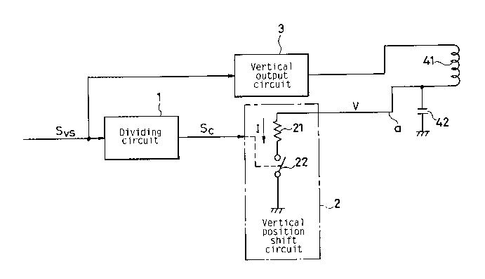
FIG. 1 is a block diagram showing a principle of operation
of a first embodiment. FIG. 2 is a time chart showing waveforms
of signals of the circuit shown in FIG. 1. In FIG. 1, a
vcrtical synchronizing slgna~ Sv~ (as shown in FIG.2) i~
input to a dividlng circuit 1. The di~id~ng circuit 1
make~ a con~rol signal Sc (as shown ln FIG.~ ~aving a
period tw~ce a~ lon~ as a period o~ the vertlcal
sy~chronizing ~ignal Svs and supplies the control ~ignal
Sc ~ a vertical posltion shi~t circuit ~. The vertical
positlon shift clrcui~ 2 consists of a reslstor 2~ and a
swltch 22. Al~o, the vert$c~1 ~ynchronlzlng si~nal Svs 18
input to a vertical output clrcuit 3, and the vertical
output circuit 3 supplies a vertical deflection coll 41
with a vertical deflect$on current. A sigmoid correction
capacitor 42 And the vertical position ~hlft circuit 2 are
connected to one ~nd of the vertical de~lection coil 41.
In the ~ositlon ~hift circuit 2, the switch 22 is
2090731
openedjclosed in response to the control signal Sc. When
the switch 22 is on (closed), a current flows through the
resistor 21. When the switch 22 is off (open), no current
flows through the resistor 21. As a result, a current I
shown in FIG. 2 flows in the resistor 21. This current I
is added to the vertical deflection current. Addition of
the current I causes a phenomenon whereby a display
position of an image shifts up or down at every vertical
period of the vertical synchronizing signal Svs. As a ~
result, a contrast (shading) of the moire is weakened,
thereby reducing the moire on the image. Since a screen of
the modern CRT is fairly flat rather than spherical,
deflection amount per a constant deflection current
decreases from the center of the screen toward edges of the
screen. Therefore, to evenly reduce the moire on the
image, the current added to the vertical deflection current
must be large at the center of the screen and small at the
edges of the screen.
In FIG.1, ~hen the switch 2~ i8 on, the rexistor
21 is connected ln parallel ~ith the sigmoid correctlon
capacitor 42. A capacltance of the sigmo~d correction
capacl tor 42 I s selected to have a predetermlned v~lue so
that a voltage V (as shown in FIG.2) having 8 parabola
wsve~orm, wh~eh corresponds to curvature of the xcreen o~
the CRT, can be generated across the ~lgmoid correction
capacitor 42 (at a point "a~). The current I added to the
20qO731
vertical deflection current is thus made parabolic in shape
periodically as shown in FIG. 2. As a result, the current
I is largest when an electron beam is scanning at the
center of the screen and gradually decreases toward the
upper and lower edges, thereby evenly reducing the vertical
moire of the overall image without any special modulation
circuit.
In the above-mentioned structure, a shift pitch of
the displaying position in the up or down direction is only
a minute value, less than an interval between the scanning
lines. A resistance of the resistor 21 is selected to
generate a proper shift pitch for obtaining the optimum
condition to reduce the moire.
FIG.3 is a clrcuit diagram showing a concrete
clrcuit o~ the first embodlment. The vertical po~i~lon
shi~t clrcuit 2 conslsts of resistors ~1, 24 ~nd an NPN
translstor 23 which corresponds to ~he swicth 22 of FIG.1.
The dividing circuit 1 conslsts of a re~ist~r 11 and a
flip-flop 12 as an example circuit in which the output
state is reversed in~accordance with a clock signal
(l.e., the vertical synchronlzlng sign~l). The vertical
syn~hronlzin~ slgnal Svs is also input to the vertical
output circuit 3, and a vertical output current is~ued
~rom the vertical output circuit 3 i8 supplied to the
vertical de~lection coll 41 to whlch the ~igmoid
correction capacitor 42 is connected.
Operatlon o~ the above-mentloned clrcult is
209U73 1
described with reference to FIGs. 2 and 3. An output Q of
the flip-flop 12 is reversed in state in response to the
clock signal. Since the clock signal is actually the
vertical synchronizing signal Svs as shown in FIG. 2, the
output Q of the flip-flop is alternately made high and low
at every vertical period to thereby act as the
control signal Sc shown ~n F~G.2. The output Q o~ the
flip-flop 12 ls supplled to the base o~ the NPN tran~istor
-23 by way o~ the re~istor 24. When the output Q o~ t~e-.
~llp-~lop 12 is high, the ~PN tran~stor 23 turns on, and
thereby the current ha~lng the parabola-shaped wave~orm
flows through the re~istor ~1 and the NPN transistor 23.
The current is thus added to the ~ertical de~lection
curren~. When the output Q of the flip-~lop 12 i8 low,
the NPN transi~tor 23 turns of~. There~ore, no current
flows through the re~lstor 21, and no current is added to
the vert~c~l de~lection current. Thus, the current I a8
~hown in FIG.2 is obtained. When the current I i~ added
to the v~rtical deflection current, a display position of
the image shifts on the screen. Therefore, the displaying
position of the image shifts relatively up and
do~n ln the vertical dlrectlon. The molre on the screen
is thereby reduced. Slnce the current added to the
vertical de~lection current ~Rrles ln response ~o a
reslstance o~ the reslstor 21, the molre can be made
unnoticeable ln any mode of the display monitor by
2090731
~ ,
selecting a proper resistance for the resistor 21.
When the display monitor of a 17-inch type CRT
which has a vertical screen length of 220 mm and an
aperture pitch of 0.28 mm, a vertical dot pitch for
handling 600 dots (i.e., 600 sc~nning lines) is 0.368
(=200/600) mm. In such a display monitor, the vertical
moire is canceled by an up or down shift of the scanning
line by only about 0.06 mm, whereas a diameter of an
electron beam spot is about 0.6 mm. Thus, since the shift
amount (=0.06 mm) is only ten percent of the diameter of
the electron beam spot, the vertical resolution is not
influenced much by the vertical shifts of the sc~nn;ng line.
The moire cancel circuit is not limited to the
circuit shown in FIG. 3. The essential point is that the
current, which is lower toward the vertical edges of the
screen than at the center of the screen, is periodically
added to the vertical deflection current, thereby shifting
a display position at a period that is twice as long as the
vertical period, to evenly reduce the moire over the entire
screen.
- FIG. 4 is a block diagram showing a principle of
another embodiment. This moire cancel circuit is
controllable with DC voltage. Corresponding parts and
components to the first embodiment are shown with the same
numerals and marks, and the description thereon made in
2090731
the ~irst embodiment i~ ~lmllarly applied. A dif~erence
of thls ~econd e~bodlment ~rom the ~lrst embodiment i~
provi~ion o~ a con~tan~ voltage gource 5 connected to the
vertical posltlon shl~t clrcuit 2. ~n output volta~e of
the con6tant volta~e ~ource 5 ls controllable wi~h DC
voltage. Herea~ter, operation o~ th~ moire cancel circuit
shown in FIG.4 18 de~cribed with reference to FIG.~.
The vertlcal synchronlzing signs~ SvS (FIG.2) i~
input ~o the dividing c~rcuit 1. The divldlng circuit 1--
ls~ue~ the control ~lgnal Sc (FIG.2) having a period twlce
~s long a~ the vertical period. In the vertical posltlon
shl~t circult 2, the switch 22 ls turned on or o~ in
response to the control signal Sc When the switch 22 is
on, a dif~erentLal voltage between the voltage at the
point "a" (F~.4) and an output ~oltage o~ the con~tant
voltage source S is applied between both ends of the
resistor 21, and a current flows in the resistor 21. When
the switch 22 is off, no current flows through the resistor
21. Thus, the current I (FIG. 2) is added to the vertical
deflection current. When the output voltage of the
constant voltage source 5 varies by varying the DC control
voltage, the voltage applied to the resistor 21 varies
during the on-time of the switch 22. Therefore, a DC
component of the current I (FIG. 2) added to the vertical
deflection current varies, thereby varying a shift amount
of the image. The current added to the vertical deflection
209073 1
current has a parabola-shaped waveform such that the
current is greater in the center of the screen and
gradually lessens toward the vertical edges of the screen.
The moire is thus reduced evenly over the entire screen. A
shift pitch of the display position in the up and down
directions is only a minute value of less than an interval
between the scanning lines. The output voltage
of the consta~t ~olta~e ~ource S is selected by
controlling the DC voltage to generate a proper sh~ft
pitch ~or obtaining the optlmum cond~tion to reduce the
molre.
FIG.5 is a circult dlagra~ showing a concrete
circult o~ the second embodiment. The vertical posltion
shi~t clrcuit 2 consist~ o~ resistors 21, Z4 and an NPN
transistor 23 which cor~esponds to the swl~ch 22 o~ FIG. 4 .
The dlviding c~rcuit 1 consists of a reslstor 11 and a
flip-flop 12. The fllp-flop 12 may ~e replaced by any
other known circuit in which the logic of output is reversed
in accordance w~th a clock signal ~l.e , the vertical
synchronizing si~nal). The constant voltage source 5
consists of a PNP transistor 51 whose base receives a DC
control voltage.
Oper~tion o~ the above-mentloned c~rcult is
described ~ith reference to Fl~s. 2 and ~. An outPut Q o~
the flip-flop 12 is reversed in state in response to
the cloc~ slgnal Since the clock signal ls actually the
2090731
vertical ~ynchronlzing signal Sv~ 8~ ~hown ln FIG.2, the
output Q of the flip-flop 12 is alternately made hl~h and
low at every vertlcal period as the control signal Sc
shown in FIG.2. The output Q o~ the ~lip-flop 12 1
~upplled to the ba~e o~ th~ NPN tr~nslstor 23 by way o~
`the resistor 24. The DC control voltage, which ~s applied
to the base of ~he PNP translstor S1, is selected to have
a value wlthln a ran~e ln which the NPN translstor 23 end
the PNP transi~tor 51 ~urn on when the output Q o~ the -
~llp-~lop 12 ls high. When the output Q o~ the ~lip-flop
1~ is high, the NP~ transl~or ~3 and the PNP transistor
51 turn on, and thereby the current having-the parabola
shaped ~aveform flows through the re~ixtor 21, the NPN
tran~lstor 23 and the PNP ~ranslstor ~. The current i8
thus added to the vertl~l de~lection ~urren~. When the
ou~put Q of the ~lip-~lop 12 lx low, the NPN translstor 23
turns o~f. There~ore, no curren~ ~low~ through the
resi~tor 21, and no current is added to the ~ertical
deflection current. Thus, the current I as ~hown in FIG.2
18 added to the vertlcal deflection current. When the
current I i~ added to the vertical deflection ~urrent, a
display position of the image shifts on the screen.
Therefore, the display position of the image shifts
relatively up or down in the vertical direction. The moire
on the screen is thereby reduced. The current added to the
vertical deflection current has a value dependent on a
2090731
`
resistance of the resistor 21 and a voltage appearing
between both ends of the resistor 21. Since the voltage
applied across the resistor 21 at the time when the output
Q of the flip-flop 12 is high depends on the DC control
voltage applied to the base of the PNP transistor 51, a
shift amount of the displaying position can be controlled
by the DC control voltage applied to the base of the PNP
transistor 51. The moire is thus made the least noticeable
by adjustment of the DC control voltage.
Althou~h th~ pre~ent lnvention ha~ ~een
described in term~ o~ the pre6ently preferred embodiments,
lt i~ to be under~tood that such disclosure ~s not to be
interpreted as limiting. Yarlous alteratlons and
modi~icatlon~ will no doubt become apparent to those
xkilled ln the art after having read t~e above disclosure.
Accordlngly, it i~ lntended that the appended c~alms be
lnterpreted a~ coverlng all alteratlon~ and modific~ti~ns
a~ ~all wl~hln the true splrlt and scope of the inventlon.