Note : Les descriptions sont présentées dans la langue officielle dans laquelle elles ont été soumises.
2o928a~o
AN INTEGRATED OPTICAL PACKAGE FOR COUPLING OPTICAL
FIBERS TO DEVICES WTTH ASYMMETRIC LIGHT BEAMS
Technical Field
The present invention relates to an integrated optical package including
an optical device with an asymmetric light mode) such as an elliptically-
shaped light
beam) and a lens for coupling the optical device to an optical fiber.
Background of the Invention
Future network systems may include long-haul optical communication
systems) interconnection technologies) two dimensional optical processing)
optical
computing and others. Semiconductor devices) such as lasers and
photodetectors,
are already an integral part of optical fiber communication systems. In
conjunction
with fibers, other semiconductor devices, such as modulators and optical
switches)
are also likely to be incorporated into the network systems.
Unfortunately, the utility of many such semiconductor devices is
hampered by their high fiber insertion loss which at least partially arises
from a
fundamental mismatch between a typical single-made fiber with a relatively
large
cylindrical core and, thus, a large circular modal input or (output) area) and
semiconductor devices having smaller modal output (or input) areas and
eccentricity
ratios greater than 1:1. Losses which arise in coupling light between optical
fibers
and these devices include those arising from the mismatch of the symmetry of
the
two modes (circular versus elliptical) as well as the mismatch of the average
modal
area.
In the past, symmetric hemispherically and hyperbolically shaped
microlenses have been fabricated on the end of an optical fiber by means of a
pulsed
laser beam. Set U.S. Patent No. 4,932,989, issued to H. M. Presby on June 12,
1990
and U.S. Patent No. 5,011,254 issued to C. A. Edwards and H. M. Presby on
April 30) 1991. Such microlenses afford relatively high coupling efficiency
for
devices) such as lasers) having a symmetric modal output) that is, for devices
whose
output beam profiles are circular or have ellipticity ratios close to 1:1
i.e.) where the
divergence of the output beam of the laser is the same or substantially the
same
along axes parallel and perpendicular to the junction plane of the laser. Use
of
hyperbolically shaped microlensed fibers has led to greater than 90 percent
coupling
efficiencies between optical fibers and devices having symmetric modal output.
However) the modal asymmetry exhibited by many semiconductor devices requires,
for good coupling efficiencies, asymmetric microlenses. There are many lasers
which have an elliptical beam structure with ellipticities from about 1:1.5
and even
higher) emanating from the laser facet. Use of symmetric microlenses for
coupling
2 - 2092840
elliptical light beams to fibers) led to significant decrease in the coupling
efficiencies.
For example) for such semiconductor devices as laser diodes with reasonable
modal
asymmetry) e.g. 1:2.5 to 1:3.5, fiber coupling efficiencies of up to 50
percent can be
obtained with symmetric microlenses, with 25 to 35 percent being more typical.
Since about half of the laser output is not utilized, the laser has to be run
at higher
currents to yield the same coupled power into fiber than a more efficient
coupling
scheme could give. Running the laser at higher currents results in greater
heat to be
dissipated. For example) when the coupling efficiency is at 50 percent, the
laser
thermal power dissipation is four times greattr than at 100 percent coupling
efficiency. This affects long-term stability and reliability of the lasers and
presents a
major obstacle in the development of uncooled laser diode technology. For
modulators and switches) where from a system design viewpoint an insertion
loss of
less than 0.5-1.0 dB is desired, the situation could be more serious. A
higher, e.g. 3
dB) insertion loss decreases signal to noise redo and increases system
complexity.
Attempts to increase coupling of fibers to elliptical beams with non-
symmetric lenses have been reported in the form of an externally mounted
cylindrical lens and a wedge-shaped fiber endface. See M. Saruwatari et al.
"Semiconductor Laser to Single-Mode Fiber Coupler," Applied tics Vol. 18,
No. 11, 1979) pages 1847-1856 and V. S. Shah et al. "Efficient Power Coupling
from
a 980nm, Broad Area Laser to a Single-Mode Fiber Using a Wedge-Shaped Fiber
Endface", J_. Lightwave Technology) Vol. 8, No. 9) 1990, pages 1313-1318. In
the
former case the coupling is effected by means of a lens and a cylindrical rod
placed
between a laser and an optical fiber) and in the latter case an end of the
fiber is
provided with an enlarged cylindrical portion terminating in a wedge-like
shape
which approximates a cylindrical lens. In the latter case) a coupling
efficiency of 47
percent was obtained. Clearly, what is required for optimum coupling between a
device with an elliptical light beam output (or input) area and an optical
fiber is a
lens which would transform the elliptical beam output of the device to match
the
circular single-mode filxr mode profile and vice versa
Summary of the Invention
This invention embodies an integrated optical package including an
optical Eomponent having an asymmetric modal output, and a lens integrated
with
the component for coupling to another optical component having a large modal
area.
The coupling is achieved by the use of a Polymeric Elongated Waveguide
Emulating
(PEWE) lens. In the exemplary embodiment the first optical component is a
modulator and the other optical component is an optical fiber. A facet of the
modulator is etched by reactive ion etching (ItIF) which allows integration of
the
2092s4o
-3-
PEWE lens on a common substrate. The lens is manufactured using a polymer
film on a dielectric cladding layer. The fabrication relies on the remelt and
reflow
properties of polymer films to provide a smooth adiabatic mode contraction
from a
circular (optical fiber) mode (~ 6~tm in diameter) to a semiconductor mode (~l
pm)
over a length of 250 pm. The PEWE lens permits coupling with an insertion loss
of 0.5 dB and 80 percent coupling efficiency, even though the lens is butt-
coupled to
a fiber without any external lens. The PEWE lens allows the realization of
better
than 80 percent direct fiber butt-coupling efficiencies to semiconductor
lasers,
photodetectors, optical modulators, switches and amplifiers with a
simultaneous
order of magnitude relaxation of the alignment tolerances typically needed for
the
coupling of semiconductor devices.
In accordance with one aspect of the present invention there is provided an
integrated optical package for coupling an optical device having an asymmetric
modal area and an optical fiber having a circular modal area, each to another,
said
package comprising: an optical device with an asymmetric modal area, and an
elongated wedge-like optical waveguide, said optical device and said optical
waveguide having a common substrate, an end portion of said optical waveguide
abutting a light emitting or light receiving facet of said device, and an
opposite end
portion of the optical waveguide being for optical coupling to an optical
fiber,
cross-section of that end of the optical waveguide which abuts said facet
matching
essentially the cross-section of the modal area of the device, and cross-
section of the
opposite end of the optical waveguide is designed to match essentially the
cross-section of the core of the optical fiber, said optical waveguide
comprises a
planar dielectric layer and a wedge-shaped lens of organic polymeric material
on
top of the dielectric layer, an upper surface of the dielectric layer and a
lower
surface of the lens are in alignment with a lower boundary of an active layer
of the
device.
In accordance with another aspect of the present invention there is provided
a method of fabricating an integrated optical package, said package comprising
an
optical device with an asymmetric modal area and an elongated lens for
coupling
the device to an optical component having large modal area relative to said
asymmetric modal area, which comprises: beginning with a substrate having a
compound semiconductor structure thereon comprising an active layer and a
bottom and a top cladding layers, etching a trench in said structure so as to
expose
~_ 2o92s4o
-3a-
a facet of a device on each side of the trench, said etching removing a
partial
thickness of the lower cladding layer and all of the other layers of the
structure
above said lower cladding layer while retaining those portions of said
structure
which are intended to be used as the optical device, forming in said trench
centrally
between two facets a diamond-shaped elevated form the length of which is equal
to
a half of the width of the trench between the facets, the thickness of the
diamond-
shaped form being equivalent to at least the diameter of the core of a fiber
to be
optically coupled to the device, coating the whole of the structure with a
thin layer
of a polymeric material in a thickness equivalent to the height of the active
layer in
said device, converting the profile of the combined polymeric material to a
profile
with a gentle slope between said center portion and said facet-adjoining
portion,
and removing an excess of thickness of said polymeric material adjacent each
facet
so as to reduce this thickness to that corresponding to the height of the
active layer
in said device.
Brief Description of the Drawings
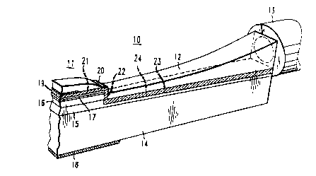
FIG. 1 is a perspective view of an integrated optical package showing
a microlens coupling an optical device to an optical fiber;
FIG. 2 is a perspective view of the microlens;
FIG. 3 is an enlarged schematic representation of a side view of a
portion of a compound semiconductor structure with a thin Si02 layer thereon
prior to formation of the microlens;
FIG. 4 is a top view of the structure of FIG. 3 with a diamond-like
shaped photoresist region;
FIG. 5 is a schematic representation of a side view in cross-section of
the structure of FIG. 4 with a continuous layer of photoresist over the whole
of the
upper area;
FIG. 6 is a schematic representation of the structure after the heating
and reflow of the photoresists shown in FIG. 5;
FIG. 7 is a schematic representation of an angle light exposure of an
area of the photoresist to remove unwanted photoresist from an end portion of
the
microlens adjoining the device;
FIG. 8 shows the microlens after removal of the unwanted
photoresist region and prior to separation of two adjoining lenses along the
center
line 27;
A
-3b- 20 9 28 4 0
FIG. 9 is a schematic representation of an intermediate step in the
formation of a polyimide microlens utilizing a reflown photoresist layer on
top of
the polymer layer; and
FIG. 10 is a schematic representation of the polyimide microlens
formed from the configuration of FIG. 9.
n
4 - 2092840
Detailed Dexriptton
This invention embodies an integrated optical package including a
semiconductor device having an elliptical mode output integrated with an
elongated
optical lens for coupling the device to an optical fiber with a circular mode
and vice
S versa. The package and process steps used in the fabrication of the package
are
described hereinbelow with reference to the drawings. For illustration
purposes)
various dimensions of the drawings are not drawn to scale.
Shown in FIG. 1 is a schematic perspective view representation of an
integrated optical coupling package) 10. Package 10 includes a compound
semiconductor device) 11) having an asymmetric modal output area) and a
coupling
optical lens, 12) formed integrally with the device and coupling an optical
mode
output (or input) of the device to an optical fiber 13. Lens 12 is of an
organic
polymeric material including photoresists and other polymers. For smooth
coupling
of optical energy from the device to a fiber and vice versa, lens 12 is in the
form of
an elongated wedge-like waveguide. This lens tray be referred to as a
Polymeric
Elongated Waveguide Emulating (PEWE) optical lens.
Typical semiconductor device 11 includes a semiconductor substrate,
14) a bottom cladding layer, 15, an active layer, 16, a top cladding layer 17,
and a
lower and a top electrodes) 18 and 19) respectively. The device may further
include
at least one other layer) such as a buffer layer positioned between the
substrate and
the bottom cladding layer, a highly doped contact layer positioned between the
top
cladding layer and the top electrode, a capping layer positioned on top of the
top
cladding or contact layer) and some other layers depending on the construction
of the
device, as is well-known in the art. Undoped or lightly doped transition
layers may
also be deposioed between the active layer and the cladding layers. The active
layer
may be a single layer) an alternating multilayer structure) or a structure
graded on
both sides of the active layer. Such layers are well-known in the art and may
vary
depending on the device.
A layer) 20) of an optically transparent dielectric material overlays a top
surface) 21) of the device, its light-emitting (or light-receiving) facet, 22)
and a
surface, 23, of the bottom cladding layer 15. Prior to deposition of the
dielectric
layer, the surface of facet 22 may be coated with a light-reflective coating.
Such
coatings as Agar or ZnS) are suitable for this purpose. Top surface 24 of
layer 20 is
aligned with lower boundary of active layer 16. Lens 12 rests on top surface
24 of
layer 20 and abuts that portion of layer 20 which is in contact with facet 22
of the
device. Since the lower surface of lens 12 is on surface 24 of layer 20, the
bottom of
the lens is also aligned with the bottom of active layer 16. To fit the lens
to the
20 9 28 4 0
- 5 -
cross-section of active region 16 and of the optical fiber) the lens is in the
form of a
truncated wedge. The narrower end of the wedge is aligned with and
approximates
the cross-sectional area of active region 16) while the wider end of the wedge
approximates the cross-section of at least the core of the optical fiber. The
face of
the lens at the narrow end has a rectangular-to-elliptical cross-section with
an
asymmetry ratio closely approximating that of the active region. The narrow
end of
the lens abuts facet 22 of device 11. The opposite face of the lens at the
wide end
has a square-to-circular or -elliptical cross-section which approximates at
least the
cross-section of the con of the optical fiber. A perspective view of lens 12
without
the dielectric layer and the substraoe is shown in FIG. 2. Optical fiber 13 is
shown
abutting the lens; however, it may be any other optical component with a
relatively
large modal area, relative to the modal area of the optical device 11.
A number of packages may be produced upon a single compound
semiconductor wafer, and then divided out, e.g. by cleaving into single or
duplex
packages or alternatively) into a parallel multiple of single or duplex
packages. A
duplex integrated package includes two semiconductor devices 11 integrally
produced on the substrate in a back-to-back fashion permitting insertion of an
optical
radiation from one optical fiber into one device via a related lens) transfer
of the
radiation from one device to another device, and then coupling of the
radiation from
said other device into another optical fiber via the related lens.
The production of the integrated optical package begins with a
semiconductor structure of the device upon a semiconductor wafer, formed by
depositing on the substrate a plurality of different layers by planar
technology. The
structure typically includes an active layer placed between a bottom and a top
cladding layers but may include other layers as is well-known in the art.
At least one flat trench is etched in the surface of the semiconductor
structure exposing vertical facets 22. The width of each trench between the
facets is
equal to twice the desired length of the lens. The distance between the
trenches is
selected to accommodate the length of two devices. Prior to forming the
lenses) the
etched facet may be coated with a thin antireflective coating) such as Agar or
ZnS.
Thereafter) the bottom of each trench, the facet and the upper surface of each
device)
are coated with a thin layer of an optically transparent dielectric material.
The trench
is of such depth and the dielectric material is of such thickness that, when
the
dielectric material is deposited on the bottom of the trench) the upper
surface of the
dielectric material in the trench is in alignment with the bottom boundary of
the
active layer in the structure. This assures alignment of the lower surface of
the lens
resting on the dielectric layer with the bottom boundary of the active layer.
_ 2os2$40
The lens is produced by depositing) on upper surface 24 of dielectric
layer 20 in the tench, a layer of an organic polymeric material, selected from
photoresists and other polymers, which is optically transmissive and has an
index of
refraction approximating that of the core of the optical fiber. The organic
polymeric
material after processing has in a longitudinal cross-section a truncated
wedge-likc
structure the upper surface of which slopes from the wide) optical fiber-
mating end
to the narrow) device-mating end. The thickness of the organic material is
small
relative to the length of the lens so that the upper surface of the lens
slopes gradually
from the wide end to the narrow end. In the preferred embodiment, the upper
surface
of the lens slopes from about 6-7 Etm at the wide) optical fiber end to about
1 ~m at
the device end over a length of about 250 ~tm. Thereafter) the organic
polymeric
material is timnxd laterally, e.g., by plasma etching) to remove any organic
polymeric material which is not needed for the transmission of the radiation
energy
from the device to the fiber and vice versa. The top view of the lens has the
shape of
a truncated triangle) with the broader base facing the fiber and with the
narrower base
facing the device. Because of the gentle slope of the wedge) them is little
possibility
of leakage of the radiation through the unprotected surfaces of the lens. To
reduce
even this possibility, exposed surfaces of the lens may be coated with a thin
layer of
dielectric material) such as Si02 with n = 1.47) which could block the
leakage.
Preferably, the coating material shall have an index of refraction which is
lower than
the material of the lens.
For illustration purposes, this invention is described with reference to an
optical modulator waveguide) having an elliptical light mode with a ratio of,
e.g. 1:3)
as the semiconductor device 11. This device is coupled to an optical fiber by
PEWS
lens 12 fabricated from a photoresist material having refractive index (n =
1.63)
approximating that of the core (n = 1.49 - 1.52) of the optical fiber. An
effective
fiber coupling efficiency of 80 percent with an order of magnitude relaxation
of the
typical alignment tolerances is obtainable with this arrangement.
Shown in FIG. 3 is an enlarged schematic representation of a section of
a compound semiconductor wafer acting as a semiconductor substrate with a
GaAs/AIGaAs device structure grown thereon by planar technology. In the
exemplary embodiment device 11 is a modulator having a structure including a
150
Etm thick GaAs substrate 14, a I .5 lun thick Al 0,4 Ga o.6 As bottom cladding
layer I 5)
a 50 period GaAs/AIGaAs active region 16, each period including a lOnm thick
GaAs layer and a lOnm thick Al 0,4 Gao,6 As layer) a 0.3 ~tm thick Al 0.4
Gaa.6 As
cladding layer 17) and a SOnm thick GaAs capping layer) 25. The light emission
takes place from the surface of a facet) 22, which is perpendicular to the
plane of the
-' - 2092840
drawing. The modulator is provided also with electrodes 18 and 19.
The modulator was prepared by depositing upon an about 500 ~m thick
GaAs wafer, to be used as substrate 14 of the modulator semiconductor, layers
15-17
and 25 in succession by planar technology deposition. The deposition may be
carried out by molecular beam epitaxy (MBE)) metal organic vapor phase epitaxy
(MOVPE)) also known as metal organic chemical vapor deposition (MOCVD)) or by
hydride vapor phase epitaxy (VPE). In the present embodiment the deposition
was
carried out by MBE. Thereafter, the coated wafer was patterned with a
photoresist
mask so as to delineate for trenches parallel to the face intended for light
emission.
The width of each trench) about 500 Vim, was selected to produce two lenses)
about
250 ~m long each) awanged back to back) each to another. The wafer was then
etched using a SiCl4 plasma to totally remove in delineated trench areas
layers 16,
17, and 25 and a small, about 0.5 ltm) thickness of the upper surface of
bottom
cladding layer 15. This small thickness was chosen to allow the etched surface
to be
about 0.5 ~m beneath the lower boundary of guiding or active region 16.
Vertical
walls were obtained by etching with plasma using 0.16 W/cm2 RF power and 5
mTorr working pressure. The etched side walls were as smooth as the edge
profile
of the photoresist mask used for defining the trenches. The wafer was then
thinned
down to 150 ltm) and 0.5 Itm thick Si02 layer 20 was deposited at 300°C
by plasma
enhanced chemical vapor deposition (PECVD) over the whole of the wafer, namely
over top surface 21 of capping layer 25, the surface of facet 22 and the
etched
surface 23 of bottom cladding layer 15. The Si02 layer serves as the bottom
cladding layer for the PEWE lens. Electrodes 18 and 19 may be deposited after
the
completion of the structure. Alternatively, the electrodes may be deposited
after the
deposition of Si02 layer 20. This would require formation of a window in layer
20
through which electrode 19 is then deposited.
A 7 ltm thick layer of AZ 4620~ photoresist was applied by spinning
over the Si02 coated surface of the wafer) and thereafter, elongated diamond-
like-
shaped photoresist areas 26 (FTG. 4) were patterned in the trenches centrally
between
the etched facets and with long apexes pointing in the direction of the
facets. In
Fig. 4, as well as in Fgs. 5-8) is shown a little more than one-half of the
trench
width and associated photoresists. The dash-and-dot line 27 represents the
center of
the trench and of photoresist ("diamond") area 26. Diamond 26 was from 10 to
50
~t,m wide in the central area and about 250 ~m long which is about one-half
the width
of the trenches between the devices. This allots half of the length of the
diamond
(about 125 Vim) to each of packages 10. Other dimensions of the diamond could
be
used as well so long as the width of the diamond exceeds the width of the area
to be
- a - 2092840
matched, e.g.,the diameter of the core of the optical fiber. The diamond was
then
post-baked at 120° C for 15 minutes to evaporate most of the solvent.
'Thereafter 1
~m thick layer of AZ 4110~ photoresist, 28) was spun on the wafer at rotation
speeds ranging from 3,000 to 5,000 rpm) preferably at 4000 rpm. The two
photoresists have similar solvent bases; however, the spinning of the AZ 4110~
at
higher rpms may partially smear out the diamond patterns. Spinning at lower
rpms
may lead to a thinner photoresist thickness. Alternatively) 1 Itm thick
photoresist
could be sprayed on the whole of the surface) including the diamond pattern.
In the
production of optical packages with other devices, the active layer may have
thickness and) thus) the height of the modal output area of the device) which
is more
or less than 1 Itm. In such cases, the rpms should be adjusted to obtain a
photoresist
thickness matching that of the active layer.
The photoresists used in the specific example are commercially
obtainable from Electronic Products Division of Hoechst Celanese Corporation.
The
AZ 4620~ contains 2-Ethoxyethyl Acetate ( 111-15-9)) xylenes ( 1330-20-7), n-
butyl
Acetate ( 123-86-41 )) Cresol Novolak Resin (9065-82-1 ) and Diazonaphto
guinone
sulfonic ester (5610-94-6). The AZ 4110~ is of the same composition except for
the
Cresol Novolak Resin which is identified as being ( 117520-84-0). These
resists are
capable of being remelted and reflowed at temperatures of from 120 to
150°C and
have refractive indices approximating that of the core of the optical fiber.
This
temperature range is below the temperature e.g., 190° C, at which the
device may be
affected unfavorably. Other resists with similar characteristics may be also
used
For example) the above resists may be replaced with commercially available
resists,
such as Shipley 1370~ and 1195~) both of which contain propylene glycol
monoethyl ether acetate ( 100-65-6).
The wafer was then baked at 120-150° C for one hour to allow the
diamond shape to remelt and reflow forming a redistributed photoresist shape
28 as
shown in FIG. 6. This reflow process resulted in a smooth adiabatic variation
of the
thickness of the photomesist. The diamond pattern adjacent to the center of
each
diamond-shaped photoresist area 26 retained most of its original thickness (as
shown
in FIG. S) of about 6-7 ~.m and a gradual decrease to 1 Itm was observed
toward the
tip of the reflown diamond.
FIGS. 5 or 6 show a step coverage by the 1 ltm photoresist over a corner
joining the top surface of the device and the etched facet. At this region,
the
deposited photoresist expands to almost twice the 1 Etm thickness. This type
of
junction between the polymeric guide and the semiconductor facet is
undesirable.
Optical fields conform to the adiabatic guide variations as long as the slope
of the
9 _2092840
guide boundaries is small compared to the divergence of the beam at those
points.
Expansion of the photoresist layer near the facet to almost twicx the desired
thickness means that the optical field emanating from the active region will
expand
to the extent that the photoresist boundaries will allow. From FIG. 5 or 6 it
is clear
that about 50 percent of the power could be scattered away from the active
area due
to the mismatch of the aperture of the photoresist and semiconductor guide
active
region 16 at their intersection (i.e. the semiconductor guide is 1 Etm thick
whereas
the photoresist at that point is about 2 ~m thick.) To overcome this problem,
an
angle exposure technique was uscd. Output light of as argon ion laser was
filtered to
provide 3 mW/cm2 of optical flux at 450nm. The sample was placed at a 5 degree
angle tangent to the beam for 12 minutes. Because of the dependence of the
Fresnel
reflection and optical flux on the incident angle) the photoresist near the
etched facets
was primarily exposed as shown in Fig: 7. Since the optical field conforms to
the
photoresist boundaries) it is essential to calibrate the exposure and
development
tunes to retain =1 ~tm thickness of photoresist facing active region 16 at the
etched
facet. After development) the photoresist profile shown in Fig. 8 was obtained
The device and the lens were then trimmed laterally by Reactive Ion
Etching (RIE) to their final configurations) and the wafer was baked at 120-
150° C to
further smooth out the photoresist boundaries. The wafer was cleaved at the
center
of the diamond patterns along the center line 27 and at some point in the
device
(rnodulator) structure resulting in integrated optical package 10
configuration shown
in FIG. 1.
In the preferred embodiment) polymeric photoresist was used for the
lens as described above. The resist had refractive index n=1.67 which
approximated
that of the fiber ( n f = 1. 49 -1. 52 ). The photoresist was used because of
the ease of
handling) treatment and fabrication. Instead of resists, other organic polymer
materials may be used in preparing the waveguide lens. One of the materials
suitable for this purpose is polyimide with refractive index n =1.6. The use
of
polyimide requires a somewhat different processing) as is described with
reference to
FIGS. 9 and 10.
Beginning with a wafer processed up to and including dielectric layer 20
(FIG. 3)) a 6-7 itm thick layer of polyimide,29) is deposited on top of
dielectric layer
20 (FIG. 9). Thereafter) photoresist deposition, patoerning and treatment, as
disclosed above with reference to FIGs. 4-6) are conducted on top of polyimide
layer
29, resulting in the photoresist profile, 30) (FIG. 9). This photoresist
profile is
similar to that shown in FIG. 6) except for the thickened coverage of the
juncture
between facet 22 and to surface 21 of device 11. Subsequently, the photoresist
and
- 10 - 2092840 .
underlying polyimide are subjected to dry etching in OZ plasma (3 scan 02
flow)
100 W RF power) 430 V DC bias) with etching rate of about 70 nm/min). The
etching rates of photoresist and polyimide are substantially identical;
therefore)
photoresist profile 30 is transferred to the polyimide) leading to a lens
profile, 31)
shown in FIG. 10.
Eighty percent coupling efficiency between an optical fiber to
semiconductor waveguide with an asymmetric modal output area was achieved
using
a PEWS lens produced using organic polymeric materials, such as photoresists.
In
the exemplary embodiment, the semiconductor guide was a modulator structure.
Similar coupling efficiencies should be achievable with laser diodes)
photodetectors,
semiconductor optical switches or other structures having asymmetric modal
output
(or input) areas. For better thermal stability) the PEWE lens process may
incorporate
polyimide films.
The measurement of the enhancement of fiber coupling due to the
PEWE lens was determined using slab waveguide geometry and incident power of a
Nd:YAG laser. From the observation of the near field pattern on the output
modulator facet) all of the light was coupled into the fundamental mode of the
semiconductor guide. An indirect measure of the improvement in coupling
efficiency was observed from the second harmonic signal radiating from the end
facet of the modulator guide. With the same Nd:YAG incident power, radiated
green light from the modulator end facet was much brighter for the devices
containing PEWE lenses compared to the guides without these lenses. In
addition to
the large coupling efficiencies) it was possible to easily couple light into
the guide
and maintain it for long periods of time. This is due to the large PEWE input
aperture which has roughly the same dimensions as the core of a single mode
fiber.
Additional advantages and modifications will readily occur to those
skilled in the art. Therefore) the invention in its broader aspects is not
limited to the
specific details) representative devices) and illustrated examples shown and
described Accordingly) various modifications may be made without departing
from
the spirit or scope of the general inventive concept as defined by the
appended claims
and their equivalents.