Note : Les descriptions sont présentées dans la langue officielle dans laquelle elles ont été soumises.
~~92~77
- 1 -
IMAGE PROCESSING APPARATUS
BACKGROUND OF THE INVENTION
(Field of the Invention)
This invention relates to an image processing
apparatus having a function for detecting a special
image in an image that has been read. The term "special
image" refers to an image such as a bank note or
negotiable instrument and so on.
(Related Art)
Recent improvements in the picture quality of
copying machines which now have a color capability have
been accompanied by the fear of counterfeiting of
special originals not meant to be copied. Accordingly,
techniques have been proposed which make it possible for
the image processor incorporated in such copying
machines to recognize a bank note or negotiable
instrument itself or an original that contains a special
image of this kind (such an original shall be referred
to as a "mixed original" below). For example, an
2 0 apparatus has been proposed in which data characterizing
the special image is stored internally in advance, the
characterizing data is compared with the characteristics
of the entered image signal and it is determined, based
upon the result of the comparison, whether the special
2 5 image is present in the original image.
With this approach, a judgment is made with regard
292877
- 2 -
to the degree of similarity between the image data of
the mixed original and the image data of the special
image, and the data constituting the result of the
judgment is subjected to integration in one direction
using an integrator in order to eliminate noise.
A drawback encountered in this technique is that
since the direction of integration is fixed, as
mentioned above, the results of judgment differ
depending upon the direction in which the mixed original
is read or the orientation of the original.
~UL~IARY OF THE INVENTION
An object of the present invention is to provide an
image processing apparatus in which it is possible to
execute judgment processing without the results of
judgment regarding a special original being affected by
the direction or orientation of an entered image.
According to the present invention, the foregoing
object is attained by providing an image processing
apparatus comprising judging means for judging degree of
2 0 similarity between entered image data and characterizing
data of a special original prepared in advance,
integrating means for integrating, in two-dimensional
space, data indicative of the degree of similarity
outputted by the judging means, and image processing
2 S means for processing the entered image data in
ry
accordance with the result obtained by the integrating
~~~2877
- 3 -
means.
In accordance with this arrangement, data
indicative of the degree of similarity is integrated
over two-dimensional space. Accordingly, the continuity
of the data representing degree of similarity is
stressed, as a result of which noise components are
eliminated to raise the accuracy with which special
images are recognized.
Another object of the invention is to provide an
image processing apparatus having integrating means that
employs an impulse-response filter.
Yet another object of the invention is to provide
an image processing apparatus having integrating means
that employs an infinite impulse-response filter.
Other features and advantages of the present
invention will be apparent from the following
description taken in conjunction with the accompanying
drawings, in which like reference characters designate
the same or similar parts throughout the figures
2 0 thereof.
BRIEF DESCRIPTION OF THE DRAWINGS
Fig. 1 is a block diagram showing the configuration
of an integrator according to a first embodiment of the
present invention;
2 5 Fig. 2 is a side sectional view showing the
..y,
construction of a copying machine incorporating the
- 4 -
image processing apparatus according to a first or
second embodiment of the present invention;
Fig. 3 is a block diagram showing the configuration
of an image scanner in the copying machine of Fig. 2;
Fig. 4 is a diagram for describing modes indicated
by a signal CNO;
Fig. 5 is a block diagram showing the configuration
of a discriminating circuit according to the first
embodiment;
1~ Fig. 6 is an operation timing chart showing signals
associated with a RAM rewrite control mode;
Fig. 7 is a block diagram showing the configuration
of a thinning-out circuit;
Fig. 8 is a block diagram showing the configuration
of a frequency dividing circuit;
Fig. 9 is an operation timing chart associated with
a main-scan direction in an ordinary control mode
according to the first embodiment;
Fig. 10 is a diagram showing an example of
2 0 input/output of the integrator depicted in Fig. 1;
Fig. 11 is a diagram showing an example of
input/output of the integrator depicted in Fig. 1;
Fig. 12 is a diagram showing an example of results
of copying according to the first embodiment;
2 5 Fig. 13 is a top view showing the control panel of
an operating unit;
- 5 -
Fig. 14 is a flowchart for describing the rewriting
procedure of a color-shade matching LUT;
Fig. 15 is a block diagram showing a discriminating
circuit according to a second embodiment of the
S invention;
Fig. 16 is a block diagram showing the
configuration of an integrator according to a second
embodiment of the present invention;
Fig. 17 is a block diagram showing the
configuration of a parallel/serial converter according
to the second embodiment;
Fig. 18 is an operation timing chart associated
with the parallel/serial converter according to the
second embodiment;
1S Fig. 19 is a block diagram showing the
configuration of a serial/parallel converter according
to the second embodiment;
Fig. 20 is an operation timing chart associated
with the serial/parallel converter according to the
2 0 second embodiment;
Fig. 21 is a diagram showing the distribution, in i
and j directions, of values of an input signal xi,j of
the integrator;
Fig. 22 is a diagram showing the distribution, in i
2 S and j directions, of values of an output signal yi,j of
the integrator; and
Fig. 23 is a diagram showing the distribution, in i
and j directions, of values of a signal y'i,j that
enters the integrator from a FIFO memory.
DESCRIPTION OF THE PREFERRED EMBODIMENTS
S The present invention will now be described in
detail with regard to two preferred embodiments (first
and second embodiments) while referring to the
accompanying drawings. In these embodiments, a color
copying machine will be illustrated as an example of
application of the invention. Accordingly, components
common to the first and second embodiments of the color
copying machine will be described first, then two
examples (first and second embodiments) of a
discriminating circuit, which especially embodies the
features of the present invention, of the copying
machine will be described.
It should be noted that the application of the
image processing apparatus of the present invention is
not limited to the foregoing. The invention can of
2 0 course be applied to various other apparatus and
systems.
Overview of Apparatus
Fig. 2 is a side sectional view showing the
construction of a copying machine according to an
2 5 embodiment of the present invention. In Fig. 2, numeral
201 denotes an image scanner for reading a mixed
- 7 - ~~~~8'~'~
original (hereinafter referred to simply as an
"original") and performing digital signal processing.
Numeral 202 designates a printer for printing out an
image, which corresponds to the original image read by
the image scanner 201, on recording paper in full color.
Numeral 200 denotes a pressure plate, which is finished
to a mirror surface, for pressing down the original to
be read.
The image scanner 201 includes a glass platen 203
and a lamp 205 for irradiating an original 204 placed
upon the platen 203. The image of the original is
introduced to mirrors 206, 207, 208 and an image is
formed on a three-line sensor (hereinafter referred to
as a "CCD") 210 by a lens 209. The CCD 210 sends the
image of the original to an image processor 211 as red
(R) , green (G) and blue (B) component signals, which
represent full-color information. The entire surface of
the original is scanned (sub-scanning) by mechanically
moving the lamp 205 and mirror 206 at a velocity V as
2 0 well as the mirrors 207, 208 at a velocity V/2 in a
direction perpendicular to the electrical scanning
direction (main-scan direction) of the CCD 210.
The signal processor 211 electrically processes the
read image signal, separates the signal into magenta
2 5 (M) , cyan (C) , yellow (Y) and black (Bk) components and
- 8 - ~a~zs~7
sends these components to the printer 202. At least one
component among the M, C, Y, Bk components is sent to
the printer 202 per scan of the original in the image
scanner 201, and a printout in a single color is
completed by a total of four scans of the original.
The M, C, Y, Bk image signals successively received
from the image scanner 201 are sent to a laser driver
212. The laser driver 212 modulates and drives a
semiconductor laser 213 in dependence upon the image
signal sent. The laser light emitted by the
semiconductor laser 213 is made to scan across a
photosensitive drum 217 via a polygon mirror 214, an f-8
lens 215 and a mirror 216, thereby forming an
electrostatic latent image.
Numeral 218 denotes a revolving developer
comprising a magenta developing section 219, a cyan
developing section 220, a yellow developing section 221
and a black developing section 222. These four
developers come into alternate contact with the
2 0 photosensitive drum 217 so that the electrostatic latent
image formed on the photosensitive drum 217 is developed
by means of toners.
Numeral 223 denotes a transfer drum upon which
recording paper fed from a paper cassette 224 or 225 is
2 5 wound so that the image developed on the photosensitive
drum 217 may be transferred to the recording paper.
- 9 - ~a9~877
After the four colors M, C, Y, Bk have thus been
transferred successively, the recording paper is passed
through a fixing unit 226 to fix the toners on the
paper, after which the paper is ejected.
Numeral 227 denotes an IC card. When the IC card
227 is inserted in a card reader 228 incorporated in the
image scanner 201, the reader 228 reads the IC card and
transfers information, which has been stored on the IC
card 227, to the image processing apparatus proper. As
will be described later, the reader 228 is used when
there is a change in the characterizing data of a
special original that has been stored in the image
processing apparatus.
Image Scanner
Fig. 3 is a block diagram showing the construction
of the image processing system of the image scanner 201.
Numerals 210-1, 210-2, 210-3 in Fig. 3 denote CCD
sensors (solid-state image sensing devices) having
spectral sensitivity characteristics for red (R), green
2 0 (G) and blue (B), respectively. Each of these CCD
sensors produces an eight-bit (0 ~ 255) output signal
that has been subjected to an A/D conversion.
The CCD sensors 210-1, 210-2, 210-3 used in this
embodiment are arranged so as to be spaced apart a fixed
2 5 distance. Delay elements 401 and 402 correct for a time
delay in the R, G, B signals that results from a
~~9~8'~7
- 10 -
displacement in terms of time.
Numerals 403, 404, 405 denote log converters, each
of which is constituted by a look-up table ROM or RAM.
The R, G, B signals, which have been corrected in terms
of time, are converted from luminance signals to density
signals by these log converters. Numeral 406 denotes a
well-known masking/UCR (undercolor removal) circuit.
The masking/UCR circuit 406 generates each of the
magenta (M), cyan (C), yellow (Y) and black (Bk) signals
at a prescribed bit length (eight bits) from the three
entered signals (R, G, B).
Numeral 407 denotes a well-known space filter
circuit that corrects the space-frequency components of
the output signals (M, C, Y, Bk). Numeral 408 denotes a
density converting circuit for correcting the density
characteristic of the printer 202. Like the log
converters 403 ~ 405, this circuit is constituted by a
ROM or RAM.
Numeral 414 denotes a microcomputer (hereinafter
2 0 referred to as a "CPU") that performs overall control of
the apparatus. Numeral 415 denotes a ROM storing the
program that operates the CPU 414, and 416 a RAM used as
a work area for executing various programs.
A signal CNO outputted by the CPU 414 is a two-bit
2 5 control signal that controls the order of the four
reading operations for the output colors magenta (M),
~a92877
- 11 -
cyan (C) , yellow (Y) and black (Bk) . Fig. 14 is a
diagram illustrating the relationship between the CNO
signal and printed outputs. In this copying machine,
the CNO signal takes on the values of 0 ~ 3, in which 0,
S 1, 2 and 3 represent magenta, cyan, yellow and black,
respectively. The CNO signal is used in order to change
over the operating conditions of the masking/UCR circuit
406.
Numeral 409 denotes a discriminating circuit for
judging whether a mixed original contains the so-called
"special original", such as a bank note or negotiable
instrument. When one pixel of image data in a mixed
original that has been read is subjected to the
aforementioned log conversion, masking/UCR processing
(406), filter processing (407) and density-conversion
processing (408) so that output data of one pixel (eight
bits) is delivered by the converting circuit 408, the
discriminating circuit 409 outputs a one-bit decision
signal H, which indicates the result of judgment as to
2 0 whether the pixel being outputted is one contained in a
special original. More specifically, when it has been
determined that the pixel being outputted is contained
in at least one type of a plurality of types of special
originals decided in advance, the signal H outputted is
2 5 at logical "1"; otherwise, H = 0 is outputted. Further,
as shown in Fig. 5, the discriminating circuit 409
12
includes a thinning-out circuit 301 and a frequency
dividing circuit 305, which cooperate to thin out the R,
G, B signals that have been corrected for the delay. To
this end, the CNO signal, which is a field-sequential
signal, is applied to the discriminating circuit 409.
The discriminating circuit 409 is capable of
discriminating different special originals by changing
over criteria in accordance with the CNO signal with
regard to each of the four reading operations.
Numeral 410 in Fig. 3 represents an OR gate for
taking the OR between the decision signal H, which is
the output of the discriminating circuit 409, and each
bit of the eight-bit output V of the density converting
circuit 408, and outputting V' as the result of the AND
operation. When the decision signal H is logical "1",
namely when it is judged that a special original is
being read by the scanner 201 of the copying machine,
the OR gate 410 outputs V' - FFH (255 when written as a
decimal number) irrespective of the value of the input
2 0 signal V. When the decision signal H is logical "0",
namely when it is judged that a special original is not
being read, the value of the input signal V is outputted
without change as the output V'.
As shown in Fig. 3, the output of the card reader
2 S 228 is sent to the discriminating circuit 409.
Accordingly, the judging conditions or criteria in the
- 13 -
discriminating circuit 409 can be changed by the
information from the card reader 228.
Numeral 420 in Fig. 3 denotes an operating unit
having keys and a liquid-crystal display used when
performing a copying operation. The operating unit 420
will be described later in association with an operation
that updates data for judging special originals in the
discriminating circuit 409.
<Discriminating Circuit> First Embodiment
Fig. 5 is a block diagram showing the configuration
of the discriminating circuit 409 according to the first
embodiment.
As shown in Fig. 5, the discriminating circuit 409
comprises the thinning-out circuit 301, the frequency
dividing circuit 305, a color-shade matching circuit
310, a plurality of color-shade judging circuits 303 and
an OR gate 309. The thinning-out circuit 301 thins out
some of the data from the entered RGB data in order to
lighten the processing load on the discriminating
2 0 circuit 409.
The color-shade matching circuit 310 comprises a
color-shade matching look-up table RAM (hereinafter
referred to as a "color-shade matching LUT") 302, tri-
state gates 311, 312, 313, an inverter 314, a control
2 S circuit 315 and a battery 316 for preserving the content
,.~.
of the RAM 302 irrespective of the on/off state of the
- 14 - 292877
apparatus power supply.
The color-shade matching LUT 302 stores 32 types of
data for matching purposes. This data, referred to as
"matching data", is stored in the LUT 302 in advance.
The matching data is obtained by examining the 32 types
of special originals, specifically the distribution of
each of the color shades thereof. The address inputs to
the matching LUT 302 are 15 bits of the RGB signals and
the two bits of the CNO signal, for a total of 17 bits.
1~ The LUT 302 outputs, as an eight-bit signal, a decision
as to whether the color shade of an entered pixel (17
bits) agrees with a color shade that has been registered
in advance. The information within the color-shade
matching LUT 302 is preserved by virtue of the battery
316 even if the power supply of the apparatus is turned
off .
The control circuit 315 outputs a mode-select
(hereinafter referred to as "MSEL") signal and a write-
enable (hereinafter referred to as "WE") signal as the
2 0 control signals, thereby controlling the read/write
operation of the color-shade matching LUT 302 as well as
the states of the tri-state gates 311, 312, 313. The
control circuit 315 has two control modes, namely (1) an
ordinary control mode in which the RAM 302 operates as a
2 S look-up table, and (2) a RAM rewrite control mode for
rewriting the RAM 302.
15
In the ordinary control mode, the control circuit
315 fixes the MSEL signal at logical "1", thereby
enabling the tri-state gate 311 and disabling the tri-
state gates 312, 313 so that an output-enable
$ (hereinafter referred to as "OE") terminal of the RAM
302 is made logical "0". Furthermore, the control
circuit 315 fixes the WE signal at logical "0", thereby
enabling the data output of the color-shade matching LUT
302 so that the LUT 302 acts as a look-up table.
Numerals 303-1, 303_2,~~~, 303-g denote the color-
shade judging circuits, each of which is composed of
identical hardware. Specifically, each circuit includes
an integrator 306 shown in Fig. 5, a register 307 and a
comparator 308. These circuits each judge whether a
special image is contained in an input original. That
is, the eight judging circuits 303-1, 303-2,~~~, 303-g
judge one output (composed of eight bits) from the RAM
302. As mentioned earlier, the two bits of the screen-
sequential signal CNO enter the two higher order address
2 0 bits of the color-matching LUT 302, and the five higher
order bits of each of the image signals of colors R, G,
B enter the 15 lower order address bits of the LUT 302.
The values 0, l, 2, 3 of the CNO signal correspond to
the colors M, C, Y, Bk, respectively. Accordingly, as
2 S the value of the signal CNO varies over the range 0 ~ 3,
the judging circuits (303-1 ~ 303-g) judge whether the
_ 16 _
color shade of an input pixel represented by 15 bits
agrees with the color shade in eight types of special
originals. Therefore, when the value of the signal CNO
varies over the range 0 ~ 3 with regard to one input
original, a total of 32 types of special originals will
be judged in four reading scans.
Numeral 309 in Fig. 5 denotes an OR gate that
outputs "1" as the decision signal H if a special
original is judged to be present based on one or more
outputs from the color-shade judging circuits 303-1,
303-2,w , 303-g. If it is judged that a special
original is not contained in the original image, then
the OR gate 309 outputs "0" as the decision signal H.
In the RAM rewrite control mode, the control
circuit 315 rewrites the color-shade matching LUT 302
based upon the data transferred from the card reader
228. More specifically, the control circuit 315 fixes
the MSEL signal at logical "0", thereby disabling the
tri-state gate 311 and enabling the tri-state gates 312,
2 0 313. Furthermore, in accordance with timing illustrated
in Fig. 6, the control circuit 315 generates and outputs
an A1 signal as the address of the LUT 302 via the gate
312, a D1 signal as rewrite data via the gate 313, and
the WE signal, which enters the WE terminal of the LUT
2 5 302, whereby the information held by the RAM 302 can be
rewritten. The timing chart of Fig. 6 illustrates the
- 17 -
timing of the RAM rewrite control mode according to the
first embodiment.
Once the information in the color-shade matching
LUT 302 has been updated, the information is preserved
by the battery 316 independently of the apparatus power
supply. Thus, even if the apparatus power supply is
turned off, the information is preserved until the next
updating operation.
Thinning-Out Circuit and Frequency-Dividing Circuit
Fig. 7 is a block diagram showing the configuration
of the thinning-out circuit 301 according to the first
embodiment, Fig. 8 is a block diagram showing the
configuration of the frequency dividing circuit 305
according to the first embodiment, and Fig. 9 is an
operation timing chart associated with the main-scanning
direction in the ordinary control mode according to the
first embodiment.
In Fig. 9, HSYNC represents a main-scan
synchronizing signal for achieving synchronization with
2 ~ the start of main scanning. CLK is an image transfer
clock which, in this embodiment, is the basic clock of a
variety of image processing operations. CLK', which
represents a clock obtained by frequency division of the
CLK signal by four, serves as the basic clock in the
2 5 discriminating circuit 409. A select (hereinafter
referred to as "SEL") signal is a timing signal used in
- 18 -
20928 77
the thinning-out circuit 301. CLK' and SEL are produced
by the frequency dividing circuit 305 shown in Fig. 8.
As shown in Fig. 7, the thinning-out circuit 301
comprises flip-flops 455 ~ 457, 461 ~ 466 and selector s
S 458 ~ 460. In Fig. 8, the frequency divider circuit 305
is constituted by an inverter 451, a two-bit counter
452, an inverter 453 and an AND gate 454. The flip-
flops 455 ~ 457, 461 ~ 463 and selectors 458 ~ 460 hold
data at the timing of CLK, and the flip-flops 464 ~ 466
hold data at the timing of CLK'.
After being cleared (initialized) by the HSYNC
signal, which is the main-scan synchronizing signal, the
two-bit counter 452 in the frequency dividing circuit
305 counts the CLK signal and outputs the counted value
1S in~the form of two bits (D0, D1). The higher order bit
D1 is outputted as the CLK' signal, and the result of
taking the AND between the higher order bit D1 and a
signal obtained by inverting the lower order bit DO of
the counter is outputted as the SEL signal.
2 0 As a result, in the thinning-out circuit 301, the R
(or G, B) signal transferred by the CLK signal is
thinned out at a ratio of 1/4, and an R' (or G', B')
signal synchronized to CLK' can be obtained, as shown in
Fig. 9.
2 S Integrator
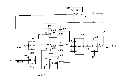
Fig. 1 is a block diagram showing the configuration
'f
a
- 19 - 2~92~'~7
of the integrator according to the first embodiment. In
this embodiment, the integrators shown in Fig. 5 are
composed of identical hardware and therefore the
integrator 306 will be described as being representative
S of these integrators. Figs. 10 and 11 are diagrams
showing examples of input/output of the integrator shown
in Fig. 1.
The integrator 306 is for the purpose of two-
dimensionally integrating the result xi,j (where i
represents a main-scan coordinate and j a sub-scan
coordinate) of the judgment made by the color-shade
matching circuit 310, thereby eliminating noise from the
result.
In Fig. l, numerals 501, 502 and 507 denote flip-
flops that hold data at the timing of the leading edge
of the CLK' signal. Numerals 503, 504 denote
multipliers to which two eight-bit signals are inputted
(at terminals A, B). Each of the multipliers 503, 504
multiplies these signals together and outputs an eight-
2 0 bit signal (256) as the result. Numeral 505 denotes a
multiplier to which a one-bit input signal (A) and an
eight-bit input signal (B) are applied. The multiplier
505 multiplies these signals together and outputs an
eight-bit signal (AxB) as the result.
2 5 Numeral 506 denotes an adder to which three eight-
bit signals are inputted (at terminals A, B, C). The
adder 506 adds these signals together and outputs an
eight-bit signal (A+B+C) as the result. This output
signal enters an eight-bit latch 507. Numeral 508
denotes, say, a FIFO (first-in first-out) memory which,
if n represents the number of pixels on one line,
applies a delay of n-1 pixels and outputs yi,j-1 when
Yi-l.j enters the FIFO memory.
The integrator of Fig. 1 is adapted so as to form a
filter. More specifically, the output of the eight-bit
latch 507 takes two paths. The output on one path is
fed back to the adder 506 via the FIFO memory 508, the
eight-bit latch 501 and the multiplier 504. The output
on the other path is fed back to the adder 506 via the
multiplier 503. That is, the filter output yi-1.j
enters the A terminal of the adder 506 via the
multiplier 503, and the filter input xi,j enters the B
terminal of the adder 506. Therefore, the filter of
Fig. 1 constructs a recursive-type IIR (infinite impulse
response) filter with respect to the impulse input xi,j.
2 0 Further, the filter output yi,j-1 of the preceding line
enters the B terminal of the adder 506 via the FIFO
memory 508. Accordingly, the filter of Fig. 1 acts as a
two-dimensional IIR filter, namely an IIR filter for the
directions i and j. The characteristic of the filter of
2 5 Fig. 1 is expressed as follows:
Yi, j = (x/256) ~yi-1~ j + (~3/256)Yi. j-1 + Y'xi-1, j . . . (1)
- 21 -
where a, (3 and Y represent constants that have been
preset. These constants act as weighting coefficients.
The various characteristics of the filter (integrator)
of Fig. 1 are decided by the sizes of these values.
That is, oc decides the contribution of integration in
the j direction (sub-scan direction), (3 the contribution
of integration in the i direction (main-scan direction),
and Y the contribution of the input data. For example,
in a case where Oc = 124, (3 = 124, y = 8 holds, an output
yi~~ of the kind shown in Fig. 11 is produced in
response to an input xi~~ of the kind shown in Fig. 10.
Here i (main-scan position) or j (sub-scan position) is
plotted along the horizontal axis. The horizontal axis
indicates similar characteristics whether viewed from
the main-scan cross section or sub-scan cross section.
In other words, the input xi~~ represents a two-
dimensional input.
An impulse input "1" regardless of the fact that
values on either side thereof are almost "0", as at
2 0 points 701, 702, and an impulse input "0" regardless of
the fact that values on either side thereof are almost
"1", as at point 703, may be considered to be noise.
When this is processed by the integrator 306 having the
circuit arrangement illustrated in Fig. l, an output
2 S yi~~ of the kind shown in Fig. 11 is obtained.
In the discriminating circuit 409 shown in Fig. 5,
- 22 -
the output yi,j from the integrator 306 and a threshold
value, which has been stored beforehand in the register
307, are compared by the comparator 308. Fig. 11
illustrates the threshold value 704 of the register 307
and the output yi~j of the integrator 306. The
comparator 308 uses the threshold value to binarize the
output yi of the integrator 306, thereby making it
possible to eliminate noise.
In other words, the integrator of Fig. 1 integrates
the data, which is indicative of the result of judgment,
in two directions, namely the main- and sub-scan
directions. As a result, continuity of the results of
judgment in the horizontal and vertical directions is
stressed, and results of judgment that are not
continuous in these two directions are eliminated as
noise.
Results of Processing
Fig. 12 is a diagram showing an example of the
results of copying according to the first embodiment.
2 0 In Fig. 12, numeral 801 denotes an example of a mixed
original. A part of this original contains a special
original 803 to be discriminated by the apparatus of the
invention. If the original 801 containing the special
original 803 is copied, an outputted result of the kind
2 5 shown at numeral 802 is obtained. In the result 802,
the portion corresponding to the special original 803
,.
J
1
- 23 - 2fl92~7'~
becomes a masked image 804. For example, the masked
image 804 is formed in the color magenta (M) when CNO =
0 holds, the color cyan (C) when CNO = 1 holds, the
color yellow (Y) when CNO = 2 holds and the color black
(Bk) when CNO = 3 holds. As a result, the portion
corresponding to the special original 803 cannot be
copied normally.
RAM Data Updating Procedure
The data in the color-shade matching LUT 302 should
not be readily modifiable in nature. If anyone were
capable of modifying the data in the LUT at will, this
might make it possible for the apparatus to be used
unlawfully in the falsifying of bank notes, securities,
etc. Accordingly, in the present invention, an IC card
containing data that is difficult to falsify is
employed, and a pass word that generally is not
disclosed is required to be entered from the operating
unit 420 in order to alter the data in the LUT 302.
This makes it possible to avoid the danger of
2 0 falsification.
Fig. 13 is a top view showing the control panel of
the operating unit 420 according to the first
embodiment. The operating unit 420 is disposed on the
front side of the apparatus.
2 5 As shown in Fig. 13, the control unit 420 includes
a numeric key pad 902, a copy starting key 903 for
24
starting a copying operation, a reset key 904 for
initializing various set modes, and a liquid-crystal
display unit 905 equipped with a touch panel for setting
various modes.
Entry of the pass word is performed by using the
numeric key pad 902. More specifically, a pass word
desired to be set is entered as follows:
[*] [2] [0] [4] [2] [9] [C] [*]
Fig. 14 is a flowchart for describing the procedure
1~ for rewriting the color-shade matching LUT 302 according
to the first embodiment. The processing of Fig. 14 is
executed by the CPU 414, the program whereof is stored
in the ROM 415.
First, at step S1001 in Fig. 14, it is determined,
based upon a signal from the card reader 228, whether
the prescribed IC card has been inserted. If the
prescribed IC card has been inserted, the program
proceeds to the next step 51002, at which it is
determined whether the pass word has been entered by the
2 0 numeric key pad 902. If the pass word has not been
entered correctly, the program returns to the initial
step. If the pass word has been entered correctly, then
the information in the color-shade matching LUT 302 is
updated at step 51003.
2 5 Thus, in accordance with the first embodiment as
described above, judgment data extracted from read image
25
data is passed through a filter that performs an
integrating operation in two dimensions, thereby making
it possible to correctly obtain judgment results, which
indicate whether an original is a special original or
not, without being affected by the direction or
orientation of the original image. In addition, by
constructing the filter as a so-called two-dimensional
IIR filter, two-dimensional noise components in the
judgment data are reliably eliminated so that it is
possible to correctly obtain judgment results that
indicate whether an original is a special original or
not.
<Discriminating Circuit> Second Embodiment
The integrating circuits 303-1 ~ 303_g in the
1$ discriminating circuit 409 of Fig. 1 each possess the
FIFO memory 508 in order make possible integration in
the j direction. However, providing the FIFO memory
enlarges the scale of the circuitry and raises cost.
The discriminating circuit according to the second
2 0 embodiment described below is so adapted that the eight
integrators share a single FIFO memory.
Fig. 15 is a block diagram showing the
discriminating circuit according to a second embodiment
of the invention, and Fig. 16 is a block diagram showing
2 5 the configuration of the integrator according to a
second embodiment. Elements in Fig. 15 identical with
26 _
those shown in Fig. 3 are designated by like reference
characters and need not be described again.
A comparison of Figs. 5 and 15 reveals that the
discriminating circuit of the second embodiment differs
from that of the first embodiment in the construction of
the integrator; there is no difference with regard to
the thinning-out circuit 301, frequency dividing circuit
305 and color-shade matching circuit 310. More
specifically, as shown in Fig. 15, numeral 1101 denotes
an integrator corresponding to the integrator 306 (Fig.
5) of the first embodiment. The details of this
integrator are shown in Fig. 16. In Fig. 15, numeral
1102 denotes a serial/parallel converter, 1103 a
parallel/serial converter, and 1104 a FIFO memory
similar to the FIFO memory 508. Further, numerals
1303-1 ~ 1303_g denote color-shade judging circuits
composed of identical hardware. Each circuit comprises
the integrator 1101, a register 1307 and a comparator
1308 and each judges whether a special original is
2 0 contained in an original.
The outputs of the eight integrators 1101 of the
eight judging circuits 1303 enter respective X1 ~ Xg
terminals of the parallel/serial converter 1103. The
eight items of eight-bit data that enter the converter
2 5 1103 as parallel data are converted into eight blocks of
successive serial data, in which each block is composed
_ 27
of eight bits. This data enters the FIFO memory 1104,
where the data is delayed by one line before being
inputted to the serial/parallel converter 1102. The
continuous serial data composed of eight blocks (one
block = eight bits) outputted by the FIFO memory 1104
enters the X terminal of the converter 1102, which
converts this data into eight items of parallel eight-
bit data and delivers the converted data to terminals
Y1 ~ Yg. Thus, the single FIFO memory 1104 is capable
of being shared by the eight judging circuits.
Fig. 16 illustrates the configuration of the
integrator 1101 according to the second embodiment.
Since the eight judging circuits (1303-1 ~ 1303-g) share
one FIFO memory, this arrangement differs from that of
Fig. 5 in that it does not possess a FIFO memory.
Parallel/Serial Converter 1103
Fig. 17 is a block diagram showing the
configuration of the parallel/serial converter 1103
according to the second embodiment. As shown in Fig.
2 0 17, the converter 1101 includes an 8-to-1 selector 1319,
a three-input OR gate 1320, a three-bit counter 1321,
and an inverter 1322. The parallel/serial converter
1103 includes eight mean-value arithmetic circuits
(1301, 1302, ~~~, 1308), which have terminals X1 ~ Xg,
2 S respectively, for calculating the mean value of the
eight-bit data applied to the respective terminal.
28
Eight-bit data from each of the eight mean-value
arithmetic circuits (1301, 1302, ~~~, 1308) enters the
selector 1319 which, in eight operations, successively
outputs the eight items of eight-bit data in order.
Each individual mean-value circuit has seven eight-
bit latches (1309, 1310, 1311, 1312, 1313, 1314 and
1315), a mean-value circuit 1316, a two-input selector
1317 and an eight-bit latch 1318. The seven eight-bit
latches (1309, 1310, 1311, 1312, 1313, 1314 and 1315)
latch the input data in synchronism with the leading
edge of CLK', thereby subjecting the input data to a
delay equivalent to one pulse of CLK'. The mean-value
circuit 1316 outputs the mean value (~Xi/8) of the eight
inputs at terminals X1 ~ Xg. In effect, this output is
the mean value of eight successive input signals. In
other words, one mean-value arithmetic circuit 1301
outputs the mean value of the results of judgment
regarding one color shade for eight consecutive pixels.
The parallel/serial converter 1103 outputs, in order,
2 0 the mean values (eight bits each) of the results of
judging eight types of color shades (of eight
consecutive pixels each).
Fig. 18 is a timing chart showing the operation of
the parallel/serial converter 1103.
2 5 The three-bit counter 1321 outputs a signal XCNT,
which is initialized by the signal HSYNC and
- 29 -
synchronized to the leading edge of CLK', repeatedly
takes on the values 0, 1, 2, 3, 4, 5, 6, 7. A signal
XSEL produced by the gate 1320 becomes "0" only when the
signal XCNT is "0" and is "1" at all other times (i.e.,
when XCNT is not "0"). The mean value of eight
consecutive input signals a, b, c, d, e, f that enter
the terminal X1 of the parallel/serial converter 1103 is
applied to the X1 input terminal of the selector 1319
(Fig. 17) as ml at the timing illustrated. Similarly,
the mean values of the consecutive eight input signals
that enter the terminals X2 ~ Xg of the parallel/serial
converter 1103 are applied to the input terminals X2
Xg of the selector 1319 as m2 ~ mg. Furthermore, since
the signal XCNT enters the control-input terminal S of
the selector 1319, the mean values m1 ~ m8 are outputted
in successive fashion, as illustrated in Fig. 18.
Serial/Parallel Converter 1102
Fig. 19 is a block diagram showing the
configuration of the serial/parallel converter 1102
2 0 according to the second embodiment. As shown in Fig.
19, the converter 1102 includes seven eight-bit latches
(1501, 1502, 1503, 1504, 1505, 1506, 1507 that) latch
input data A in synchronism with the leading edge of
CLK', thereby subjecting the input data X to a delay
2 5 equivalent to one pulse of CLK'. Also included are a
2-to-1 selector 1508 and a flip-flop 1509. The signal
- 30 -
XSEL is identical with the signal XSEL shown in Figs. 17
and 18.
Fig. 20 is a timing chart showing the operation of
the serial/parallel converter 1102.
The serial/parallel converter 1102 synchronizes the
eight consecutive inputs a, b, c, d, e, f, g, h to the
signal XSEL and outputs the data from terminals Y1 ~ Y8
in parallel fashion.
Figs. 21, 22 and 23 are diagrams for describing, in
specific terms, the results of the operation performed
by the integrator 1101 according to the second
embodiment. Fig. 21 is a diagram showing the input
signal xi,~ that appears at the X1 terminal of the
integrator 1101 (see Fig. 15), Fig. 22 is a diagram
showing the output signal yi,~ that appears at the Y
terminal of the integrator 1101, and Fig. 23 is a
diagram showing the feedback input signal y'i,~, from
the FIFO memory 1104, that appears at the X2 terminal of
the integrator 1101.
2 0 First, in a case where the binary (one bit)
decision signal xi~~ (see Fig. 21) enters the terminal
X1 of the integrator 1101, yi~~ (see Fig. 22) appears at
the Y output of the integrator 1101. In the first
embodiment described above, the value of yi~~ is delayed
in the sub-scan direction by the FIFO memory 508 and
then enters the integrator 306 again. In the second
_ 31 _ 2~~28'~~
embodiment, however, the mean value of eight consecutive
items of data is delayed by one line in the sub-scanning
direction by the FIFO memory 1104 and then enters the X2
terminal of the integrator 1101 as y'i~j (Fig. 23).
Since the output of the integrator 1101 naturally
does not possess many high-frequency components,
substantially the same output is presented even if the
eight consecutive items of data are interchanged for
their mean values. As a result, the number of items of
data accumulated in the FIFO memory 1104 are thinned to
1/8. By utilizing this, an integrator having a function
equivalent to that of the integrator requiring eight
FIFO memories in the first embodiment can be constructed
using a single FIFO memory.
<Modification>
The present invention can be modified in various
ways without departing from the scope of the claims.
For example, though the number of bits constituting
the image data is 15 bits for the colors R, B, G in the
2 0 foregoing embodiments, the number of bits of image data
may be selected at will. Though eight color shades are
judged in the foregoing embodiment, the invention may be
applied to any number of color shades.
Further, in the first embodiment, the integrator is
2 5 constituted by an IIR filter, but this may be replaced
by an FIR filter.
32
The present invention is applicable also to an
image processing system having a plurality of the image
processing apparatus according to the foregoing
embodiments. Though the data processing in the
foregoing embodiments is executed entirely by hardware,
the processing can be executed by a program and the
invention covers such a modification.
Further, in each of the foregoing embodiments, a
laser-beam printer has been described as an example of
the apparatus. However, the invention is not limited to
a laser-beam printer but can be applied to an ink-jet
printer or thermal-transfer printer as well. In
particularly, the invention is applicable to a so-called
bubble-jet printer using a head of the type that
1$ discharges droplets by means of thermal energy.
In each of the foregoing embodiments, the original
image is entered by a reader. However, this does not
impose a limitation upon the invention. The invention
can be applied to an image entered by a still-video
2 0 camera or an ordinary video camera or to an image
created by a computer graphics technique.
As many apparently widely different embodiments of
the present invention can be made without departing from
the spirit and scope thereof, it is to be understood
2 5 that the invention is not limited to the specific
embodiments thereof except as defined in the appended
-33-
claims.