Note : Les descriptions sont présentées dans la langue officielle dans laquelle elles ont été soumises.
2 ~ 9 3 ~ 2 5 o.z. 0050/43148
Analysis of the physical proPerties of thin layers
and electro-optically active thin layers
The present invention relates to a method of
analysing the physical properties of thin electro-
optically active layers using polarized light.
DE-A 39 14 631 Al discloses a method of analysing
the physical properties of thin layers with the aid of
polarized light, in which the layer or layer system to be
analysed is irradiated and the reflected light or the
transmitted light is diverted into an imaging system. It
has also been disclosed that nonlinear optically active
thin layers can be analysed with the aid of integral
methods. However, these methods have the disadvant~ge
that the result of the analysis is an average over the
entire wavelen~th region of the incident light, which is
detected by means of a photodiode.
Imaging optical methods for analysing and charac-
terizing the physical properties of surfaces are of
interest in many areas of industry. In particular,
methods of analysing thin and ultrathin electro-optically
active dielectric layers having thicknesses of from a few
microns down to the sub-nanometer range are increasingly
in demand in physics, chemistry, information processing
and photonics. The aim of the invention is to display
surface structures and the distribution of the functional
properties with maximum lateral resolution and high
contrast.
For analysis of thin and ultrathin layers in high
contrast, the optical waveguide microscope, as described
in DE-A 39 14 631 A1, is known. However, this method has
the disadvantage that additional heterogeneities in the
electro-optical layer caused by the polarization process
cannot be detected. Analysis by the integral methods of
Cross (G.H. Cross, I.R. Girling, I.R. Peterson und N.A.
Cade, Electron. Lett. 22 (1986) 1111), Levy (M. Dumont,
Y. Levy und D. Morichere, Organic Molecules for Nonlinear
Optics and Photonics. Edited by J. Messier, NATO ASI
~3~`?~
- 2 - o. z . 0050/43148
Series, Kluwer Academic Publisher, 1991) and Swalen (R.H.
Page, M.C. Jurich, B. Reck, A. Sen, R.J. Twieg, J.D.
Swalen, G.C. Bjorklund and C.G. Willson, J. Opt. Soc.
Am. B, 7 (1990) 1239) only allow an averaged determina-
tion of the electro-optical behavior. Comprehensive
quality monitoring is thus not possible.
It is an object of the present invention to
provide a simple method of analysing thin and ultrathin
layers and layer systems for surface structures, refrac-
tive index structures and polarization structures, ie.
the alignment distribution of the functional units, in
high intensity contrast, ie. high vertical resolution,
and good lateral resolution.
We have found that, surprisingly, this object is
achieved by a method of analysing the physical properties
of thin layers with the aid of polari~ed light, in which
the layer or layer system to be analysed is irradiated,
and the reflected light or the transmitted light is
diverted onto an imaging system, which comprises exposing
the layer or layer system to be analysed to polarized
light in order to excite waveguide modes which, due to
the applied modulated electrical field, reproduce lateral
differences in the electro-optical (EO) properties of the
sample to be analysed.
The layer or layer system to be analysed can have
been applied to any surface of a solid, for example a
metal layer or semiconductor layer.
In order to excite waveguide modes in the layer
or layer system to be analysed, a coupling arrangement is
preferably used~
The preferred coupling arrangement is a prism, in
which case the layer or layer system to be analysed is
applied directly to the prism base coated with a metal
film or semiconductor film.
However, the coupling arrangement may alterna-
tively and advantageously be a grating structure on the
surface of a solid, where the layer or layer system to be
2~93~2~
- 3 - O.~. 0050/43148
analysed has been applied to a transmitting and electro-
conductive layer (for example ITO) applied to the grating
in advance.
In order to image the nonlinear electro-optical
effect, two electrodes are applied to the layer or layer
system to be analysed. The metal- or semiconductor-coated
prism base on one side of the layer or layer system to be
analysed preferably serves as an electrode. A counter-
electrode is applied directly to the opposite side of the
layer or layer system to be analysed.
However, the counterelectrode is preferably
separated from the layer or layer system to be analysed
via insulating spacers, eg. Mylar films.
The two electrodes are advantageously applied
alongside one another to the layer or layer system to be
analysed. This allows a waveguide structure to be written
in at the same time as the polarization process.
Surprisingly, the novel method allow~ simple
analysis of surface structures, refractive index struc-
tures and polarization structures on layers having thick-
nesses of from 0.1 nm to about 1 mm.
Waveguide modes in thin transparent media are
discussed by P.K. Tien in Rev. Mod. Phys. 49 (1977) 361.
These are electromagnetic waves which are able to propa-
gate in transparent thin media. The wave propagates
parallel to the surfaces of the medium and is attenuated
in the propagation direction. The electromagnetic field
drops expotentially at the surface of the medium.
Waveguide modes in thin dielectric electro-
optically active layers can be excited using essentially
two coupling arrangements: prism coupling (cf. P.K. Tien,
R. Ulrich, Appl. Phys. Lett. 14 (1969) 291) and grating
coupling (cf. D.G. Dalgoutte, C.D.W. Wilkinson, Appl.
Optics, 14 (197~) 2g83).
In the case of prism coupling, parallel- (= p) or
perpendicular- (= s) polarized light is incident on a
prism and is totally reflected at the prism base. The
2~93~2~
- 4 - O.Z. 0050/43148
waveguide layer or layer system to be analysed is applied
to the prism coated with a metal layer or semiconductor
layer, and is provided with a counterelectrode. An
appropriate choice of the angle of incidence of the light
causes a waveguide mode to be excited in the layer or
layer system to be analysed. The intensity of the reflec-
ted light beam reaches a minimum at this angle.
In the case of grating coupling, the surface of
a solid is modulated in the form of a line grating by
embossing or etching. A transmitting and electroconduc-
tive layer is applied to this modulated surface, the
layer or layer system to be analysed then applied, and
this is then provided with a counterelectrode. As in
prism coupling, a waveguide mode can be excited in the
layer or layer systems to be analysed at a suitable angle
of incidence of the p- or s-polarized light. The inten-
sity of the reflected light again reaches a minimum at
this angle.
Lateral structures of a layer or layer system to
be analysed result in different coupling conditions for
waveguide modes. If polarized light is incident at a
fixed angle on one of the above-described sample arrange-
ments, lateral structures of the layer or layer systems
to be analysed can be detected from the different reflec-
tion, ie. their different brightnesses. Variation of the
angle of incidence allows the coupling condition to be
satisfied at different angles for different areas of the
layer or layer system to be analysed, allowing lateral
structures to become visible.
The lateral resolution is affected by the attenu-
ation of the waveguide mode. Attenuation of a waveguide
mode is determined by the absorption and quality of the
surfaces of the waveguide medium itself and the absorp-
tion of the adjacent modes. For good lateral resolution,
the attenuation of the waveguide mode should be very
high.
The vertical resolution is in the sub-nanometer
2~93~2~
- 5 - O.Z. 0050/43148
range, ie. thickness differences of less than 1 nm in a
waveguide layer result in significantly different reflec-
tion and thus observable contrast.
If an electrical field is applied to the layer or
layer system to be analysed, a change in refractive index
of the electro-optically active system can be observed
due to the good resolving power. The electrical field
changes the electron density distribution of the pola-
rized system and thus causes a change in the refractive
index of the system. This change results in a shift in
the minimum angle of the mode, which is evident from a
change in contrast. It is thus possible to detect not
only the lateral and vertical structure of the layer or
layer system to be analysed, but also the quality of the
polarization-induced electro-optical effect, which is a
function of the alignment distribution of the chromo-
phores in the system. Monitoring for a homogeneous
distribution of the functionalized properties in the
layer is thus possible.
The apparatus to be used according to the inven-
tion for analysis of the physical properties of thin
layers has a simple mechanical and optical structure. It
may be regarded as an electro-optical microscope. Prism
coupling is preferred for the generation of waveguide
modes. A specimen slide is bonded to the prism surface by
means of immersion fluid, a metal layer is applied to the
reverse of the slide, and the layer or layer system to be
analysed is applied to the metal layer. An alternative
procedure is to apply both the metal layer and the layer
or layer system to be analysed directly to the prism
surface. An electrode of the same metal is applied
directly to the other side of the layer or layer system
to be analysed. Suitable metals here are silver, gold,
copper and aluminum, or layer systems of these metals.
The use of a layer system which comprises from 2 to 5 nm
of chromium and 45 nm of gold has proven particularly
advantageous. The resultant mirror is illuminated by
2~93~
- 6 - O.Z. 0050/43148
means of parallel monochromatic, colored or white p- or
s-polarized light at a flat angle through one of the two
free sides of the prism and imaged with the aid of an
achromatic lens of small focal length which is focused
on the mirror, through the other free side of the prism
onto a screen, a video camera or an eyepiece. The coun-
terelectrode is likewise applied as a layer system
comprising from 2 to 5 nm of chromium and 100 nm of gold.
The two electrodes are contacted using conductive silver
and connected to a function generator.
Suitable layers for analysis are thin dielectric
layers (for example organic polymers, copolymers or
elastomers which have been mixed with NLO dyes) which
have been structured with respect to refractive index,
thickness and electro-optical function. Thése layers
have, for example, a thickness of from 100 nm to l mm.
The layers can be applied to the metal layer by, for
example, spin-coating or by the Langmuir-Blodgett-Kuhn
(LBK) method. In addition, layers having a thickness of
from 0.1 to 100 nm which have been structured with
respect to refractive index, thickness and electro-
optical function can be analysed. To this end, a wave-
guide dielectric layer is expediently first applied to
the metal, for example by spin-coating or by the LBK
method, and the layer to be analysed is applied to the
first layer, for example by the L~K method, spin-coating,
adsorption from the liquid phase, casting or vapor
deposition.
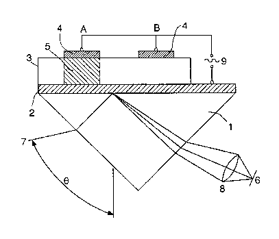
Figure 1 shows a diagrammatic representation of
the structure of an apparatus used for the novel method.
An electrode 2 is vapor-deposited onto the base
of a 90 glass prism (BK-7) 1, which serves as a wave-
guide coupler in a Kretschmann arrangement. A thin non-
linear electro-optically active film 3 is spin-coated
onto the electrode 2. After the layer has dried, two
electrodes 4 are vapor-deposited as top electrodes. The
area 5 beneath the electrode A is polarized at above the
~3~2~
- 7 - O.Z. 0050/43148
glass transition temperature using a direct-current
voltage. The area B serves as the unpolarized reference
channel. The two areas are imaged via a TV camera 6,
which records the reflected light from a laser 7 as a
function of the angle of incidence. The images imaged on
the TV camera 6 by means of a simple lens 8 are recorded
on magnetic tape. In an electro-optically active layer
(area A), the distribution of the electro-optical effect
can be observed by applying an electrically modulated0 field 9 between the two electrodes 4 and 2.
EXAMPLE
The layer system to be analysed is composed of
the gold electrode 2 having a thickness of d = 51 nm and
the polymer film 3 comprising a guest-host matrix of PMMA
(polymethyl methacrylate~ and 10% by weight of Disperse
Red 1 ((4-(N,N'-ethylethanol)amino-4'-nitroazobenzene,
DR 1). The polymer film 3 was spin-coated onto the gold
electrode 2 from a 20~ strength 2-ethoxyethyl acetate
solution. After the polymer layer 3 had dried (T = 80,
12 hours under reduced pressure), the top electrodes 4
were applied in a width of about 5 mm onto the polymer
film 3. The area A was subsequently polarized above Tg at
110C with application of a direct-current field of E =
100 V/~m. In order to indicate the sensitivity of the
analysis method, the sample was left to relax for one
week. Figure 2 shows the image section of a polymer film
3 excited by means of p-polarized light. 10 is the
unpolari~ed area B covered by the top electrode, ll is
the uncovered polymer film and 12 is the gold-covered
polarized area A. The dark region indicates that the
reflected intensity of the HeNe laser (633 nm) 7 has a
minimum, ie. an optical waveguide mode has been excited.
Application of an electrically modulated field 9 to the
electrodes causes a difference in the reflected intensi-
ties of the polarized and unpolarized fields. This iseasily visible with the naked eye and can be demonstrated
by gray value analysis of the recorded images. The
- 8 _ 2~9 3 ~ ~050/43148
relevant data are shown in Figure 3. Before the 0.95 Hz
and 220 V (tip-tip) field is switched on, a slight
difference in the intensity of the unpolarized (open
symbols) and polarized (solid symbols) states is evident.
This depends on the coupling angle ~. The data shown by
a circle were recorded at an angle of incidence of ~ =
58.8, and the data shown by triangles were recorded at
an angle of ~ = 59.3. The difference between the two
areas becomes clear here when the modulated voltage is
applied; whereas the electro-optical behavior of the
polarized area, as evidenced by the reflected intensity,
follows the electrical signal, the unpolarized area
remains at constant intensity. This is shown in Figure 3,
in which the mean gray values obtained by analysis of
every second image, corresponding to a time interval of
1/30 second, have been plotted.