Note : Les descriptions sont présentées dans la langue officielle dans laquelle elles ont été soumises.
2~~6 ~~~
METHOD OF FORMING CLOSELY-SPACED, GENERALLY PARALLEL
SLOTS THROUGH A THIN WALL AND PRODUCT FORMED THEREBY
Technical Field
The present invention deals broadly with the field of
machining through relat;ively.'thin walls of components. More
narrowly, however, it is directed, in one specific application, to
machining and manufacturing a housing for mounting a plurality of
connector elements which are to be engaged by corresponding
contacts of, for example, an integrated circuit, which are disposed
in an array. The focus of the invention is a method of
manufacturing such a product wherein a plurality of generally
parallel slots are formed through the, wall, each slot being
intended to receive one connector element.
Background of the Invention
Various applications exist wherein closely-spaced slots ere to
be defined through a relatively thin wall in the manufacture of a
particular product. One specific example of an application is a
connector housing for mounting a plurality of connector elements
used in integrated circuit testing. The electrical connector
elements are, typically, generally planar in configuration and are
mounted in substantially parallel slots for rotation about an axis
generally perpendicular to planes defined by the elements. The
rotation is effected as contacts of the integrated circuit engage
the connector elements, and a "wiping" action is thereby effected
so that, at the interface between a connector element and a contact
of the integrated circuit, a good electrical transmission path is
established.
The spacing of the connector elements is, of course, dictated
20~~~~'~
by the spacing of the contacts on the integrated circuit to be
tested. Very frequently, the spacing is quite close. It is
necessary, therefore, to provide'~slots in the housing mounting the
electrical connectors which are spaced at the appropriate distances
in view of the contact spacing on the IC.
The housing for mounting the connector elements, as will be
able to be seen then in view of the disclosure to this point,
provides an array of alternating slots arid ribs. Typically, in
view of the close spacing of the contacts on the IC, the ribs are
very narrow. They are often only on the order of a range between
0.005 to 0.035 inches in thickness. In many cases they are less
than 0.025 inches thick.
' The problems in manufacturing a housing as~ discussed
hereinbefore are complicated by the manner in which the connector
elements are mounted in the housing. United States Patent No.
5,069,269, which issued to the present Applicant on December 3,
1991, illustrates elongated tubular elements, which can be either
elastomeric or rigid in nature, which are received in troughs
formed in oppositely facing surfaces of the generally thin wnll of
the housing. The connector elements illustrated in that patent
are, in turn, hooked to the tubular members to accomplish mounting.
It will be seen then that it is frequently necessary to provide a
trough or troughs which run across the arrny of slots iri which the
connector elements are disposed.
The prior art has sought to provide appropriate manufacturing
processes fox a housing for mounting the electrical connector
2
209602
elements. A first proposed solution has been to form the housing ".
employing an injection molding process. This has been the standard
method for producing a low cost housing component for test sockets
for semiconductor devices. Injection molding does, however, have
economic, technical, and leadtime drawbacks. Tooling and
developing costs incident to the injection molding of a housing can
run ae high as $90,000 dollars. The specific costs, of course,
depend upon a number of factors including. the number of connector
elements to be provided for mounting. From a technical
perspective, however, injection molding almost becomes precluded in
view of the minute dimensions typically involved. In view of the
very thin width dimension of ribs between connector element
mounting slots (typically less than 0.025 inches), the material
used for molding and the pressures required to inject the material
make it virtually impossible to provide an acceptable product using
this method.
Such a housing requires close tolerances. In the case of
injection molding, dimensional accuracy is sacrificed. The
material injected has some measure of shrinkage associated with tha
injection molding process, and such shrinkage becomes clearly
evident after the housing is cured.
The second manufacturing possibility is water-jet cutting.
Such a method, however, typically, produces a poor slot cut along
the full length of each slot. Problems are typically encountered
with the initial penetration of the water-beam. The initial
penetration typically causes an enlarged hole. Further, however,
3
2(~~~~~~
. __,
the housing material, in the case of water-jet cutting, chips and
fractures.
Another proposed solution is tool machining. Such a
possibility is, however,,unacceptable for a number of reasons. A
housing takes too long to manufacture, and the probability of tool
bits breaking is high. Even when bits do not break, the ribs
defining the slots in the housing can deform during the
manufacturing process. Such deformation: occurs because of tool
pressure causing the ribs to deflect.
Another potential solution to the manufacture of such a
product is laser machining. Laser machining of plastics has been
performed in numerous applications for a number of years. Limited
success has been achieved with respect to high-temperature
engineering plastics.
One of the major drawbacks to laser cutting of any engineering
plastic is that a char residue can remain on the surface of the
~ material that has been machined. Such a residue is, on occasion,
electrically conductive. This is particularly unacceptable in the
case of the manufacture of an electrical connector housing.
Other questions have remained with regard to utilization of
laser machining such components. Should the connector element
slots be formed first and then troughs for receiving tubular
mounting members farmed thereafter? It has been found that, by
doing so, the slots tend to have rolled edges and machine burrs
which are almost impossible to remove.
It ie to these dictates and problems of the prior art that the
4
~~~~r~
present invention is directed. It is an improved method for --
manufacturing a product such as an electrical connector housing for
mounting a plurality of connector elements.
Summary of the Invention
The present invention is,'a method of manufacturing a product
in which a plurality of closely-spaced, generally-parallel slots
are to be formed through, or partially through, a thin wall of a
block, typically, of a plastic material:' The method includes a
step of filling one or more troughs formed in one or both of
oppositely facing surfaces of the wall with a filler material to
form a rod. Such a rod conforms in cross~section, generally, to a
cross-section of the trough. With the rod or rods received within
the trough or troughs, a plurality of generally parallel slots are
laser machined through the wall of the block across the filled
trough or troughs. When such troughs are present, the slots are
machined so as to intersect one or more corresponding troughs.
After the slots are laser machined through the wall, the disc-like
residual rod portions are removed from the troughs. In a preferred
embodiment of the process, a block made of a polyamide-imide
material is provided to be machined, it is envisioned that a
thickness of the wall through which the slots are to be machined
would be lees than about 0.15 inches. In this application, one or -
more troughs would be provided in at least one of the~oppositely
facing surfaces of the wall.
In this embodiment, after machining of the slots has been
accomplished and disc-like residual rod portions in the troughs
2o~s~sz
have been removed, the component thereby manufactured is cleaned.
Cleaning can be accomplished by directing a stream of glass
particles from a small tip opening nozzle into the slots.
Concurrently, a dry gas Gan be directed into the slots to reduce
moisture and, thereby, the possibility that the glass particles
will clog up the slots. By utilizing such steps, the slots can be
abrasively cleaned of a black char deposit which is typically left
after the laser machining step is performed.
The slotting process, typically, takes a number of pulses to
completely form the slot. The laser pulse, in the case of most
laser machining implements, produces a small diameter hole.
Typically, the hole is on the order. of between 0.003 to 0.007
inches in diameter. Frequently, it is necessary to induce two
pulses, at least in forming the first hole, to completely burn,
through the thickness of the wall when the wall is, for example,
0.090 inches thick. One pulse might, of course, be sufficient with
thinner walls.
Pulsing of the laser at different locations is thereby
sequentially accomplished to fully define the slot. Overlapping
holes are formed to extend the length of the slot. Holes which
overlap on the order of 0.001 inches to 0.002 inches have been
found to be appropriate when the laser beam diameter is between
0.005 inches and 0.007 inches. With such a beam diameter, any
smaller overlap would result in "scalloping". If the overlapping
were any greater, an excessive amount of heat would be allowed to
build up in the material, and warping of the ribs between the slots
6
2~~6~62
could result.
The present invention is thus an improved method for
manufacturing a structure as discussed. More specific features and
advantages obtained in view of those features will become apparent
with reference to theDETAILED DESCRIPTION OF THE INVENTION,
appended claims, and accompanying drawing figures.
Brief Description of the Drawing
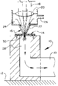
Figure 1 is a simplified mechanical.~diagram of a structure
used in accordance with the present method invention with
projection lines and arrows added for descriptive purposes;
Figure 2 is an enlarged simplified mechanical diagram of the
structure shown in Figure 1;
Figure 3 is a fragmentary pictorial view of a preprocessed
workpiece;
Figure 4 is a fragmentary pictorial view of the workpiece of
Figure 3 after slots have been laser machined into the workpiece;
Figure 5 is a fragmentary top plan view of the workpiece with
filler material removed from troughs; and
Figure 6 is a sectional view taken generally along line 6-6 of
Figure 5.
Detailed Description of the Invention
Referring now to the drawing wherein like reference numerals
denote like elements throughout the several views, Figure 1
illustrates, in a simplified presentation, an alignment fixture 10
which is mounted to an X-Y coordinate table 12. The alignment
fixture 10 can be disposed so that it is moved, as dictated by
7
209~~~2~
computer programming, such that, for example, a test socket housing
14 secured on the fixture 10 ie moved relative to a fixed laser
head 16.
A laser beam 18 is .generated at a source (not shown) and ie
focused by a lens 20 to a concentrated beam as at 22. The lens 20
is mounted within a chamber 24 closely proximate the test socket
housing 14 to be machined.
An inert gas.(for example, Nx) can.'be introduced into the
chamber 24 through a fitting 26. The gas can function to purge the
chamber 24 so as to reduce the possibility of soot accumulating on
the lens 20. Additionally, this process helps urge soot and debris
from the laser cutting evolution downwardly through a passage 28 in
the alignment fixture 10 into a vacuum chamber 30. A vacuum is
applied through the alignment fixture 10 to pull smoke and debris
from the area of the component being machined.
The description to this point is of structure old in the art.
Loser equipmente for machining components, including plastic
components, are known. Using such equipment to machine plastics
has been done for a number of years, although such processes have
met with only limited success particularly with respect to high-
temperature engineering plastics.
The workpiece 14 shown in the figures as being mounted to the
alignment fixture 10 is a block intended to eventually function as
the housing for a test socket. Various materials have been used
for such housings in the prior art. Once such material is an
acetal material marketed under the name DELRINd. This material has
8
~o~s~s~
been found, however, to be not particularly appropriate for use in
the present process invention.
A material that is particularly appropriate is a polyamide-
imide material. One ,material of this nature which serves
particularly well is marketed under the name TORLON~. This
specific material is produced by Amoco Torlon Products Division of
Amoco Chemical Corporation. This specific material has been found
to have particularly good characteristics~'for being processed in a
manner as will be discussed hereinafter, and this is particularly
true when the material is glass-filled from between 10% - 40%.
Thinner~ribs between slots machined can be cut, and a cleaner cut
surface can be maintained.
An acceptable alternative material for use in this process is
one characterized as a polyether-imide resin. A specific material
within this alternative category is one marketed under the name
ULTEMA. This specific material is sold by General Electric.
Again, 10% - 40% glass filling enhances the material's
characteristics.
As seen in Figures 1-6, the test socket housing block 14 is.
provided with a relatively thin wall 32 defined by two oppositely
facing surfaces 34, 34'. The surfaces 34, 34' are spaced from one
another, typically, at a distance so that the thickness of the wall
32 if about less than about 0.15 inches. In some applications, the
thickness of the wall 32 could be even less than about 0.10 inches.
The thickness of the wall 32 selected will, of course, depend upon
a number of factors. Among these are the size of connector
9
20~~~62
elements (not shown) intended to be mounted in the test socket - .
housing 14.
Typically, when the wall 32'is on the order of 0.15 inches in
thickness, it will take two pulses of the laser, at least
initially, at the same,~,location to provide an aperture which
extends fully through the thickness of the wall 32. On the other
hand, however, when the wall 32 is 0.10 inches or less in
thickness, a single laser pulse may be sufficient to cut through
the full thickness of the wall 32.
It will be understood that slots to be cut, as illustrated in
Figures 4-6, will be formed by cutting multiple, adjacent apertures
through the thickness of the wall 32. Again, the alignment fixture
can be programmed so as to move in accordance with computer
software instructions to effect the cutting of a slot or slots 36
of the appropriate length and width. To do this, a series of
aligned, overlapping apertures would be cut through the wall 32,
and, if the application dictated the need for wider slots 36,
multiple rows formed by cutting aligned, overlapping apertures
could be effected.
In order to fully define the slot 36, the laser head 16 will
be pulsed at different locations in a sequential manner., Hoies
which are overlapped are formed to extend the length of the slot
36. Holes which overlap on the order of 0.001 inches to 0.002
inches have been found to be appropriate when the laser beam 22
diameter is, for example, between 0.005 inches and 0.007 inches.
Such a degree of overlapping will be sufficient so ae to preclude
2Q9~~~2
"scalloping". The overlapping will not be so extensive that an
excessive amount of heat builds up in the material. If such a
situation were allowed to occur, the ribs 38 between which the
slots 36 were to be defined could become warped.
It will be understood, however, that, prior to machining the
slots 36 as discussed to this point with a laser implement, one or
more troughs 40 could be formed in each of the two oppositely
facing surfaces 34, 34' defining the wall 32 in the housing block
14. These troughs 40 are best seen in Figures 3 and 4, and each
trough 40 ie intended to receive, when the workpiece being
processed is intended to serve as a test socket housing, a support
by which one or more connector elements are mounted within the
housing 14.
The supports (not shown) are intended to be generally tubular,
and the troughs 40 are shown as being defined by a pair of
generally parallel walls 42 merging, at the bottom of the
particular trough, with opposite edges of a generally semi-
cylindrical portion 44 of the trough 40. A support can, thereby,
be easily slipped into its respective trough 40, the diameter of
the support being substantially the same as the distance between
the generally parallel walls 42 defining, in part, the trough 40.
Prior to the performance of the laser machining operation, a
filler material such as a paste can be inserted into trough 40
across which slots 36 are to be cut. When the material dries, it
forms a rod 46. By providing such a rod 46, the slot 36 machining
process is more efficiently accomplished. Hecause of the thinness
11
20~~~~~
of ribs 38 defining the slots 36 which are cut, it has been ..
discovered that, absent the employment of such rods 46, the ribs 38
can become deformed or broken during laser cutting. The rod 46
provided in a particular trough 40 is provided with a cross-section
which substantially conforms to the cross-section of the trough 40.
This is best seen in Figures 3 and 4. It is intended that the rods
46 be made of the same material of which the block 14 is formed or
a material of similar laser cutting characteristics. That is, if
the block is made of a polyamide-imide material, the rods 46
received in its troughs 40 would also be made of a polyamide-imide
material. If, on the other hand, the block 14 were made of a
polyether-imide resin material, the rode 46 would be made of that
material also.
It has been found that, regaicdless of what material the block
14 is made, the rods could also be made of polytetrafluoroethylene.
It has been found that this material serves well to inhibit
chipping, breaking, and deforming of the ribs 38 defining the slots
36. All that is necessary when PTFE is used to form the rods 46 is
that the rode 46, in cross-section, conform to the cross-section of
the troughs 40 in which they are to be received.
As the Blots 36 are cut across a trough or troughs 40,
portions of the rod 46 will be cut along with portions of the block
14 in which the slots 36 are cut. Portions of the rods 46,
however, will remain in trough sections where slots 36 have not
been cut intersecting the troughs 40. Upon completion of the laser
machining of the slots 36, the segments of the rode 46 will be
12
2s~sis~
removed.
Once the slotted housing 14 is completed and after the rod
segments have been removed from the trough 40, the housing 14 can
be cleaned. The present invention contemplates cleaning the
housing 14 by directing.a pressurized stream of glass particles
from a nozzle into the slots 36. It has been found that performing
this step serves to efficiently clean a black char deposit that
might be left on the surface of the housi~hg 14 as a result of the
laser machining. Ae previously discussed in this document, such
deposits tend to be electrically-conductive, and, in certain
applications, the permitting of such a residue to remain would be
totally unacceptable.
One potential problem which the invention intends to obviate
is the building up of the glass particles within the narrow slots
36. This can occur if there is moisture either ambiently present
within the slots 36 or introduced into the slots 36 during the
abrasive cleaning step performance. In order to overcome this
potential problem, a dry gas, free of moisture, can be introduced
into the slots 36 concurrently with the directing of the glass
particles into the slots 36. A gas such as NZ has been found to be
appropriate for this purpose.
As previously discussed, the width and spacing of slots 36
will, of course, depend upon the size of the connector elements to
be mounted in the housing 14. Typically, a slot 36 would be less
than 0.015 inches in width. On occasion, it can have a width of
even lees than 0.005 inches.
13
2(l9~ a62
When slots 36 having sueh dimensions are formed in housing 1~4,
ribs 38 can tend to have a thickness of less than 0.035 inches.
This is, of course, a function of the contact spacing on the
intregrated circuit. In some applications, the rib thickness can
even be as small as 0.005 inches. Typically, it is less than 0.025
inches.
It has been found that a test socket housing 14 manufactured
using the materials specified above, .'employing the methods
discussed, and constructing and sizing the components as indicated
provides for a housing 14 which performs optimally. The
characteristics of such a test circuit housing 14 enable
maximization of performance under the conditions in which it is
intended to operate.
Numerous characteristics and advantages of the invention
covered by this document have been set forth in the foregoing
description. It will be understood, however, that this disclosure
is, in many reBpects, only illustrative. Changes may be made in
details, particularly in matters of shape, size, and arrangement of
parts without exceeding the scope of the invention. The
invention's scope is, of course, defined in the language in which
the appended claims are expressed.
14