Note : Les descriptions sont présentées dans la langue officielle dans laquelle elles ont été soumises.
2098416
Y09-92-068
METHOD AND APPARATUS FOR STRESSING, BURNING
IN AND REDUCING LEAKAGE CURRENT OF ELECTRONIC DEVICES USING
MICROWAVE RADIATION
FIELD OF T~E INVENTION
The present invention relates to methods of using microwave
energy to stress and burn-in electronic devices and to
reduce the leakage current of rectifying junctions in the
electronic devices. More particularly, the electronic
devices are semiconductor chips, semiconductor chip
packaging substrates or the combination of a semiconductor
chip electrically interconnected to a semiconductor chip
packaging substrate. More particularly, the electronic
devices are exposed to microwave energy of sufficient
intensity to generate electrical currents and voltages
within the circuits in the electronic devices of sufficient
magnitude to burn in the electronic devices and to expose
them to a reliability stress test which simulates the actual
use of such devices in a product during a product lifetime.
More particularly, the leakage current of a rectifying
junction formed in a substantially fully crystallized
semiconducting material is reduced by exposure to microwave
radiation. More particularly, microwave stress and burn in
is achieved in a fraction of the time of conventional
reliability stress and burn in procedures. Most
particularly, the devices are exposed to microwave energy in
such a manner as to generate very fast thermal ramp rates
and cycled a number of times to provide a larger thermal
stress in a very short period.
BACKGROUND
In the microelectronics industry semiconductor product
reliability has become increasingly competitive and more
difficult to achieve. Recent experience has indicated that
growing hardware complexity is creating added latent defects
which present new, formidable challenges to
microelectronics. Reliability failures generally occur
2098416
Y09-92-068 2
within device cells by defect leakage, charge accumulation,
electromigration and dielectric breakdown.
The reliability of electronic components for computers is
increasingly more important as electronic devices become
more sophisticated in response to the demands of comput~r
users for increased performance. Increased hardware
complexity creates more latent reliability exposures than
previously experienced.
The commonly used techniques for exposing electronic devices
to reliability stress tests and burn-in are to apply to
external terminals of the devices forced currents or forced
voltages usually with the electronic device held at an
elevated temperature. Examples of external terminals are
chip pads, substrate pads, pins or other outputs on modules
containing chips mounted onto substrates. These techniques
are labor intensive, therefore, they are high cost methods
which substantially increase the cost of the manufactured
electronic devices.
Commonly used stress tests and burn in of electronic devices
require special fixtures for holding the electronic device
under test and to provide the forced currents and voltages.
In the case of semiconductor chips, each chip is typically
mounted onto such a holder, stress tested, burned in, and
thereafter the device must be removed from the holder for
mounting onto a substrate to be llsed in a fabricated
product. When a semiconductor chip packaging substrate, such
a ceramic substrate, a polymer substrate, a printed circuit
board, a tape automated bonding lead frame and the like, are
stress tested and burnedin, similar special holding
structures must be used.
Burn-in and thermal cycling are stress application methods
of causing reliability failures to manifest themselves in
electronic devices in the factory prior to customer shipment
through separate and distinct acceleration techniques.
2098416
Y09-92-068 3
During burn-in, defects are accelerated primarily by
electrical stimuli (current and voltage), and secondarily by
constant high temperature. The acceleration due to constant
temperature - A(t) - is defined by the Arrhenious Model:
(h/k)(l/Tu - 1/Ts)
A(t) = e
where h = Activation Energy
k = Boltzman's Constant (8.625 X 10 5
electrons/K(degrees)
Tu is the use temperature
Ts is the stress temperature
The Acceleration due to electrical stimulus (voltage) is
defined by:
Y(V -V )
A(v) = e
y is the fail distribution parameter which is derived
through voltage acceleration modeling
Vs is the stress voltage
Vn is the nominal operating voltage
Defects accelerated by burn-in typically are detected as
shorts or opens.
During thermal cycling, defects are accelerated by
temperature excursions causing failures to show themselves
due to temperature coefficient of expansion (TCE) mismatches
between the various materials used in device fabrication
(such as between silicon and aluminum) and can be considered
fatigue fails (or fail by a fatigue mechanism). This
distinctly unique stress condition allows detection of
distinctly unique defects that are not detectable via
burn-in techniques.
Thermal cycle actuated fails typically are opens. The most
prevalent example is 'seams'. Seams are reduction in the
2098116
Y09-92-068 4
thickness of metal lines due primarily to an overly steep
via causing a non-uniform deposition of metal at the
steepest point. At the apex, the metal is very thin but
conductive, however, the TCE mismatch during thermal cycling
causes this very thin line to crack and become open. Seams
cannot be accelerated by burn-in, since by definition,
burn-in is done at uniform temperature and hence no TCE
mismatch occurs.
Thermal cycling is also effective in finding packaging
defects such as non-wet solder mounds, solder bumps or C4s
and pads with low solder volume for the same reasons.
Applicants have discovered that the labor intensive
processes currently used in the microelectronics industry to
stress test and burn-in electronic devices can be avoided by
exposing the electronic devices to microwave radiation.
Japanese laid-open unexamined patent application No.
63-25966 published February 3, 1988 describes microwave
annealing or recrystallization of crystal damage caused by
ion implantation of a MISFET channel. There is a reduction
in leakage current between the drain region and the channel
component after the microwave annealing of the unannealed
wafers, which only occurs at temperatures much greater than
used in our invention. This patent application refers to a
reduction in leakage current of an unannealed wafer which
occurs even when the wafers are annealed by conventional
means. There is no teaching, suggestion, motivation or
incentive to apply microwaves to conventionally annealed
wafers to further reduce leakage current.
Japanese laid-open unexamined patent application No.
61-43417 published March 3, 1986, describes using microwaves
for crystallization or re-crystallization of a semiconductor
surface during the manufacture of a semiconductor device to
anneal damage on a wafer surface produced by ion
implantation. It is described therein that use of a
conventional oven to anneal ion implant damage takes a long
time. Moreover, a conventional oven cannot selectively heat
2098416
YO9-92-068 5
only the semiconductor wafer surface to anneal a p-n
junction close to the wafer surface. There is no teaching or
suggestion of leakage current reduction, device stress test
or device burn-in or thermal fatigue cycling.
Japanese laid-open patent application 63-299086 published
December 6, 1988 describes an apparatus for applying
microwaves to a semiconductor device.
Japanese laid-open patent application 61-32418 published
February 15, 1986 is directed to a method of annealing
semiconductor wafers using microwaves, such as to anneal
crystal damage caused by ion implantation.
SUMMARY OF THE INVENTION
A principal object of the present invention is to provide a
method for exposing an electronic device to microwave
radiation to burn the device in, to electrically stress the
device, to thermally stress the device and to reduce the
leakage current of rectifying junctions in the device.
Another object of the present invention is achieve these
results in a substantially short period of time.
A further object of the present invention is to achieve
these results on fully processed electronic devices having
metallization patterns thereon.
Yet a further object of the present invention is to reduce
the leakage current of substantially fully annealed or
recrystallized semiconductor devices by exposing the device
to microwave radiation.
A broad aspect of the present invention is a method for
exposing electronic devices to microwave radiation to
burn-in, stress and thermally cycle the electronic devices
and to reduce leakage current in rectifying junctions in the
electronic devices.
2098416
YO9-92-068 6
In another more particular aspect of the present invention,
the electronic devices are fully processed and have
electrical conductive circuits.
In another more particular aspect of the present invention,
the microwaves induce currents and voltages in the
electrically conductive circuits in the electronic devices
which stress and burn in the devices.
In another more particular aspect of the present invention,
leakage current of rectifying electronic device junctions is
reduced by exposing to microwave radiation a partially or
fully processed electronic device with or without
metallization patterns thereon wherein the semiconducting
material of the electronic device is substantially fully
crystallized.
BRIEF DESCRIPTION OF T~E DRAWINGS
These and other objects, features and advantages of the
present invention will become apparent upon a consideration
of the following detailed description of the invention when
read in conjunction with the drawing figure, in which:
The Figure shows a schematic diagram of a microwave
apparatus useful to practice the present invention.
DETAILED DESCRIPTION
Most semiconductor chip failures result from problems in
their top level metallization layers. State of the art very
large scale integrated (VLSI) circuits have a plurality of
thin film multilevel wiring layers on the active surface of
the semiconductor chip. The current burn-in practice is to
place the semiconductor chips mounted on a holder into an
oven which is held at an elevated temperature. The
semiconductor chips remain in the oven for as long as 15-25
hours. Voltages or currents are applied to the semiconductor
chip I/O, generally through pins on the semiconductor chip
holding apparatus as described herein above. Conventional
Y09-92-068 7
2û98416
chip burn-in is an accelerated failure test, which is both
time consuming and costly. Moreover, using conventional
techniques, since the voltages and currents can only be
applied to the chip external terminals, the stresses which
are applied to the chip circuits are limited by the chip
design. As the metallization layer pattern widths become
less than a half micron, the conventional burn-in methods
may no longer be effective in identifying chips which may
easily fail in the field.
Quite surprisingly, it has been found that a discrete chip,
a wafer of a plurality of chips, a discrete chip packaging
substrate and a chip mounted onto a chip packaging substrate
with and without pins or other external electrical
connections which are shorted, grounded or electrically
isolated can be burned in using microwave radiation in a
fraction of the time required to stress and burn-in
electronic devices using conventional techniques.
Conventional burn-in techniques are generally described in
"Burn-In - An Engineering Approach & Analysis of Burn-In
Procedures", F. Jensen, N.E. Petersen, Wiley, 1982.
Accelerated failure testing of chips on the wafer level is
possible utilizing microwave radiation according to the
methods of the present invention. Partial opens and poor
interconnections in the multilevel thin film wiring can be
stressed for a period of seconds to minutes in a controlled
manner by placing the wafer i nto a microwave field whose
flux level and uniformity are carefully controlled. The
input power for microwave radiation to this system, as
applied in the present invention, ranges from 50 watts to
about 1 kilowatt. The flux level of the system can be
carefully controlled. The range of electromagnetic flux as
applied to the present invention is from about lOOW to about
450W.
Although the above is a capacitively coupled system, similar
results are expected for an inductively coupled microwave or
RF system.
2098416
YO9-92-068 8
According to the method of the present invention, chips at wafer level can be stressed quickly
thereby improving the field reliability of chips and helping to model failure mechanisms.
Moreover, the methods of the present invention permits identification of marginal or bad chips
at the wafer level prior to module build. Therefore, the requirement of re-working chips on
modules, that is removing chips which are subsequently found to be bad after being mounted
onto a packaging substrate can be avoided and the operation of individually burning in chips
can be eliminated.
Experiments have shown that wafers exposed from about 210 to about 285C, for five
minlltf~, at microwave ramp times, from about 2C/min. to about 100C/min, produced failures
that correlate to current burn-in techniques for removing and identifying marginal chips and the
invention can be ~xt~n~d to a temperature range from about 150 to about 450C.
The burn-in process stresses chips through elevation of temperature and voltage that induces
weak devices and other structures to fail prior to being released to module build, card build,
system build and ultimately to the field. The current process executes bum-in at the module
level only. The prime objective is to remove potentially defective devices at the earliest part of
the fabrication process, thereby, reducing the need for further work on defective chips.
Significant cost reductions are also achieved by freeing up people and capital resources if bad
chips and low yielding wafer lots are identified early.
It is believed that the microwaves induce currents and voltages in closed loop circuits in the
electronic device being exposed. These induced currents and voltages simulate conventional
stress burn-in.
The invention herein permits the microwave bum-in of chips at wafer level without altering
existing product wafer structures and without the limitations of potentially having to discard
the low yield wafers which may not be adaptable to mechanical wafer contact schemes using
currently practiced burn-in techniques.
2098416
Y09-92-068 9
The following are exemplary experiments demonstrating
microwave burn-in of chips.
Seven modules containing individual memory chips packaged in
a standard j-lead configuration and encapsulated in plastic
were tested and then exposed to microwave radiation at a
frequency of 2.45 GHz from about 200 watts to about 460
watts from about 10 seconds to about 4 minutes. The results
showed a correlation between microwave exposure time, power
and device failure. The electrical test results were
consistent with the types of failure and the failure rates
expected from standard voltage and temperature burn-in using
commonly used burn in techniques.
Additionally, five fully processed wafers were electrically
tested and exposed to 2.45 GHz microwave radiation and were
subsequently analyzed with the following results which is
consistent with the results expected from conventional
burn-in. Two wafers were exposed to 210C at 500 watts for
five minutes at a ramp rate of 42C per minute. Two wafers
were exposed to 250C, 250 Watts for five minutes at a ramp
rate of 30C per minute. One wafer was exposed to 285 300
Watts for five minutes at a slow ramp rate of 20C per
minute. The results correlated with the normal burn in
pattern in quantity and types of failures. Additionally,
some devices experienced healing, that is, became more
functional.
The partial good (PG) devices which are inherently of lesser
quality degraded to lower levels of functionality. Using
conventional techniques for burn-in requires that burn-in
time for a partially good chip be greater than the burn-in
time for an all good (AG) chip. A partially good chip is a
chip on which only a portion of the circuits and devices are
functional. An all good chip is a chip on which all the
circuits and devices are functional.
AC and DC fails accounted for the largest number of fails
before the exposure to the microwaves. These fails increased
after exposure. AC fails are performance fails which are
Y09-92-068 10 2098416
functional at low speeds and defective at high speeds. DC
fails are functional or parametric fails, such as leakage
fails, which fail at all speeds and application conditions.
In general, all failure types became larger, matching the
burn-in types experienced using conventional burn-in
techniques. Some typical burn-in types are static, dynamic
and insitu fails. Static burn in refers to the application
of elevated temperature and power supply voltage with no
stimulus to the receivers. Dynamic burn in adds stimulus
conditions to the receivers. Dynamic burn in adds stimulus
conditions to the receivers in addition to the elevated
temperature and elevated voltage. Insitu burn in refers to
all the conditions of dynamic burn in with the addition of
monitoring the chip outputs, hence resulting in complete
testing of the device at stress conditions (temperature and
voltage), throughout the burn in cycle.
These measurements show that chips exposed to microwave
radiation experience essentially the same failure types and
mechanisms as results from aggressive temperature and
voltage burn-in and tests usir1g conventional burn-in
techniques.
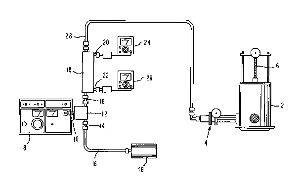
The figure shows a schematic diagram of microwave system
useful to practice the present invention. The workpiece is
placed in microwave cavity 2 wherein the workpiece is
exposed to microwaves by an antennae which is within the
cavity 2. The antenna is controlled by antennae control
means 4. The tuning of the microwave cavity is controlled by
the antennae and by a ground plate, the position of which is
adjustable by plate adjustment means 6. Microwaves are
provided by microwave supply 8 such as model 42081 of
Conversion Technology Corp. Output 10 of source 8 is fed
into a three port circulator 12, such as Number 2620 of
Ferrite Control Company. The three port circulator 12 has an
output 14 which leads through cable 16, such as a type N
cable into a dummy load 18, such as a NARDA 3668 BN load.
Dummy load 18 is there to dissipate radiation reflected from
the cavity 2 due to impedance mismatch due to the
2098416
Y09-92-068 11
-
misplacement of antennae and the adjustable ground plate.
Output 16 of the three port circulator 12 is fed into
directional coupler 18, such as a NARDA 3043 B directional
coupler. Directional coupler 18 has an output 20 and an
output 22, each of which are fed into a power meter and
sensor, such as Hewlett Packard HP 435, 24 and 26
respectively. One of the power meters 24 and 26 measures the
power output from the microwave supply 8 and the other of
the power meters 24 and 26 measures the reflected power from
the workpiece in cavity 2. Output 28 from directional
coupler 18 provides the microwave power to the antennae
controlled by antennae control means 4.
In addition to burning in semiconductor chips individually
or at wafer level, applicants have discovered that
semiconductor chip packaging substrates, such as printed
circuit boards, and metallized ceramic substrates can also
be burned in using the same technique. In addition,
applicants have discovered that semiconductor chips mounted
onto semiconductor chip packaging substrates can be burned
in simultaneously using the techniques of the present
invention.
The mounted semiconductor chips can be singular, as in
single chip modules or multichip modules. Further, in these
structures, the pins can be (i) all electrically connected,
(ii) only ground and power pins connected - signal pins
electrically isolated or (iii) ground and power pins
electrically grounded. Using these configurations, (i)
thermal cycling can be specifically isolated from burn-in
type mechanisms, (ii) higher microwave power levels can be
utilized to accelerate heating rates without causing
excessive electrical overload damage to devices -especially
drivers and receivers.
In the case of mounted semiconductor devices, the microwave
power must be controlled below certain threshold limits
where electrical overload of circuits occurs. This results
in damage to the chip in excess of normal failures
(accelerated or not) and is undesirable. Therefore, there is
- 2098~16
YO9-92-068 12
a process window for mounted chips within which accelerated burn in occurs.
The devices may be a packaging substrate which contains metAlli7ation pattems selected
from a group consisting of a printed circuit board, a ceramic substrate, a metallized flexible
polymer film, a silicon wafer, a glass-ceramic substrate and a glass.
In addition, applicants have discovered that the leakage current of a junction on a
semiconductor device such as a PN junction or a Schottky barrier diode junction, can be
decreased by the application of microwaves. Applicants have measured the leakage current of
a rectifying junction, such as a PN junction such as the emitter base junction of a bipolar
transistor or the collector base junction of a bipolar transistor or the source to channel junction
of an FET transistor or the drain to channel junction of a FET transistor. These junctions have
a specific measured leakage current before exposure to microwaves. When such devices are
exposed to mi~ w~v~ radiation, such as between frequency of about 100 MHz to about 300
GHz, preferably from about 2GHz to about 45 GHz, at a power level from about 100 watts to
about 600 watts, for a time of from about 15 seconds to about 15 minutes, it is found that there
is a decrease in the leakage current. Applicants have found that this leakage current reduction
occurs when fully processed semiconductor chips having substantially fully crystallized or
recrystallized semiconductor material and having one or more levels of metallization thereon
are exposed to microwaves as described herein.
When a bias is applied across a bipolar transistor, a current is formed across the emitter-
base and base collector junctions. This has a well known relationship in ideal transistors.
However, in real cases there are deviations at both the high and low applied voltage regions in
both the forward and reverse bias modes. At high applied voltage saturation occurs while at low
voltage, the current flow is higher than predicted by the ideal relationship. This current
enhancement is due to impurities, imperfections, etc. This current is referred to as a leakage
current.
Quite surprisingly, applicants have discovered that when a fully processed semiconductor
chip having metallization patterns thereon having substantially fully annealed or
2098416
Y09-92-068 13
crystallized semiconducting material is exposed to microwave
radiation, the leakage current of rectifying junctions such
as PN junctions and Schottky junctions is reduced as
compared to the unexposed junctions.
The leakage current limits the performance and yield of a
chip having a plurality of transistors since the gain from
each transistor may be different. This creates device and
circuit tracking problems within the chip as the gain from
two devices may not be the same. Hence, it is difficult to
match the performance of these devices across the wafer
resulting in the yield or performance being degraded as a
result of poor quality transistors. In DRAMS, the leakage
current limits the refresh time of the memory cells. As the
leakage current decreases, the refresh time becomes longer,
resulting in lower power consumption and reduced heat
dissipation.
The cause of leakage current can be surface states, defects,
etc., which, under stress could prove to be a reliability
concern.
To ensure that the metallurgy of a wafer containing a
plurality of semiconductor chips was not deleteriously
affected by microwave radiation, the heating cycle and
residual oxygen during the anneal cycle and to enable the
use of an IR pyrometer to measure the wafer surface
temperature, a thin film of polyimide was applied as an
encapsulant to the active surface of the wafer. The
polyimide film is not necessary to reduce the leakage
current.
After five cycles, wherein each cycle consisting of linear
ramp to 310C in 3 minutes and hold for one minute, the
polyimide encapsulant was removed and the devices tested.
In all but one case, the leakage current was observed to be
substantially reduced to 50% of the value before microwave
exposure for the lowest applied voltage. In the one case in
which the decrease was not observed, the leakage current was
similar to the values obtained after the remaining devices
2098416
Y09-92-068 14
were exposed to the microwave radiation. These results are
shown in the Table below wherein leakage current before and
after microwave cycling are shown for each device tested for
two different sized devices. The reductions measured are
significant and real. The results observed are the same for
both size devices.
TABLE
LEAKAGE CURRENT (IN pA) IN TRANSISTORS - 0 5 VOLTS
ite Number Before Microwave After 5 cycles of microwave
Exposure exposure
2.45GHz 300 Watts for 45 min.
each cycle
1.5 x 1.5~m2 Initial collector Current Collector current after exposure
1 41 19
2 28.5 49
3 28 18
4 29.5 18
31.5 16.5
6 34.5 19.5
0.5 x 0.5 ~m2
SITE Ic Init~al IC After Microwave
1 36 10
2 6 7.5
3 31.5 8.5
4 107.5 10
7 5.5
6 13.5 11
2098~16
Y09-92-068 15
Microwave exposure can also be used to accelerate defects
associated with temperature excursions alone, in chips,
wafers, packaging substrates and modules having chips
mounted onto substrates. Silicon chips are commonly mounted
onto ceramic substrates, polymeric substrates, printed
circuit boards in a flip-chip-configuration with solder
mounds, or solder bumps, commonly referred to as C4s,
electrically interconnecting chips pads and substrate pads.
The thermal coefficient of expansion mismatch between the
chip and substrate can stress the C4 joint. Microwaves can
be used to heat up the assembly of chip and substrate to
accelerate defects in the C4s. The assembly is placed in a
chamber and exposed to microwave radiation using the
techniques and apparatus described herein above. A single
mode cavity is preferred. The temperature of the assembly is
monitored, for example using a pyrometer. The microwave
radiation is discontinued when the desired temperature is
reached. The contents of the chamber are cooled and the
process is repeated up to 100 times. The microwave radiation
can be between 100 MHz and 300 GHz, 50 watts and 600 watts
for from 15 seconds to 15 minutes. For example, eight inch
wafers were moved from room temperature (about 30C) to 200
in 20 seconds, the power was shut off and the wafer was
permitted to cool to room temperature before repeating the
cycle. For example, a module having a chip mounted onto a
substrate was cooled to 10C and microwave heated to 100C
in 20 seconds; the power was shut off and allowed to cool to
room temperature.
The procedure works equally well for chips that are wire
bonded to substrates or lead frames, however, the thermal
cycle failure is not as important in this configuration.
In summary, the present invention is a method of exposing an
electronic device to microwave radiation to burn-in the
device, to electrically stress the device, to thermally
stress the device and to reduce rectifying junction leakage
current in junctions fabricated in substantially fully
crystallized semiconducting material.
Y09-92-068 ~6098416
It is to be understood that the above described embodiments
are simply illustrative of the principles of the invention.
Various other modifications and changes may be devices by
those of skill in the art which will embody the principles
of the invention and fall within the spirit and scope
thereof.