Note : Les descriptions sont présentées dans la langue officielle dans laquelle elles ont été soumises.
20g~
VECTOR PROCESSING DEVICE
BACKGROUNDS OF THE INVENTION
FIELD OF THE INVENTION
The present invention relates to a vector
processing device.
DESCRIPTION OF THE PRIOR ART
A conventional vector processing device processes
list vector instructions in IF statements using masked
vector operations and vector compress and vector expand
instructions, because it is not provided with any means
for masked list vector processing.
Fig. 7 illustrates the vector compress instruction.
The vector data A (al, a2, a3, a4 and a5) are checked
against the mask bits M (1, O, 1, O, 1~ indicated at the
vector control register. From the data A, the elements
at the positions where the mask bit is "1" are picked
up. Such picked up elements replaces the elements in
the vector data B (bl, b2, b3, b4, b5) from the first
end. For the remaining positions of the vector
register, the original elements of the vector data B are
left. Thus, the data B' (al, a3, a5, b4, b5) are
generated. Such vector compress instruction is
hereinafter referred to as a VCP instruction. ~
Fig. 8 illustrate the vector expand instruction.
The elements in the vector data B (bl, b2, b3, b4, b5)
are replaced or left depending on the mask bit M (1, O,
-
209~
--2--
1, 0, 1) at the vector control register. For the
positions where the mask bit is "1", the applicable
element in the vector data A (al, a2, a3, a4, a5)
replaces the element in the data B; when it is "0", the
corresponding element in the data B is left as it is.
Thus, the data B1 (al, b2, a2, b4 and a3) is generated.
Such vector expand instruction is hereinafter referred
to as a VEX instruction.
Fig. 9 shows a configuration example of such a
conventional vector processing device. In the figure,
vector registers 92-1 to 92-8 and a vector control
register 93 are connected to operation devices 94-1 to
94-4 via a crossbar 95. The results obtained at the
operation devices 94-1 to 94-4 can be stored in any of
the vector registers 92-1 to 92-8. In masked operation,
the mask data stored at the vector control register 93
controls whether or not to store an operation result to
a vector register. More specifically, the operation
result is not stored to the element for which the mask
data in the vector control register 93 is "0" and is
stored to the element for which the mask data is "1".
The vector registers 92-1 to 92-8 send data to and
receive data from a main storage 97 via a main storage
controller 96.
Suppose a conditional expression (IF statement) as
follows;
2ag~ 4
D0 10 I = 1, N
IF (M( I).EQ.0)
THEN
X(I) = A(B(I))+C(D(I))
ELSE
X(I)=1
10 CONTINUE
Such an expression may be generally processed by masked
operations for all vector elements (hereinafter referred
to as VL) or by utilizing VCP and VEX instructions with
limiting the processed elements to those for which the
condition is true.
Referring first to the flowchart of Fig. 10, the
method to sub~ect all vector elements (VL) to the masked
operation will be described below with showing the
register contents.
Firstly, a comparison instruction causes comparison
of M( I ) and 0. For a mask generation instruction, the
comparison condition can be specified in the operation
code. This instruction stores "1" when the condition is
true and "0" when it is not true to the vector control
register 93. It is supposed here that the mask data are
(1, 1, 0, 1, 0, 1, 1, 0, ...). Then, ~(I) (bl, b2, b3,
b4, ...) and D(I) (dl, d2, d3, d4 ....) are loaded from
the main storage 97 to the vector registers 92-1 and
92-2.
'' -
2~g~7 l
--4--
The data in the vector registers 92-1 and 92-2 are
read and sent to the main storage controller 96 and then
the main storage 97 is accessed with using B(I) and D(I)
as the address data. Via the main storage controller
96, the data A(B(I))(al, a2, a3, a4 ...) and C(D(I))(cl,
c2, c3, c4 ...) are loaded to the vector registers 92-3
and 92-4. Such processing where the main storage is
accessed using the vector data as addresses for vector
data loading is called the list vector loading.
The data in the vector registers 92-3 and 92-4 are
read out and input to the operation device 94-1 for
processing. Among the results, only those for the
elements having "1" as the mask data are stored to the
vector register 92-5.
Next, a mask reverse instruction is issued so as to
reverse the bits in the vector control register 93 (M'
(O, O, 1, O, 1, O, O, 1 ...)). The elements in the
vector register 92-5 corresponding to "1" in such mask
data are replaced with "1". Then, the contents of the
2~ vector register 12-5 are stored to the main storage 97.
This method is advantageous because it eliminates
the need of auxiliary operations using VCP and VEX
instruction. However, it has a drawback that all vector
elements must be processed even when the rate of "true"
is low.
Next, referring to the flowchart of Fig. 11, the
2~98674
--5--
other method where the elements for which the condition
is true only are processed with utilizing VCP and VEX
instructions, with showing the register contents.
Firstly, a comparison instruction causes comparison
of M(I) and 0, and a mask generation instruction stores
the mask data to the vector control register 93. The
mask data are supposed here to be (1, 1, 0, 1, 0, 1, 1,
0,....). The data B(I) and D(I) are loaded from the
main storage 97 to the vector registers 92-1 and 92-2.
A VCP instruction compresses the data B(I) and D(I) in
the vector registers 92-1 and 92-2 according to the
contents in the vector control register 93 so as to
generate the data B'(I) (bl, b2, b4, b6, b7 ...) and
D'(I) (cl, c2, c4, c6, c7 ...), which are stored to the
vector registers 92-3 and 92-4.
Here, the bits having "1" in the data at the vector
control register 93 are counted (PCNT instruction), and
the counted value is used as the vector processing
element number (VL': VL'<VL). Thereafter, VL' is used
for processing until VL is reset. Then, the data in the
vector registers 92-3 and 92-4 are read out and sent to
the main storage controller 96 and the main storage 97
is accessed with using B'(I) and D'(I) as addresses.
Via the main storage controller 96, the data A(B(I))(al,
a2, a4, a6, a7) and C(D(I))(cl, c2, c4, c6, c7 .. ) are
loaded to the vector registers 92-5 and 92-6. The data
2~9S~7 ~
in the vector registers 92-5 and 92-6 are read out and
input to the operation device (adder) 94-1 for
processing. The operation results are stored to the
vector register 92-7. Then, the VL is reset to the
original value and the data in the vector register 92-7
are expanded by a VEX instruction, and the results are
stored to the vector register 92-8.
Next, a mask reverse instruction is issued so as to
reverse the bits in the vector control register 93 (M'
(0, 0, 1, 0, 1, 0, 0, 1 ... )). The positions in the
vector register 92-8 corresponding to "1" in such mask
data are replaced with "1". Then, the contents in the
vector register 92-8 are stored to the main storage 97.
This method requires shorter operation time when
the rate of "true" is low because processed elements are
limited to those for which the condition is "true" in
the IF statement. It requires, however, auxiliary
operations such as VCP, VEX and PCNT instructions, which
take much time when the rate of "true" is high.
Suppose now a conditional expression as follows:
DO 10 I - 1, N
IF (M(I). EQ. 0) GO TO 10
X (C(I)) = A(I) + B(I)
10 CONTINUE
Conventionally, such an expression is processed by
utilizing VCP and VEX instructions with limlting the
209&~4
processed elements to those for which the condition is
true. Referring to the flowchart of Fig. 12, this
method is described below with showing the register
contents.
Firstly, a comparison instruction causes comparison
of M(I) and 0, and a mask generation instruction stores
the mask data to the vector control register 93. The
mask data are supposed here to be (1, 1, 0, 1, 0, 1, 1,
0,....). The data A(I), B(I) and C(I) are loaded from
the main storage 97 to the vector registers 92-1, 92-2
and 92-3. The data in the vector registers 92-1 and
92-2 are read out and input to the operation device
(adder) 94-1 for processing. The results are stored to
the vector register 92-4, only for the positions for
which the mask data is "1".
Then a VCP instruction compresses the addition
results (store data) in the vector register 92-4 and and
the address data C (I) in the vector register 92-3
according to the contents in the vector control register
93 and stores the results to the vector registers 92-5
and 92-6. Here, the bits having "1" in the data at the
vector control register 93 are counted ~PCNT
instruction), and the counted value is used as the
vector processing element number (VL'). Thereafter, VL'
is used for processing until VL is reset. Then, the
store data stored in the vector register 92-5 and the
~98~7~
address data (C'(I)) stored in the vector register 92-6
are read out and sent to the main storage controller 96.
The store data are stored to the vector storage 97 using
the data C'(I) as the addresses. An advantage of this
method is that the vector elements to be processed are
limited to those for which the condition is true and no
other elements are processed. However, the need of
auxiliary operations such as VCP and PCNT instructions
results in a lengthy operation.
As described above, a conventional vector
processing device has drawbacks concerning processing of
list vectors in conditional expressions. When it
processes all vector elements by masked operation, it
eliminates the need of auxiliary operations, but has to
perform many unnecessary operations because all vector
elements are processed even when the rate of "true" is
low.
When the vector processing device adopts the other
method where the true elements only are processed with
using VCP and VEX instructions, the operation time
becomes shorter when the rate of "true" is low because
the true vector elements only are processed, but it
requires auxiliary operations such as VCP and VEX
instructions.
Besides, in order to take the maximum advantage of
a vector processing device, it is necessary to adopt the
2~:g8~ ~
most suitable method for the program. For this purpose,
a conventional device requires a compiler which examines
the rate of "true" and other information for the
conditional expression in the program so as to select
the suitable one from the two methods above.
SUMMARY OF THE INVENTION
An ob;ect of the present invention is to provide a
vector processing device which eliminates the need of
auxiliary operations such as VCP and VEX instructions
and PCNT instructions and reduces the number of accesses
to the main storage and thereby improves the speed of IF
statement processing.
According to a preferred embodiment of the present
invention to attain the above object, a vector
processing device comprises a vector processor further
containing more than one vector register, operation
means for vector operation and a vector control register
to store the mask information indicating the
effectiveness of the vector data, a storage to store the
vector data, and a storage controller to control
accessing to the storage, and the storage controller
further comprises a store direction means to generate a
signal to direct whether or not to store the vector data
to be stored from the vector processor to the storage
according to the mask information and a means to store
2o9~6~ ~
--10--
the data obtained by access to the storage to the vector
register according to the mask information.
According to a still preferred embodiment of the
present invention the storage controller comprises an
address information registration means to store the
address data for access to the storage stored in the
vector register and a mask registration means to hold
the contents of the vector control register. Further,
the storage controller comprises a load data storage
means to temporarily store the data obtained by access
to the storage and a store data storage means to
temporarily store the data to be stored to the storage.
According to a further preferred embodiment of the
present invention, the store direction means generates a
signal to direct storing of the vector data at the
positions where the mask information is "1" to the
storage and the data storage means stores the data for
which the mask information is "1" to the vector register
and does not store those for which the mask information
is "0" to the vector register.
According to another preferred embodiment of the
present invention to attain the above object, a vector
processing device comprises a vector processor further
provided with more than one vector register, operation
means for vector operations and a vector control
register to store the mask information indicating the
~9~674
--11--
effectiveness of the vector data, a storage to store the
vector data, and a storage controller to control
accessing to the storage and the storage controller
further comprises an address data selection means to
select the address data to access to the storage stored
at the vector register according to the mask information
and a data storage means to store the data obtained by
accessing to the storage using the selected address data
to the vector register according to the mask
information.
According to a still preferred embodiment, the
address data selection means comprises an address
information registration means to store the address data
for access to the storage stored in the vector register,
a mask registration means to keep the mask information
for the vector control register and an access control
means to select the address data from the address
information registration means based on the mask
information registered to the mask registration means
and the data storage means further comprises a load data
storage means to temporarily store the vector data
obtained by access to the storage using the address data
selected by the access control means and a load data
expansion means which uses the data held at the load
data storage means to expand the load data according to
the mask information stored to the mask registration
6 ~ ~
-12-
means so as to store them to the vector register. Further, the
storage controller comprises an access information
registration means further comprlslng an address information
registration means to store the address data for access to the
storage stored in the vector register and a store data storage
means which keeps the vector data to be stored to the storage,
and an access control means to obtain the store data to be
stored to the storage according to the mask informatlon and
the storing address on the storage from the access informatlon
registration means.
According to a still preferred embodiment, the
access control means accesses the storage at the addresses in
the address lnformatlon reglstratlon means for which the mask
lnformatlon ls "1", and does not access the storage at the
addresses of the address information registration means for
whlch the mask lnformation is "0". Further, the load data
expansion means stores the load data for the elements of the
vector register for which the mask information is "1" and
stores an arbitrary value for the elements of the vector
reglster for which the mask informatlon ls "0".
In accordance with the present lnvention, there ls
provided a vector processlng devlce comprlslng:
a vector processor comprlslng more than one vector
reglster, operatlon means for vector operatlon, and a vector
control reglster to store mask informatlon for the vector
data,
a vector data storage for storlng said vector data, and
74660-7
~j
-12a-
a storage controller for controlllng accessing to sald
vector data storage based on a masked 11st vector lnstructlon,
sald storage controller further comprlslng
an address lnformatlon registratlon means for storing
address for access to said vector data storage stored ln said
vector register, and
a mask registration means for holding sald mask
lnformatlon sent from sald vector control reglster,
a request generation means for generating a request
slgnal to dlrect whether or not to store the vector data to be
stored from sald vector processor to said vector data storage
according to sald mask lnformation,
a load data storage means for temporarily storlng the
vector data read out by access to sald vector data storage
means, and
a store data storage means for temporarlly storlng the
vector data to be stored ln sald vector data storage means
whereln for processlng of a masked 11st vector store
lnstructlon, sald request generatlon means generates sald
request slgnal to direct storing of the vector data at
posltlons for whlch sald mask lnformation is "1" in said
vector data storage and does not generate sald request slgnal
when sald mask lnformatlon ls "0", and sald storage controller
stores the vector data ln sald vector data storage means based
on sald request signal and address stored in sald address
informatlon reglstration means,
for processlng of a masked list vector load instructlon,
74660-7
-12b-
said storage controller reads out vector data for which said
mask lnformatlon is "1" from sald vector data storage based on
address stored in sald address lnformatlon reglstratlon means
and stores the vector data ln sald vector reglster, and does
not store vector data for which said mask information is "0"
in said vector reglster to thereby leave the vector data
originally existing in sald vector register.
In accordance wlth another aspect of the inventlon,
there ls provided a vector processing device comprislng:
a vector processor further comprising more than one
vector register, an operation means for vector operations and
a vector control register to store the mask information for
the vector data,
a vector data storage for storing said vector data, and
a storage controller for controlling accesslng to sald
vector data storage based on a masked 11st vector instruction,
said storage controller further comprlslng
an address data selectlon means for selectlng the address
to access to said vector data storage stored at sald vector
~0 reglster accordlng to sald mask lnformation, and
a data storing means for storlng the vector data obtalned
by accesslng to sald vector data storage uslng sald selected
address to sald vector reglster accordlng to sald mask
lnformatlon,
whereln sald address data selectlon means comprlses
an access lnformatlon reglstratlon means for storlng the
address for access to sald vector data storage stored ln said
74660-7
-12c-
vector reglster,
a mask registratlon means for holding the mask
lnformation for sald vector control reglster, and
an access control means for selecting the address from
sald address information reglstration means based on said mask
information registered to said mask registration means,
said data storing means further comprises
a load data storage means for temporarily storing the
vector data obtained by access to said storage uslng the
~0 address data selected by said access control means, and
a load data expansion means for expanding the load vector
data held at said load data storage means according to said
mask information stored ln said mask registration means and
for storing the expanded load vector data in said vector
register.
Other obiects, characteristics and effects of the
present invention will be clarified in the detailed
description below.
74660-7
209&~7~
-13-
BRIEF DESCRIPTION OF THE DRAWINGS
Fig. 1 is a block diagram to show the configuration
of a vector processing device according to a first
embodiment of the present invention;
Fig. 2 is a block diagram to show the configuration
of a vector processing device according to a second
embodiment of the present invention;
Fig. 3 is an explanatory view of the masked list
vector loading by a vector processing device according
to the second embodiment;
Fig. 4 is an explanatory view of the masked list
vector storing by a vector processing device according
to the second embodiment;
Fig. 5 is a flowchart to illustrate the processing
of an IF statement including list vector loading by a
vector processing device of the present invention;
Fig. 6 is a flowchart to illustrate the processing
of an IF statement including list vector storing by a
vector processing device of the present invention;
Fig. 7 is an explanatory view to illustrate the
operation caused by a vector compress instruction;
Fig. 8 is an explanatory view to illustrate the
operation caused by a vector expand instruction;
Fig. 9 is a configuration example of a conventional
vector processing device;
Fig. 10 is a flowchart to illustrate a first
~g8~
-14-
conventional method of processing for an IF statement
including list vector loading;
Fig. 11 is a flowchart to illustrate a second
conventional method of processing for an IF statement
including list vector loading; and
Fig. 12 is a flowchart to illustrate a conventional
method of processing for an IF statement including list
vector storing.
DESCRIPTION OF THE PREFERRED EMBODIMENT
Referring to the attached figures, preferred
embodiments of the present invention will be described
in detail below.
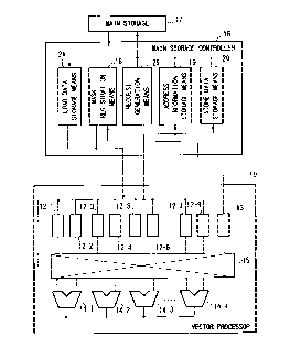
Fig. 1 is a block diagram to show the configuration
of a vector processing device according to a preferred
embodiment of the present invention. A vector processor
10 comprises more than one vector register (vector
registers 12-1 to 12-8), a vector control register 13, a
plurality of operation devices (14-1 to 14-4) and a
crossbar 15. The vector registers 12-1 to 12-8 and the
vector control register 13 are connected to the
operation devices 14-1 to 14-4 via the crossbar 15.
The results obtained by the operation devices 14-1
to 14-4 can be stored to any of the vector registers
12-1 to 12-8. Further, in masked operation, mask data
stored in the vector control register 13 controls
2~9867~
-15-
whether or not to store the elements of the operation
results to the vector registers 12-1 to 12-8. The
vector registers 12-1 to 12-8 send data to and receive
data from the main storage 17 via the main storage
controller 16 (to be described below).
The main storage controller 16 comprises a mask
registration means 18, an address information
registration means 19, a load data storage means 21, a
store data storage means 20 and a request generation
means 25. The address information registration means 19
keeps the addresses to access the main storage 17 sent
from the vector registers 12-1 to 12-8 and the store
data storage means 20 keeps the vector data to be stored
to the main storage 17.
The load data storage means 21 temporarily keeps
the vector data obtained by accessing the main storage
17. The mask registration means 18 keeps the mask data
sent from the vector control register 13. Such mask
data are sent to the vector processor 10 together with
the load data stored in the load data storage means 21.
The request generation means 25 converts the mask data
stored in the mask registration means 18 into request
signals. The main storage 17 stores the store data in
the store data storage means 20, only for the elements
for which the request signals are received.
For processing of a masked list vector load
20~g~
-16-
instruction, the main storage 17 is accessed at the
addresses kept at the address information registration
means 19. The data obtained by such accessing are
temporarily stored in the load data storage means 21 and
sent to the vector processor 10 together with the mask
data in the mask registration means 18. For the
elements of the vector register at the positions for
which the mask data sent from the main storage
controller 16 is "1", the load data sent from the main
storage controller 16 are stored. For the vector
register elements at the positions for which the mask
data is "0", the load data sent from the main storage
controller 16 are not stored and the data originally
existing in the vector register are left.
For processing of a masked list vector store
instruction, when the mask data stored in the mask
registration means 18 is "1", the request generation
means 25 converts such data into a request signal, which
directs writing of data to the main storage 17. When
the mask data is "0", it does not convert the data into
a request signal. Together with the data after
conversion to a request signal, address and store data
are sent to the main storage 17. The main storage 17
stores the store data when it recognizes the request
signal. In other words, the store data for the
positions where the mask data in the mask registration
2 ~
-17-
means 18 is "1" are stored to the main storage 17, but
those for the positions where the mask data is "0" are
not stored to the main storage 17.
Fig. 2 shows the conflguration of a vector
processing device according to a second embodiment of
the present invention. In the figure, a vector
processor 10 has the same configuration as the first
embodiment shown in Fig. 1.
A main storage controller 16 comprises a mask
registration means 18, a memory access information
registration means 24, a load data storage means 21, a
memory access control means 22, a load data expansion
means 23. The memory access information registration
means 24 comprises an address information registration
means 19 to store the addresses for access to the main
storage 17 and a store data storage means 20 to store
the data to be stored to the main storage 17.
The mask registration means 18 keeps the mask data
sent from the vector control register 13 in the vector
processor 10 and the memory access control means 22
selects the information for access to the main storage
17 from the memory access information registration mean
24 according to the mask data contents stored in the
mask registration means 18.
For processing of a list vector load instruction,
the memory access control means 22 controls the device
2'0'~ 7 ~
-18-
so that it accesses the main storage 17 at the
addresses, among those kept at the address information
registration means 19, corresponding to the positions
for which the mask data stored in the mask registration
means 18 is "1" and does not access the main storage 17
at the addresses corresponding to the positions for
which the mask data is "0".
The load data obtained by such access to the main
storage 17 are temporarily kept at the load data storage
means 21. The load data expansion means 23 expands the
load data in the load data storage means 21 according to
the same principle as the VEX instruction.
Specifically, it expands the load data for the positions
where the mask data is "1" and stores an arbitrary value
for the positions where the mask data is "0".
The values in the above step need not to be
assured. When the data generated by the load data
expansion means 23 are sent to the vector processor 10
to be stored to an arbitrary vector register, the mask
data at the mask registration means 18 are together sent
to the vector processor 10. Thus, the data sent from
the main storage 16 are stored for the vector register
elements at the positions for which the mask data is
"1". For the positions where the mask data is "0", the
data originally stored in the vector register are left
and the data sent from the main storage controller 16
2~67ll
--19--
are not stored.
Referring now to the data flow in Fig. 3, the
operation for a masked list vector load instruction at
the vector processing device according to the second
embodiment is described.
Suppose here that the vector register 12-1 keeps
the address data A (al, a2, a3 .... alO) for access to
the main storage 17, the vector register 12-2 keeps X
(xl, x2, x3 ... , xlO) and the vector control register
13 keeps the mask data (1, 1, O, 1, O, 1, 1, O, O, 1).
When a masked list vector load instruction is
issued, the vector processor 10 sends the address data
and mask data to the main storage controller 16. The
mask data (1, 1, O, 1, O, 1, 1, O, O, 1) are stored to
the mask registration means 18 and the address data (al,
a2, a3, .... alO) are stored to the address information
registration means 19. The memory access control means
22 sends the addresses for the positions where the mask
data is "1" in the mask registration means 18, i.e. (al,
a2, a4, a6, a7, alO), to the main storage 17. The main
storage 17, upon receipt of these addresses, sends the
data corresponding to these addresses (al, a2, a4, a6,
a7, alO) to the load data storage means 11. Suppose the
data here are B(bl, b2, b4, b6, b7, blO).
The load data expansion means 23 stores the data
B(bl, b2, b4, b6, b7, blO) to the positions where the
"~ -
20~36~ ~
-20-
mask data in the mask registration means 18 is "1"
(first, second, fourth, sixth, seventh and tenth
elements) and stores an arbitrary value (*) at the
positions where the mask data is "O" (third, fifth,
eighth and ninth elements). Thus, the data B'(bl, b2,
*, b4, *, b6, b7, *, *, blO) are generated. Then the
data B' are sent to the vector processor 10 so as to be
stored in the vector register 12-2.
When the data is stored to the vector register
12-2, the data B' elements are stored for the positions
for which the mask data in the vector control register
13 is "1" (first, second, fourth, sixth, seventh and
tenth elements). For the positions where the mask data
is "O" (third, fifth, eighth and ninth elements), the
data X elements (x3, x5, x8, x9) originally stored in
the vector register 12-2 are kept. As a result, the
vector register 12-2 has the vector data X'(bl, b2, x3,
b4, x5, b6, b7, x8, x9, blO) after the masked list
vector load instruction.
For processing of a list vector store instruction,
the store data elements in the store data storage means
20 corresponding to the positions for which the mask
data in the mask registration means 18 is "1" are sent
to the main storage 17 together with the addresses
corresponding to such elements in the address
information registration means 19. Thus, the store data
2~98~
-21-
are stored to the main storage 17 with avoiding data
replacement for the positions where the mask data is "O"
in the main storage 17.
Referring now to the data flow in Fig. 4, the
operation for a masked list vector store instruction at
the vector processing device according to the second
embodiment is described. Suppose here that the vector
register 12-1 keeps the address data A (al, a2, a3 ....
alO) for access to the main storage 17, the vector
register 12-2 keeps B (bl, b2, b3 .... , blO) to be
stored to the main storage 17 and the vector control
register 13 keeps the mask data (1, 1, O, 1, O, 1, 1, O,
O, 1).
When a masked list vector store instruction is
issued, the vector processor 10 sends the address data,
store data and mask data to the main storage controller
16. The mask data (1, 1, O, 1, O, 1, 1, O, O, 1) are
stored to the mask registration means 18, the address
data (al, a2, a3, .... alO) are stored to the address
information registration means 19 and the data (bl, b2,
b3, ... blO) are stored to the store data storage means
20. The memory access control means 22 sends the
address and store data for the positions where the mask
data is "1" in the mask registration means 18, i.e. (al,
a2, a4, a6, a7, alO) and (bl, b2, b4, b6, b7 and blO),
to the main storage 17. The main storage 17 stores the
2093~7~
store data (bl, b2, b~, b6, b7, blO) to the positions
specified by the addresses (al, a2, a4, a6, a7, alO).
Referring to the flowchart and the register
contents shown in Fig. 5, the vector processing device
is now supposed to process, for example, the conditional
expression (IF statement) as follows:
DO 10 I = 1, N
IF (M(I). EQ. O)
THEN
X(I) = A(B(I)) + C(D(I))
ELSE
X(I) = 1
10 CONTINUE
Firstly, a comparison instruction causes comparison
of M(I) and 0. A subsequent mask generation instruction
stores the mask data to the vector control register 13.
Suppose here that the mask data are (1, 1, O, 1, O, 1,
1, O, ...). Then, the data B(I) and D(I) are loaded
from the main storage 17 to the vector registers 12-1
and 12-2.
Next, a masked list vector load instruction causes
the data in the vector registers 12-1 and 12-2 to be
read out and sent to the main storage controller 16, and
at the same time causes the mask data in the vector
control register 13 to be sent to the main storage
controller 16. The main storage controller 16 follows
209~
-23-
the method as described above to load the data
A(B(I))(al, a2, *, a4, *, a6, a7 ...) and (D(I))(cl, c2,
*, c4, *, c6, c7,...) to the elements where the
condition of the IF statement is true (first, second,
fourth, sixth, seventh ... elements) and stores them to
the vector registers 12-3 and 12-4. Then, the data in
the vector registers 12-3 and 12-4 are read out and
input to the adder 14-1 for processing, and the results
are stored to the vector register 12-5. The vector
register 12-5 is supposed to keep the vector data X(Xl,
X2, X3, X4, X5, X6, X7, ...) as the initial values.
Next, a mask reverse instruction reverses the bits
in the vector control register 13 to obtain the data
M'(0, 0, 1, 0, 1, 0, 0, 1). The elements in the vector
register 12-5 for which the mask data is "1" (third,
fifth, eighth .... elements) are replaced with the
immediate value "1". Then, the contents of the vector
register 12-5 are stored to the main storage 17.
The IF statement processing as described above with
the vector processing device according to the first or
second embodiment reduces the number of accesses to the
main storage 17, and at the same time, shortens the data
storing time for the vector registers. Further, such
procedure using a masked list vector loading eliminates
the need of conventional auxiliary operations, which
improves the speed of processing.
2Q~674
-24-
Referring to the flowchart and the register
contents in Fig. 6, another example of processing is
described with supposing an IF statement as follows:
DO 10 I = 1, N
IF (M(I). EQ. O) GO TO 10
X(C(I)) = A(I)+B(I)
10 CONTINUE
Firstly, a comparison instruction causes
comparison of M(I) and 0. A subsequent mask generation
instruction stores the mask data to the vector control
register 13. Suppose here that the mask data are (1, 1,
0, 1, 0, 1, 1, 0, ...). Then, the data A(I), B(I) and
C(I) are loaded from the main storage 17 to the vector
registers lZ-l, 12-2 and 12-3.
Next, the data in the vector registers 12-1 and
12-2 are read out and input to the adder 14-1 for
processing. The operation results are stored to the
vector register 12-4, only for the elements at the
positions where the mask data in the vector control
register 13 is "l" (first, second, fourth, sixth,
seventh .... elements). ~or the elements at the
positions where the mask data is "0" (third, fifth,
eighth .... elements), the initial data of the vector
register 12-4 are left. The resulting data are (al+bl,
a2+b2, *, a4+b4, *, a6+b6, a7+b7, *, .... ). The vector
register 12-5 is supposed to keep the vector data X(X1,
~5~
-25-
X2, X3, X4, X5, X6, X7, ...) as the initial data.
Next, a masked list vector store instruction reads
out the address data and the store data from the vector
registers 12-3 and 12-4 respectively and sends them to
the main storage controller 16. The main storage
controller 16, upon receipt of the address data and the
store data, stores the store data to the main storage 17
only for the elements for which the condition in the IF
statement is true (first, second, fourth, sixth, seventh
... elements).
With the vector processing device according to the
first and the second embodiments, IF statements can be
processed with a reduced number of accesses to the main
storage 17 and in a shorter time for data storing to the
vector registers. Besides, masked list vector storing
eliminates the need of conventional auxiliary
operations, which improves the operation speed.
Thus, a masked list vector loading instruction
during list vector loading for an IF statement
eliminates the need of auxiliary operations. Since the
load data can be obtained by access to the maln storage
only when the condition of the IF statement-is true,
such method further reduces the number of accesses to
the main storage, which improves the speed of
conditional list vector loading. In list vector storing
for an IF statement, a masked vector store instruction
-
20~8674
-26-
eliminates the need of auxiliary operations. Besides,
since the subject data are stored with access to the
main storage only when the condition of the IF statement
is true, the number of accesses to the main storage is
reduced, which improves the speed of storing. This also
eliminates the need of a compiler which changes the
method of processing according to information including
the rate of "true" for the applicable IF statement.
Obviously, various modifications can be made to the
above embodiments. It is intended to cover in the
appended claims all such modifications and variations as
fall within the true spirit and scope of the present
invention.