Note : Les descriptions sont présentées dans la langue officielle dans laquelle elles ont été soumises.
WO 92/12540 PCT/G B91/022i0
:w
G.n ~, ' . ~ : :l ..
1
Semiconductor Device
':his invention relates to a semiconductor device. ylore particuiar_y.
although not exclusively, it relates to such devices which are
heterostructures of narrow bandgap semiconductor materials.
Narrow bsndgap semiconductors such as InSb have useful properties such
as very low electron effective mass, very high electron mobility and
high saturation velocity. These are potentially of great interest for
high speed device applications. Unfortunately it has proved difficult
to overcome the drawbacks of these materials. A prior art three
terminal active device which is a narrow bandgap semiconductor material
heterostructure is described by T Ohashi et al in J Vac Sci Technol B4
622 (1986). It is a thin film depletion mode field effeet transistor
(FET) device, and consists of an InSb film on a GaAs substrate.
::owever, the device of Ohashi et al unfortunately has poor performance,
a high leakage current in particular. It has a dynamic range of only
'7dB, and so its current in an ON state is only about twice (51/2) that
in an OFF state. This exemplifies the difficulty of exploiting the
useful properties of narrow bandgap semiconductors.
European Patent Application No 8530405.1-2203 published as No 0 16'7 305
discloses photodiodes having two or more terminals and formed as
heterostructures of semiconductor materials. There is no disclosure of
field effect transistors or bipolar transistors.
It is an object of the invention to provide an alternative form of
semiconductor device.
The present invention provides a semiconductor device having first.
second snd third semiconducting regions connected in series for current
input, current control and current output respectively and each arranged
to be biased by a respective biasing means, the device incorporating an
WO 92/12540 PCT/GB91/02270
'; : 1 ~,
2
extracting contact arranged to extract minority carriers from the second
region, and the second region being of low doping and having a common
interface with a fourth semiconducting region itself having a common
interface with a fifth samiconducting region, and wherein the fourth
region:
(a) has like majority carrier type to that of the fifth region.
(b) is biasable through the fifth region and is arranged to act as
an excluding contact to exclude minority carriers from at
least parts of the second region adjacent the third region and
thereby to reduce the intrinsic contribution to current
reaching the third region,
(c) has a bandgap sufficiently large to provide a potential energy
barrier to minority carrier flow from the fifth region to the
second region,
(d) has sufficiently high doping to counteract potential barrier
impediment to majority carrier flow from the second region to
the fifth region, and
(e) is less wide than a critical thickness associated with
dislocation formation but sufficiently wide to inhibit
tunnelling of minority carriers from the fifth region to
the second region.
The expressions "extracting contact" and "excluding contact" are known in
the art of semiconductor devices. The former relates to a junction which
gathers minority carriers which diffuse to it, and the latter a junction
which accepts majority Carriers but does not supply minority carriers.
The invention provides the advantage that it makes possible the
production of devices not produced in the prior art and the attainment
of improved dynamic range; an enhancement mode field effect transistor
embodiment of the invention formed from narrow bandgap semiconductor
material has exhibited a dynamic range of 23d8~ Such an FET device has
WO 92/12540 PCT/G B91/02270
~Ll ~ ~; ,j
not been made in the prior art. Moreover, this embodiment has a dynamic
range which is a l6dB improvement over a prior art depletion mode device
formed from narrow bandgap semiconductor material. In such an
embodiment of the invention, the first, second and third regions are
source, gate and drain regions respectively, and the first and third
regions are of like majority carrier type opposite to that of the
second, fourth and fifth regions.
The invention may alternately be arranged as a depletion mode field
effect transistor, in which case the first. second and third regions are
source, gate and drain regions of like majority carrier type opposite to
that of the fourth and fifth regions.
The second region may be a layer having first and second sides separated
by the layer thickness, the first and third regions being connected to
the first side of the second region, the fourth region being connected
to the second side of the second region and the fifth region being
connected to a side of the fourth region remote from the first, second
and ,third regions. The fourth region may be connected to the second
region over an area at least as extensive and correspondingly located as
those parts of the second region ad3acent and between the first and
third regions, the fourth region being arranged to provide minority
carrier exclusion over most or all of the second region.
A device of the invention may have constituent semiconductor materials
with narrow bandgaps, ie bandgaps less than 0.5eV.
In a preferred embodiment, the invention is an enhancement mode field
effect transistor having the following constituent regions:
(a) first snd third regions of InSb having an n-type dopant
concentration of at least 2x10¹⁷ atoms/cm3.
WO 92/12540 PCT/G B91/02270
~~ Y.i ~~ A.n
4
(b) a second region of InSb having a p-type dopant concentration of
less than 1x101 atoms/cm3,
(c) a fourth region of Ini.xAlxSb having a p-type dopant
concentration of at least 5x10 1 atoms/cm~, where x is a
compositional parameter in the range 0.01 to 0.~, end
(d) a fifth legion of InSb with a p-type dopant concentration of at
least 5x101 atoms/cm3.
The invention may be formed from a series of layers disposed successively
un a common substrate, the fifth region being a first layer supported by
the substrate, the fourth region being a second layer in contact with the
fifth layer, the second region being a third layer in contact with the
second layer. and the first and third regions being formed from a common
fourth layer in contact with the third layer.
In an alternative embodiment, the invention is a bipolar trsnsi~tor in~.
which the first, second and third regions are emitter, base and collector
regions respectively, and the first and third regions are of like
majority carrier type opposite to that of the second. fourth and fifth
regions. In a preferred version of this embodiment, the second region is
a layer having first and second sides separated by the layer thickness.
the first and third regions are connected respectively to the first and
second sides of the second region, the fourth region is connected on one
side to the first side of the second region and on the other side to the
fifth region. The second region may have a further biasing means
connected to a different part of the second region to that to which the
fourth region is connected: this further biasing means may be biasable
independently of the fourth region and may incorporate semiconducting
regions of like composition to those of the fourth and ,fifth regions.
The further biasing mesas and the fourth region may be annular and
disposed around the first region.
A bipolar transistor of the invention may incorporate the following:
WO 92/12540 PCf/GB91/02270
~, ,. ,. .,~ r3 ~i ~~
.:_,. ,.,, ,,
~J ~.' Ci =: 4~
7
(a) first and third regions of InSb having an n-type dopant
concentration of at least 2x101 atoms/cm3,
(b) a second region of InSb having a p-type dopant concentration of
less than 1x101 atoms/cm~,
(c) a fourth region of Inl_xAlxSb having a p-type dopant
concentration of at least 5x101 atomsjcm~, where x is a
compositional parameter in the range 0.01 to 0.~, and
(d) a fifth region of InSb with a p-type dopant concentration of at
least 5x101 atoms/cm3.
A device of the invention may incorporate a fourth region of
seiconductor bandgap at least (3kT/q) Volts, preferably (5kT/q) Volts,
wider than that of either the second region or the fifth region, where k
is the Holtzmann constant, T the absolute temperature and q the
electronic charge.
In order that the invention might be more fully understood, embodiments
thereof will now be described. by way of example only, with reference to
the accompanying drawings, in which:-
Figure 1 schematically illustrates a semiconductor heterostructure;
Figure 2 schematically illustrates a semiconductor heterostructure
in the form of an extracting diode;
Figure 3 graphically illustrates variation of conduction band and
valence band edge energies along the Figure 2 diode;
Figure 4 graphically illustrates variation of the product of zero bias
resistance and area with temperature for diodes respectively
with and without minority carrier barrier layers;
WO 92/12540 PCT/G B91/02270
6
Figure 5 graphically illustrates the reverse bias current-voltage and
differential conductance-voltage characteristics, at 70°C, of
an InSb diode of the invention;
Figure 6 schematically illustrates a semiconductor heterostructure
grown to produce a MISFET of the invention;
Figure j schematically illustrates stages in the fabrication of a
MISFET of the invention from the heterostructure of Figure 6;
Figure 8 graphically illustrates output characteristics of a MISFET of
the invention;
Figure 9 is a schematic cross-sectional view of a bipolar transistor
of the invention; and
Figure 10 is a schematic cross-sectional view of a further embodiment
of a bipolar transistor of the invention.
Referring now to Figure 1, there is shown schematically a semiconductor
multilayer heterostsucture 10 suitable for constructing devices of the
invention. The heterostructure 10 consists of indium antimonide (InSb)
and indium aluminium antimonide (Inl_xAlxSb) alloys. It has four
regions of semiconductor material as follows: a heavily doped narrow
bandgap p-type (p') region 12, a relatively wide bandgap heavily doped
narrow bandgap p-type (R') region 14, a lightly doped p-type (p') region
16 and a heavily doped narrow bandgap n-type (n') region 18. In this
specification a superscript minus (-) or plus (~) indicates light or
heavy doping respectively, the absence of a superscript indicates an
intermediate doping level. The bar (_) subscript indicates material of
wide bandgap relative to the bandgap of material denoted without the
bsr. Adjacent pairs of the regions 12, 14. 16 and 18 have respective
intermediate regions indicated by lines 20. 22 and 24, and which arP
p'I2'. it'p~ and p'n' junctions respectively. Regions 20 and 22 are
heterojunctions and region 24 is a homojunction, and all three are
referred to as junctions hereinafter.
WO 92/12540 s " ,~, ,,~ r~ .~ ~'p PCT/GB91/02270
~J ii ~... ~.i ,J i_ ll
The heterostructure 10 is grown in a VG V80H MHE system on a p-type
(cadmium doped to 3x101~'cm-3) (001) InSb substrate 26. Adjacent to the
substrate 26 is a buffer and temperature ramp region 28 grown whilst the
MBE system was being set up correctly to grow the heterostructure 10.
The growth temperature was approximately 420°C and the growth rate
was
0.5micronshr'1. Mesa diode fabrication is performed using standard
photolithographic techniques, on the heterostructure 10, to
define chemically etched structures.
The p', p' and n' regions 12. 16, 18 consist of InSb cf widths
2.15microns. 3.15microns. and 3.Omicrons respectively. InSb has a
bandgap of 0.18eV at room temperature. The p' region 14 consists of
in~,9Alo.lSb of width 0.02microns. Ino.9Alo.iSb has a bandgap at room
temperature of 0.36eV, twice the bandgap of InSb. Dopants are silicon
(Si) for n-type and beryllium (Be) for p-type. Doping in regions 12 and
14 is 5x10¹⁸atomscm'3, in region 16 is 1x10¹⁵atomscm'3 and in region 18
is 1x10¹⁸atomscm'3.
Referring now to Figure 2, there is shown schematically a semiconductor
device 30 in the form of a diode. The diode 30 will be described in
order to clarify the roles of excluding contacts, extracting contacts
and potential barriers employed in devices of the invention. Parts
common to Figure 1 are like referenced. The diode 30 is composed of
regions 12, 14. 16 and 18 with intervening.junctions 20, 22 and 24 as
described with reference to Figure 1. As will be described later, the
~'p- junction 22 forms an excluding contact and the p'n' junction 24
forms an extracting contact. Electrodes to the diode 30 are provided at
32 and 34 for bias voltage application.
Region 12 provides a narrow bandgap region to which the electrode 32 may
be attac:eu sad tha width of this region is not critical. In this
embodiment region 12 has width of 2.15microns between electrode 32 and
junction 22. Region 14 must have sufficient width such that minority
carriers are substantially prevented From tunnelling from region 12 to
region 16, that is wider than about 2nm. This is discussed is more
detail later. However, region 14 must also 'be narrower than the
WO 92/12540 PCT/G B91/02270
.. , , ~. ~~ g
C. ',,r ,:: ,.,~ :J _
critical width for strain relief; this critical width is a term of art
for the layer thickness, which, if exceeded, results in the layer
failing to accommodate strain associated with conformity with the
layer's substrate crystal lattice. Layers with widths above the
critical width have dislocations giving rise to unwanted energy states
which conflict with device operation. In Ino.9Alo.lSb, the critical
width is estimated to be 50nm (from a model by J W Matthews and A E
Blakeslee in J Crystal Growth 27, 118 (1975). Region 14 has a width
between junctions 20 and 22 of 20nm, less than half the estimated
critical width. Region 16 should have a thickness between junctions 22
and 24 which is not greater than a minority carrier diffusion length, in
order that the minority carrier exclusion and extraction effects
produced within it by these junctions extend throughout its thickness.
It is also important that there is no source of minority carriers to
region 16, that is no electrical connections through which minority
carriers may be injected into this region. If there were such a source,
exclusion and extraction effects would be nullified.
In the diode 30 region 16 hrs s width betweEn jun:.tior.s 22 and 24 of
3.15microns. Region 18 provides for carrier extraction; its width
should be greater than a minority carrier diffusion length, eg a width
between junction 24 and electrode 34 of 3. Omicrons.
Referring now also. to Figure j, this provides curves 40 and 42
illustrating graphically the variation in conduction and valence band
edge energies. E~ and E~ respectively, along the diode 30, at zero bias.
Chain lines 44, 46 and 48 indicate positions of junctions 20, 22 and 24
respectively. A dashed line 50 indicates the Fermi level through the
diode 30. The g' region 14 produces a potential barrier 52 in the
Conduction band which prevents minority carriers (electrons) from the p'
region 12 entering the p' region 16. In addition, because the bandgap
of the g' region 14 is wider than that of other rAa;~nc, olo._.Tr~n
generation in it by thermal excitation is relatively small. The p'p'
junction 22 therefore forms an excluding contact which excludes
electrons (minority carriers) from reaching the region 16 from its left.
The p' region 14 must, however be sufficiently wide to prevent any
substantial degree of minority carrier transport from region 12 to
WO 92/ 12540 . ~ ~ a , ~ .,~; , s - ~ ~ PCT/GB91 /02270
fa a .~ V v .:.
9
region 16 by quantum mechanical tunnel effect through the potential
barrier 52.
~ne width required for the region 14 is a function of the form of the
potential energy barrier 52 and the carrier effective mass. An
approximate analysis is derived from R A Smith, "Wave Mechanics of
Crystalline Solids" 2nd edition. Chapman and Hall (1969) page 56, for a
rectangular barrier with equal conduction and valence band edge
energies. E~ and E~, on either side of the barrier. Moreover the
electric field developed across the barrier 52 should be small so that
there is little resistance to the majority carrier flow. In the case of
a conduction band barrier to electron flow, the proportion of electrons.
P, which will penetrate the barrier is given by:
N(E) F(E) t(E) dE
E
p _ (1)
N(E) F(E) dE
E
where E is the electron energy with E~ defined to be zero, N(E) is the
density of states in the conduction band, F(E) is the Fermi function and
t(E) is the tunnelling probability per electron. The tunnelling
probability per electron is given by:
t(E) = 16(W-E)E (2)
{(W-2E)(e'Ee_ebs)}2 t t;(W-E)E(e-ea~ebs)2
where W is the barrier height, a is the barrier width (ie the width of
region 14) and b is given by:
b = 2a{2m (W-E)}l~Z~h (3)
where m is the electron effective mass and h is Planck's
constant.
WO 92/1254U PCT/G B91/02270
r
:~ consequence of a valence band offset is a discontinuity spike such as
74 or 56. This may cause a barrier to majority carrier (hole) flow
which is undesirable. Therefore doping in the p' region 14 is arranged
to be sufficiently high for tunnelling through the spikes 54, 56 to
occur, thus effectively removing the barrier to hole flow.
Alternatively some degree of compositional grading may be employed at
the heterojunctions 20 and 22 to prevent the formation of discontinuity
spikes 54 and 56. This involves a gradual change of the compositional
parameter x' in Inl_X,Alx,Sb from 0 to x' and x' to 0 respectively over
distances of the order of lOnm at these heterojunctions. Such
compositional change is well known in the art and will not be described.
The diode 30 operates as follows. Electrode 32 is negatively biased
with respect to electrode 34. The p-n' homojunction 24 provides the
rectifying characteristics of the diode 30. and is reverse biased. As
mentioned previously the g'p' heterojunction-22 provides an excluding
contact, that is holes (majority carriers) flow freely from region 16 to
region 14 but only a small electron (minority carrier) current may flow
in the reverse direction from region 14 to region 16. In addition
junction 24 provides an extracting contact, because electrons diffuse
from region 16 to region 18 as a result of the lower conduction band
edge energy in region 18. In consequence, electrons in region 16 which
diffuse to the reverse biased p'n' junction 24 are extracted to the
region 18, and cannot be replenished from the region 14 because of the
excluding contact properties of junction 22. The electron (minority
carrier) concentration in region .16 consequently falls when the diode 30
is reverse biased, and charge neutrality considerations dictate that the
hole (majority carrier) concentration fall with it. The combination of
these two effects is to reduce the intrinsic contribution to conduction
in the region 16 when the diode 30 is reverse biased. The intrinsic
contribution is that arising from excitation of valence electrons. as
opposed to the extrinsic contribution arising from excitation of
iapurity states. In the absence of bias, the region 16 is intrinsic at
the diode operating temperature, ie conductivity is predominantly that
due to thermal ionisation of valence electrons. Under bias, a dynamic
situation arises in which carrier concentrations fall sufficiently such
that the region 16 behaves extrinsically at the operating temperature.
ie conductivity becomes predominantly that due to thermal ionisation of
WO 92/12540 -~ n .: ~, u~ .i j.~q PCT/GB91/02270
w 6 i ~l.' ,..'
1?
impurity states.
The existence of negative differential resistance in the reverse bias
current-volt~g2 characteristics of devices of the type described in the
prior art has bean described by, for example, A M White in Infrared
Physics, Vol 27, No 6. (1987) page 361. This negative differential
resistance arises from the suppression of Auger generation mechanisms in
the intrinsic region 16 of the diode 30 as free carriers are removed by
the application of a reverse bias, leading to a reduction in the diode
leakage current. The effect is significantly stronger in devices of the
invention, and provides the advantage of reduced leakage current and
improved performance.
Devices of the invention based on the general form of the
heterostructure 10 may have regions equivalent to regions 12, 14, 16 and
18 but of different widths. The criteria for region widths discussed
above indicate that these widths should fall within the following
ranges. Region 12 may have a width greater than O.lmicrons, region 14 a
width in the range 2nm up to the critical thickness associated with
strain relief , region 16 a width less than or of the order of 3microns
and region 18 a width greater than O.lmicrons.
Doping levels and the dopants used may also vary with the exact
requirements for device operation. Doping in p' region 12 should be
sufficiently high that conductivity is extrinsic, ie it should be
predominantly due to majority carrier (hole) transport at the
temperature of operation; High doping in region 12 minimises the series
resistance presented by this region. A value of at least
5x101~atomscm 3, preferably at least 1x10¹⁸atomscm 3 is appropriate.
Doping in p' region 14 is preferably sufficiently high to allaw
tunnelling of majority carriers through valence band discontinuity
spikes at junctions 20 and 22. The acceptor concentration NA in region
14 should be at least 5x101~atomscm'3, preferably at least
ix1018atomscm'3. Doping in p- region 16 should be sufficiently low to
produce predominantly intrinsic characteristics at the diode operating
temperature at zero bias, that is N~ not greater than 1x101~atomscm'3
WO 92/12540 PCT/G 891/02270
;~n,;;r~'~_~
IJ 1 t; ~.l
12
for ambient temperature operation. Doping in n' region 18 should be
sufficiently high to produce strong degeneracy and minimise hole
injection in p- region 16; Region 18 should therefore have a donor
concentration N~ of at least 2xl~l~atomscm-3, prefersbly
1x10'eatomscm'3. ?'he doping levels given above are electrically active
levels. Regions 12 and 14 will always be of like majority carrier type
opposite to that of region 18. However region 16 may be p-type or
n-type. The rectifying junction may therefore be junction 22 or 24. If
junction 22 were to be rectifying, junction 24 would function as the
excluding contact.
In an InSb/Inl_xAlXSb heterostructure used to provide devices of the
invention, the material of region 16 may have a value of the parameter x
in the range 0.01 to 0.~, preferably 0.1 to 0.3. However the invention
is not limited to InSb/InAlSb heterostructures but may be constructed
from a variety of different semiconductor materials.
A figure of merit for diodes is the zero bias resistrzce Ro multiplied
by the diode junction area A, hence RoA. Referring now to Figure 4, the
variation of RoA with the inverse of the temperature (x1000) is
illustrated graphically for an InSb diode 30 and far two diodes without
barriers equivalent to 52. Data points plotted with a square symbol
correspond to the diode 30, and the like for the two other diodes are
represented by crosses and circles respectively. The higher the value
of RoA the better the performance of a diode. From Figure 4 it can be
seen that the diode 30 is significantly better than the other two for
all temperatures above 130K.
Referring now to Figure 5, reverse bias current-voltage and differential
conductance-voltage characteristics are illustrated graphically by
curves 70 and ~2 respectively. for a diode operating at 70°C. The axis
for current is shown on the right of Figure 5 with units of m.4. The
axis for conductance is shown on the left of Figure 5 with units of mS.
The diode used to obtain the results of Figure 5 will be referred to as
30', since it was as described above for diode 30, with the exception
that region 14 comprised material with composition Ino_BAlo_ZSb. Curve
WO 92/ 12540 .' ~ ; ; : , ~, y ; ~, PCT/G B91 /02270
i,.~ .~
13
;2 illustrates a negative conductance between points ~4 and 76. Thus
the diode 30' illustrated negative differential resistance, of the kind
described above.
Referring now to Figure 6, a semiconductor heterostructure 100 as grown
to produce a MISFET of the invention is illustrated schematically. Here
MISFET is an acronym of Metal-Insulator-Semiconductor Field Effect
Transistor. The heterostructure 100 is similar to the heterostructure
used to construct the diode 30, and is grown similarly to the
heterostructure 10. Parts common to Figures 1 and 2 are similarly
referenced but with the addition of a prefix 100.
The p', R', p- and n' regions 112. 114, 116 and 118 respectively are
arranged in upward succession as described in relation to regions 12 to
18 in the heterostructure 10. The p' region 112 is adjacent to a ramp
region 128. Regions 112, 116 and 118 are formed of appropriately doped
InSb of widths 2. Omicrons. 0.25microns and 0.~5microns respectively.
Region 114 is formed of appropriately doped Ino.9Alo.lSb of width 20rm.
The dopant in p-type regions 112 and 114 is beryllium snd in the n-type
region 118 is silicon. Doping levels are~3x10¹⁸atomscm-3 in regions 112
and I14, 1x10i5atomscm'3 in region 116 and 2x10¹⁸atomscm 3 in region
118. These doping levels are estimated electrically active levels. the
chemical level of dopant will be slightly higher in each case. Doping
in the p' region 116 is generally achieved due to machine impurity
background. However, the doping may also be achieved conventionally as
for the other regions 112, 114 and 118 if a higher doping level is
desired. It is convenient but not essential for regions 112 and 114 to
have like doping levels.
Referring now also to Figure 7, steps in the process of fabricating a
MISFE: 200 From the heterostructure 100 shown in Figure 6 are
schematically illustrated in drawing parts 7(a) to 7(d). Pasts
described earlier are like referenced. The MISFET fabrication is
performed on the InSb substrate 126 using a mask set which gives several
hundred transistors 200 in an array. The heterostructure 100 grown as
described above is cleaved into 6mm by 6mm square chips. A chip is then
WO 92/12540 PCT/GB91/02270
~ ~~';~3_~.w 14
etched to form a number of transistors each within a respective area
100microns square. Esch chip also has a region free of transistors upon
which terminals and common connections are formed. As shown in Figure
~(a). etching of the chip producss source and drain ~csau, 202 and
respectively, for each transistor 200. A gate depression 205 is then
formed between the source and drain mesas 202 and 204. The depression
205 has a depth of l.Omicrons, a length of 20microns and a width
perpendicular to the plane of Figure 7 of 40microns. A further etching
stage is then performed to define the limits of each transistor 200, as
shown in Figure '7(b). This involves etching down into the p' region 112
to leave source and drain mesas 202, 204 as part of a remaining
upstanding portion 206 incorporating regions 114 to 11$ and part of
region 112. This etching also leaves an exposed surface 208 of the p'
semiconductor region 112. The upstanding portion 206 and the surface
region 208 are anodised, then silicon oxide (SiOx) is sputtered on and
preferentially etched to form a gate insulator 210 and source end drain
contact insulators 212 and 214 respectively, as shown in Figure 7(c).
An area 221 of the surface region 208 is masked (not shown) during
sputtering to keep it free of silicon oxide. As shown in Figure '7(d),
the following metal contacts are subsequently deposited: gate 2i6,
source 218, drain 220 and common 222.
Carrier extraction and exclusion take place in the MISFET when biased
for normal operation. As in the case of the diode 30, the n'p' junction
124 in the drain mesa 204 acts as an extracting contact removing
electrons (minority carriers) from the region 116. Such electrons
cannot be replenished from the region 114, because it acts in
combination with the region 112 as sn excluding contact and a potential
barrier to electrons. The electron concentration in region 116
therefore falls when the MISFET 200 is biased, and with it the hole
concentration in that region. This greatly reduces the conductivity in
the region 116, which therefore reduces the leakage current between the
source 202 and drain 204.
As illustrated in Figure 7, the excluding contact regions 112/114 extend
across the full width of the MISFEf 200. This is not in fact essential
in as enhancement mode MISFET; this device is required to have carrier
exclusion in the region 116 in the immediate vicinity of the n'p'
junction 124 in the drain mesa 204, but not necessarily elsewhere in the
WO 92/12540 ': g,; ',, ~' '.' 'i ~ PCT/GB91/02270
iJ i.' v. ,.: :! ...
1
region 116. This is not however the case far embodiments to be decribed
later.
Referring now also to Figure 8,. output characteristics at room
temperature of the MISFE': 200 are illustrated graphically. Figure 8
shows curves 250 to 266 of the variation of drain current Ip with
drain-source voltage VDS for nine different values of gate voltage V,.;
V~ is measured relative to the source contact. Curve 250 corresponds to
V~ of 1.5V and curve 266 to V~ of 5.5V. The curves 252 to 264
correspond to values of V~ intermediate these two values and increasing
in steps of 0.5V; ie curve 250+2N corresponds to V~ = 1.5+0.5N, where
N = 0 to 8. The output characteristics are generally of the classical
form for MISFETs, which is evidence that a viable MISFET has been
produced. At a typical operating drain-source voltage VDS of 350mV
indicated by arrows 2~0, the drain current is switchable from 2.5mA
(curve 266) to just under 0.16mA (curve 250) by changing the gate
voltage V~ from 5.5V to 1.5V. These output characteristics correspond
to a dynamic range of 23dH and a maximum transconductance (gm) of 25
milli-Siemens per mm (mS=m-'). It
is believed that this is the first
known example of an enhancement mode MISFET made of narrow band
semiconductor materials (Eg < O.~eV). A prior art depletion mode device
is known having a dynamic range of only 7dB, as previously mentioned.
Parameters such as region widths, doping levels and material composition
x may be varied to optimise device characteristics for particular uses.
For a MISFET region widths may be within the following ranges; p'
region 112 greater than O.lmicrons, p' region 114 from 2nm to the
critical thickness for strain relief, p' region 116 greater than
O.lmicrons, n' region 118 greater than O.lmicrons. The critical
thickness varies with growth conditions. but is in the region of 50nm
for an InSb/Inl_xAlxSb heterostructure.
The MISFET 200 is an InSb/Inl_xAlxSb heterostructure. There are a
number of other semiconductor material combinations that are suitable
for construction of devices of to the invention. The criteria for
selecting such material combinations will now be described. First and
WO 92/12540 ,z . ~ ; , ,' ,.; , PCT/GB91/02270
N!J-:.:;~.
16
second narrow bandgap semiconductor materials are required. The second
material requires a bandgap which is wider than that of the first. The
two semiconductor materials need not be lattice matched. The wider
bandgap second material should produce an energy barrier in the minority
carrier band which reduces leakage currents by a factor which depends
exponentially on the potential step VPs in the minority carrier band and
hyperbolically on the barrier width and minority carrier diffusion
length. The reduction in leakage current required will depend on the
application of the particular deuce in question. However, for example,
to obtain a lOX reduction in leakage current in the InAlSb MISFET device
200, VPs should be approximately kT/q; here q is the electronic charge.
k is Boltzmann's constant and T is the operating temperature. To obtain
at least a 50x reduction in leakage current. VPs should be _at least
3kT/q; values of VPs of 5kT/q and 8kT/q correspond approximately to
reductions in leakage current of 90x and 99X respectively.
Combinations of materials that may comply with the above V°' criteria
with suitably chosen composition parameters x, or x and y, include
Inl_iAl~Sb/Ini_xAlASb. PbSe,/PbS, InAs/InAsl_xPx, InAsi_xSbx/Iy-YAlYSb.
InAsl_xSbx/InAsl_YPY. GaAs/Gal_xAlxAs. Inl_xGaxSb/Inl_YAlYSb and
Hgl_xCdxTe/Hgl_yCdyTe. InSb/InAlSb. from which the embodiments
described above are constructed, is a special case of the first of these
with the parameter y equal to zero.
For semiconductor systems in which the relatively narrow bandgap
material has a bandgap significantly less than that in silicon or
gallium arsenide, ie a bandgap Eg of less than or about 0.5eV, there are
advantages due to the speed of carrier flow. Low bandgap materials are
often characterised by high carrier mobility. They have been ignored
for conventional signal processing systems because thermal excitation of
carriers in them is unacceptable at room temperature. The present
invEntion pro~i3as ihc potential for devices to be constructed to
operate at speeds faster than is possible in either silicon or gallium
arsenide. For instance the maximum speed of carrier flow in InSb is of
the order of a factor of five faster than in silicon. There are also
advantages relating to the power dissipation in the narrow bandgap
materials. For example, in a bipolar transistor the power-delay product
WO 92/12540 ' ~s ;~ j ,? .1 a
~. i.~ a ' :~ PCT/GB91/02270
17
(Pt) figure of merit is, fundamentally, determined by the energy
dissipated in charging and discharging the emitter-base junction
capacitance, CVZ/2, where C is the capacitance and V the voltage to
which it is charged. Hoth parameters C and V can be substantially
reduced in the narrow bandgap materials.
The current I which can flow through a forward biased emitter-base
junction is given by:
I = Io{eav~xT-1)
(4)
The value of Io can vary by many orders of magnitude from one
semiconductor to another. However, the most significant term in Ip is
the Square ni2of the intrinsic Carrier concentration ni; ie
I is approximately proportional to nit{eqv/kr-1) {5)
For large forward bias, this gives:
I is approximately proportional t0 e~~g/kT eqV/kT = e(q/kT)(V-Eg/q) {6)
To obtain a given current, therefore, the applied voltage should be
approximately (Eg/q)+C, where C is only a weak function of the type of
semiconductor. In order to achieve the maximum current from the
transistor, the emitter-base junction is biased to a virtually flat-band
condition, ie V~~x is approximately Eg/q. Hence Im.x tends to a
constant for all semiconductors, independent of bandgap, and the
necessary applied voltage is approximately equal to the bandgap, eg
Vinse is approximately Vsi/5. Thus the power in a switching circuit may
be reduced by a factor of up to '25.
In a logic circuit the time for the transistor to switch between stales
is fundamentally determined by the carrier transit time from the neutral
region of the emitter to the neutral region of the collector. In the
limit, this is equal to ddQp/v=, where dd~p is the distance to contain
the emitter-base and base-collector depletion regions, and vs is the
saturated carrier velocity. The capacitance C of each depletion region
WO 92/12540
;, n n ."; ~ 'r f~ PCT/GB91/02270
:),~:J:?_;.
18
is inversely proportional to its width; hence, for a given switching
time. C is approximately proportional to 1/vs. Moreover, for example,
C'~sb is approximately equal to Csi/j, where Cl~sb and Csi are the
values of C in InSb and Si respectively. Hence the power P i= also
reduced by an additional factor of 5.
The invention is not limited to the devices described thus far. In
addition to MISFETs other forms of transistor may also be constructed.
for example junction FETs, depletion mode FETs. enhancement mode FETs
and heterojunction bipolar transistors. More generally the
heterostructure described may be employed in any heterostructure device
where difficulties exist in forming contacts to a wide bandgap p-type
material.
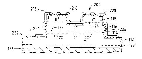
Referring now to Figure 9, there is shown a further embodiment of the
invention in the form of a bipolar transistor indicated generally by
300. The transistor 300 is of generally disc-shaped construction, and
is illustrated in section through a dismeter and through the disc
symmetry axis indicated by chain lines 302. It has as n' emitter 304, a
p' base 306 and an n' collector 308. An excluding contact 310 of
annular shape is connected to the base 306, the contact incorporating a
lower layer 312 and a p' upper layer 314. The transistor 300 has
electrical bias electrodes 316, 318 and 320 for the emitter 304, base
306 and collector 308 respectively.
The transistor 300 is formed of InSb and Ino.9Alo.lSb with dopant
species and concentrations as previously described; i.e. regions 304.
306. 308. 312 and 314 have compositions like to those of regions 118.
116. 118 (once more). 114 and 112 respectively in the heterostructure
100 of Figure 6.
The operation of the transistor 300 is as follows. Bias voltages are
applied to the electrodes 316, 318 and 320 to achieve transistor
operation with base current drawn through the base electrode 318.
Minority carriers are extracted from the base 306 by the n'p' interfaces
WO 92/12540 PCT/GB91/02270
f : r.
:W ly - '.
v L' J~
19
between the emitter 316 and base 306 and collector 308 and base 306,
which are extracting contacts. These carriers cannot be replenished
from the p'g' excuding contact formed by layers 312 and 314. The
minority carrier concentration therefore falls in the base 306, and with
it that of majority carriers from charge neutrality considerations.
This reduces the base conductivity. Conduction through the base 306
between the emitter 304 and collector 308 is therefore a function of the
base bias current in addition to the bias voltages on the emitter/base
and base/collector junctions. This makes it possible to achieve
relatively high dynamic range in the ratio of collector currents between
transistor "ON" and "OFF" states. The transistor 300 is therefore
suitable for digital switching applications.
Unlike the MISFET 200, it is important that carrier extraction and
exclusion take place over substantially all of the base 306 in order to
achieve good transistor performance. this is because a non-extracted
region extending between emitter and collector acts as a short circuit.
Referring now also to Figure 10, a further bipolar transistor embodiment
of the invention is shown and is indicated generally by 400. It is
similar to the transistor 300, and like features are like referenced
with a prefix 400 substituted for 300. The following description will
be directed to aspects of difference. As compared to the transistor
300, the transistor 400 has an additional annular base contact assembly
indicated by suffix "a" to its elements; these elements are an
excluding contact 410a, its lower and upper layers 412a and 414a, and a
base bias terminal 418a.
The additional base contact 410e is an A.C, signal input, and is
interposed between a D.C. bias current base contact 410 and an emitter
404. ifie transisrnr 4n0 _s D.C, bred as described for the previous
embodiment 300 using bias electrodes 416. 418 and 420. An A.C. signal
is then applied to the signal base electrode 418a, and this signal
produces modulation of the transistor current with consequent
amplification. The transistor 400 has the advantage that electrical
noise associated with the comparatively large base bias current does not
WO 92/12540 PCT/GB91/02270
~~H~w'~~!1~ f~ ._,
F 'J :J .:.. , '(J
appear on the much smaller A.C. input signal. This embodiment is
therefore appropriate for small signal analogue amplification.