Note : Les descriptions sont présentées dans la langue officielle dans laquelle elles ont été soumises.
2 0 ~ 9 PATENT
3791
TIME DELAY CONTROL FOR SERIAL DIGITAL VIDEO INTERFACE
AUDIO RECEIVER BUFFER
BACKGROUNl~ OF THE INVENTION
FIELI) OF THE INVENTION
S The present invention generally relates to digital audio information
processing, and particularly, to serial digital video interface audio sample
processing, and more particularly, to improvement of an audio channel first-
in first-out (FIFO) memory buffer enhancing audio signal quality and
maintaining synchronization with video ir~ormation.
DESCRIPTION OFTHE RELATED ART
A digital audio or video recording is no more than a series of numbers,
and hence can be copied through an indefinite number of generations without
degradation. This implies that the life of a recording can be truly indefinite,
because even if the medium begins to decay physically the sample values can
be copied to a new medium with no loss of information. For the highest-
quality post-production work, digital interconnection between such items as
. switchers, recorders and effects machines is highly desirable to avoid the
. degradation due to repeated conversion and filtering stages.
- Digitized audio and video information, although sampled at different
rates, can be multiplexed to provide cabling savings. A distinct advantage of
such multiplexed transmission is where numerous pieces of video/audio
equipment need to be interconnected in various ways for different purposes
- such as in a professional studio enviornment, a matrix distribution unit is
~, more easily realized than that of having separate video and audio
25 connections. A number of standards has been or is being developed to
establish guidelines for serial digital video interface in between studio
. ~ equipment which accomodates the video and audio information multiplex for
data transmission, such standards are the lnternational Radio Consultative
Committee (CCIR) Recommendations 656&601-2, and the proposed Society of
30 Motion Picture and Television Engineers (SMPTE) Standard 125M. In general,
in transmitting digital video images with a 27 MHz transrnission frequency, a
line of video information is separated from another by a horizontal sync
interval which provides a sufficient amount of time allowing the electron
, .
.,
. . -1 -
.,
':
~.
- ~ ~
209'36~9 PATENT
3791
beam steering mechanism to adjust from the end of one raster line to the
beginning of the next raster line. Ancillary information such as digitized
audio samples each having binary values and a specified word length may be
multiplexed into these sync intervals. Therefore, audio information
associated with a video frame image may be embeded between lines of that
video frame.
Despite the ease of transmission routing in between pieces of
equipment, i.e., carr,ving video and audio information on one cable instead of
two, however, within each equipment the combined video and audio signal
often requires demultiplexing in order to meet separate processing demands.
Since the audio information inserted into the sync intervals is typically
digitized at a sampling frequency different from 27 MHz (the transmission
frequency), for instance at 48 KHz, a FIFO memory buffer acting as an audio
data receiver is usually necessary to receive the extracted audio data at the
transmission frequency, 27 MHz, and to output audio data at the original
sampling frequency, namely, 48 KHz, ensuring synchronization with its
respective video data thereby.
Typically, there is a fixed number of audio samples per video frame,
for instance, in accordance to the aforementioned standards, there are 8008
audio samples for every 5 video frames in a 525 line/59.94 Hz system. In this
case, the number of audio samples in the FIFO buffer is maintained at a
particular value for every 5 video fields, meaning that each audio sample
stays in the FIFO buffer for approximately the same amount of time. If any
additional time delay or time advance relative to the video information is
int~oduced at the audio FI~O memory buffer stage, video and audio
information would be out of sync. There are various reasons for such an
additional delay or advance, one of which is that the FIFO memory buffer
output frequency drifts against its input frequency, for example, processing
images made by equipment not having the video and audio frequencies phase
locked. Another of which is the extenslve signal switching activities. Because
the total number of audio samples of any one video field may not be exactly
the same as its immediate successor field, switching activities such as
generating image composites from various sources may cause a gradual
increase or decrease of audio samples in the FIFO buffer. If uncorrected when
recorded and subsequently played back, lip sync occurs in that the audio
sound track would not follow its respective video images. The current
professional studio practice is to cause non-phase-locked digiti~ed
-2-
.
~ ~,
2~99~9 PATENT
3791
video/audio material to first undergo digital to analog conversion and then
analog to digital conversion at phase-locked rates to ensure relative frequency
stability. The practice is costly, and time consuming. The above described
practice has a further disadvantage in that it does not address the timing ill
effects created by the extensive signal switching activities.
As a result, unpleasant audible 'clicks' and 'pops' are generated when
the amount of data to be buffered exceeds the FIFO buffer size causing data to
be skipped or when the amount of data in the buffer is exhausted by output
causing data to be repeated. A single data skip or repeat is barely audible in
the high frequency spectrum and it is considered to be acceptable by the
current industry standard; but, more than one skip or repeat in series is
unpleasant to the ears. FIFO buffer overflow and underflow do not occur
under normal operations; however, the frequency drift and the extensive
signal switching may cause data skips and data repeats. CulTently, an
apparatus and method to prevent multiple audio data skips and repeats
occurring in series are not available for serial digital video interface.
The recent increase of video/audio switching and editing activities
such as digital special effects, in professional studios has underscored the
need for a low cost, improved performance, and ease of use apparatus and
method addressing the video and audio synchronization timing effects
brought on by a FIFO audio receiver buffer while complying with the SMPTE
Standard. The present invention satisfies this need by maintaining the FIFO
audio buffer at nominal fullness and delay by re-centering the buffer data size
as its fullness gets out of an arbitrarily specified range.
~ .
. 25 SUMMARY OF THE INVENTION
The present invention provides an improved FIFO memory buffer and
method for receiving a signal containing data samples and outpufflng these
samples at an output frequency while maintaining the amount of ~ne each
data element spends in the buffer before being read out. The apparatus and
30 method of the invention eliminate the lip sync problem and the audible
clicks' and 'pops' in playback by maintaining the FI~O buffer fullness within
a specified range.
A FIFO memory circuit receives data at an input write-data rate filling
up the memory storage cells therein. An output read-data signal clocks the
35 data out of the memory storage cells. The FIFO's fullness determined by the
-3-
, ~ .
. ~
. , . , : .. ~ :,
: .
2~99~89 PAIENT
3791
difference between its respective read (output) and wnte (input) address
pointers, in response to a Buffer Centering signal, is checked against a
variably and dynamically selected data s'7e range, a range that is smaller than
the FIFO buffer capacity. This specified range of data storage translates into a5 range of tolerable time delays for each buffered data element between FIFO
data write and data read. If at Buffer Centering time, the FIFO buffer fullness
is below the range's lower threshold or the lower time delay threshold, then
the FIFO's read address pointer is held so that the immediately preceding
read out data element is read out again, but only once. This provides more
lû time for the input write-data signal to accumulate more data elements into the
FIFO pushing the buffer fullness towards the center of the specified range. If
on the other hand, the FIFO buffer fullness is over the range's upper limit or
the upper time delay threshold, then the FIFO's write address pointer is held
so that the immediately preceding written in data element is written over, but
15 only once. This provides more time for the output read-data signal to reduce
the buffer fullness towards the center of the specified range.
An alternative embodiment of the present invention eliminates the
foregoing time delay problems associated with the magnetic audio
recording/playback channel. To ensure video and audio synchronization in
20 magnetic recording and subsequent playback, a FIFO buffer receives di~itized
audio samples in burst. at an input rate and output these samples at a
different, usually lower rate. A data element time delay inside the buffer
which is too long or too short will create lip sync, audio output mistracking
the video images. An overflow or underflow of the buffer with more than
25 one data element will cause the audible 'Cliclcc.' and 'pops'. The incorporaffon
of the present invention into such an audio channel by keeping the buffer
stored data size within a range will eliminate the lip sync and the audible
'clicks' and'pops'.
The above advantages of the present invention will become apparent
30 to those skilled in the art after having read the following detailed description
as accompanied by the figures of the drawing.
BRIEF DESCRIPTION OF THE DRAWINGS
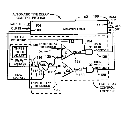
FIGURE 1 is a functional logic diagram of an embodiment in
accordance to the present invention.
.
-
~,
.
2 ~ 9 ~ PATENT
3791
FIGURE 2 is a functional block diagram of magnetic recording channel
incorporating an automatic time delay control buffer in accordance to the
present invention.
FIGURE 3 is a simplified diagram depicting a multiplexed signal
5 waveform timing relationship between video and audio information in
accordance with the proposed SMPTE Standard 125M.
DETAILED DESCRIPTION OF THE PREFERRED EMBODIMENTS
It is noted that corresponding circuit elements in all the drawing
Figures are designated by corresponding reference characters to facilitate
1 0 comparison.
Referring now to the drawings, and more particularly, to FIG. 1, there
is shown a functional logic diagram of an embodiment of the automatic time
delay control FIFO generally designated 100. This FIFO 100 includes a
memory logic 102 and a time delay control logic 105 (shown in broken lines).
The FIFO memory logic 102 functions are well known in the art and
therefore, for purposes of clarity, the inner details are not shown. It serves as
a data storage buffer which allows incoming data DATA IN to be written into
data-storage locations at a write-data rate CLK IN over a path 104. The
outgoing data DATA OUT is read out of the data-storage locations at a read-
20 data rate CLK OUT over a path 106. Therefore, data reading and writing are
controlled by separate clock signals CLK IN and CLK OUT over paths 108
and 110 respectively. The FIFO memory logic 102 is arranged so that the
incoming data DATA IN which is first written into the storage device is read
first out of the storage, hence, the name FIFO. FIFO memories are often
25 provided as semiconductor integrated-circuit devices or as a part of an
Application-Specific IC (ASIC). ln the }~IFO memory logic 102, a read-
address pointer READ ADDRESS keeps track of the address of the first-
written information and a write-address pointer WRITE ADDRESS keeps
track of the next available memory location. A data element, either in serial
30 or parallel form having a length of a fixed number of binary bits, goes directly
into a memory cell from data input terminal of the FIFO located at the
memory logic 102 end of the path 104. The data element from the memory
cell goes directly to the output terminal, located at the memory logic 102 end
of the path 106, of the FlFO memory without being serially transferred from
35 storage cell to storage cell. Reading and writing of data are controlled by
. ; . .:
. .
: :
209~6~9 PATENT
3791
separate clock signals CLK rN and CLK OUT over paths 108 and 110
respectively.
The time delay control logic 105 includes a signal summation logic
SUM, a pair of comparator logics C1 and C2, a threshold adjust logic 140, and
5 a pair of address hold logics G1 and G2. The write-address pointer WRITE
ADDRESS and the read-address pointer READ ADDRESS from the memory
logic 102 are applied to the input terminals of the signal summation logic
SUM. Signal WRlTE ADDRESS goes into SUM via its non-inverting terminal
(+) over a path 116. Signal READ ADDRESS goes into SUM via its inverting
10 terminal (-) over a path 118. The resulting buffer fullness signal BF is applied
to input terminal Q1 of the comparator logic C1 and input terminal P2 of the
comparator logic C2 via paths 120 and 122 respectively. An arbitrarily set
delay range is delimited by signals LOWER DELAY THRESHOLD which
feeds into P1 terminal of the comparator logic C1 over path 124 and UPPER
15 DELAY THRESHOLD which feeds into Q2 terminal of the comparator logic
C2 over path 126. Both of these thresholds are set and adjusted by the
threshold adjust logic 140. The output of C1, P1>Q1, is 'true' only if the buffer
fullness signal BF is smaller in value than that of the LOWER DELAY
THRESHOLD. On the other hand, the output of C2, P2~Q2, is 'true' only if
20 the buffer fullness signal BF is larger in value than that of the UPPER DELAYTHRESHOLD. The address hold logic G1 receives the signal P1>Q1 into one
of its input terminals over path 128 and G2 receives the signal P2>Q2 into an
input terminal over path 130. A delay control signal BUFFER CENTERING is
applied to the other input terminals of G1 and G2 over paths 132, and 134.
25 The address hold logic Gl will output a HOLD READ ADDRESS ir~truction
to the memory logic 102 over a path 136 when signals BUFFER CENTERlNG
and P1>Q1 are both 'true'. Analogously, the address hold logic G2 will issue
a HOLD WRlTE ADDRESS instruction to the memory logic 102 over a path
138 when signals BUFFERING CENTERING and P2~Q2 are both 'true'.
Operationally, data elements with a speciflc word length are
asynchronously clocked into the automatic time delay control FIFO 100 by
CLK IN. Typically, these data elements are clocked out by CLK OUT in the
order in which they were received. Each data element spends a certain
amount of time in the FIFO 100 waiting to be read out. This delay period will
be longer when the FIFO memory is on the average nearly full than when the
FIFO memory is typically close to empty. The time delay control logic 105
assesses the buffer fullness as reflected by the signal BF whenever the control
.
,.
.
... ..
,, ~; , " ' . ' '
. , , . , ~ . . ~ .
~ .
2~)99~89
PATENT
3791
logic 105 is enabled by the signal BUFFER CENTERING, an appropriate clock
frequency signal which may be varied by hardware or software system
components. The buffer fullness signal BF is compared against a designated
'fullness' range (or in other words, a designated 'time delay' range). If the
5 buffer fullness signal BF indicates a level that is out of the range established
by LOWER DELAY THRESHOLD and UPPER DELAY THRESHOLD, then
automatic buffer size centering actions will occur to pull the buffer fullness
towards the middle of the specified delay range. If the fullness is over the
UPPER DEEAY THRESHOLD, a HOLD WRITE ADDRESS instruction is
10 issued holding the WRITE ADDRESS for one write cycle so to cause a data
element to be skipped allowing the buffer size to fall within the specified
range; if the fullness is below the LOWER DELAY THRESHOLD, a HOLD
READ ADDRESS instruction is issued holding the READ ADDRESS for one
read cycle so to cause a data element to be repeated allowing the buffer size to15 reach within the specified range. Implementations of the memory logic 102
and the time delay control logic 105 include but not limited to digital
integrated circuits, ASIC technology or a combination of hardware and
microcode instructions. An alternative embodiment of the present invention
would include the time delay control logic 105 as a part of the operation in a
20 programmable controller.
Referring now to FIGS. 2 and 3, there is provided another embodiment
in accordance with the present invention constituting a magnetic recording
channel generally designated 200. The magnetic recording channel 200
includes a signal extraction logic 210, a video channel logic 220, an audio
25 channel logic 230 which comprises an automatic time delay control first-in
first-out memory buffer (ATDC-FIFO) logic 100 and an audio processing logic
250, and a magnetic recording apparatus 260. The magnetic recording
channel 200 receives a multiplexed signal INPUT WAVEFORM containing
both the video and audio information and then separately records the video
30 and audio information onto a magnetic medium by the magnetic recording
apparatus 260 with an appropriate data format and timing synchronization.
INPUT WAVEFORM on path 212 conforms to the video and audio timing
relationship as it is crudely represented by signal 300 (See FIG. 3). Typically,in between every active video line, there is a horizontal sync time period, H-
35 SYNC. This H-SYNC is a time period where video information is not present,
allowing the electron beam steering mechanism to move from the end of one
raster line to the start of the next line. Industry usage, such as the proposed
3 9 l,~ ~j 8 ~ PATENT
3791
SMPTE Standard 125M describing a serial digital video interface, allows
ancillary infonnation such as digitized audio samples to be inserted into these
sync periods. INPUT WAVEFORM feeds into the signal exkaction logic 210
over a path 212, the output of which, VIDEO and AUDIO signals, feed into a
video channel 220 over path 222 and an audio channel 230 over path 232,
respectively. AUDIO data is first applied So ATDC FIFO 100 over path 232,
and subsequently encoded in audio processing logic 250 via path 242 to a
designated data format such as that in accordance with the Audio
Engineering Society (AES3-1985, ANSI S4.40-1985) before being recorded by
the magnetic recording apparatus 260 via path 252. AUDIO is represented by
signal 310 wherein the square wave pulses each contains a number of
digitized audio samples which each having a fixed number of binary data
bits. VIDEO, the audio sample-striped INPUT WAVEFORM, is processed in
the video channel 220 and recorded onto the magnetic medium by the
magnetic recording apparatus 260 via path 262.
For a typical FIFO capacity, for examples,16 or 64 words, each word or
each data element having a fixed number of binary data bits, a range of
tolerable mean input-output delay can be arbitrarily set and sought to be
maintained to avoid lip sync problerns when audio sound mistracks the video
20 images. Furthermore, having such a range eliminates the unpleasant 'clicks'
and 'pops' when more than one data element is repeated or skipped in series
because it enables data skip or data repeat to occur only one at a time.
Operationally, in accordance to the proposed SMPI E Standard 125M,
for a given amo nt of video, there will always be a certain number (+/-1) of
25 audio samples. An audio sample can have up to several words and each
word may contain a fixed number of data bits. These samples are placed in
the horizontal ancillary data region, H-SYNC, of INPUT WAVEFORM. This
multiplexed format applies to both component and composite technology.
Regardless, in the magnetic recording channel 200, VIDEO and AUDIO are
30 processed separately and therefore synchronization of the two is critical
because a slight time delay difference will cause either lip sync or an audible
'click' or 'pop'. ATDC-FIFO 100, detailedly described above as in FIG. 1, is
designed to output audio samples with a certain amount of time delay~ In
other words, over a field or frame, one would expect a nominal number of
35 audio samples. However, if the switching activities or the relative frequencydrift is allowed to persist, then the buffer could overflow or underflow
. . .
,~
. .~ .. .
;.
2 ~3 g ~ PATENT
3791
causing a time delay unaccountable in the video channel 220 and therefore
producing aforementioned problems.
If a signal at a reasonable rate, such as frame or field rate, is used to
check how full the receiving memory buffer is, or in other words, how much
5 delay audio samples incur in the receiving memory buffer, then a decision
can be made whether too many or too few audio samples are in a fixed
number of video frames. A sample may be skipped or repeated to keep the
audio delay within a certain range and lceeps the buffer from overfowing or
underflowing. If the buffer is too full (or data delay is too long) when
10 BUFFER CENTERING is 'true', one sample can be skipped by not allowing
the buffer WRlTE ADDRESS to increment for one write cycle. If the buffer is
too empty (or data delay is too short) when BUFFER CENTERING goes high,
one audio sample can be repeated by not allowing the read address to
increment for one read cycle. Ultimately, signals coming out of the video
channel 220 and the audio channel 230 will reach the magnetic recording
apparatus 260 in appropriate synchronization.
The present invention and its various embodiments may be
implemented in various types of digital logic families or technology. ~ogic
reduction and transformation techniques may be employed to utilize other
20 arrangements of gates or logic elements which are functionally equivalent to
the one descnbed here.
:.
!
.
.. , ~ ,
.