Note : Les descriptions sont présentées dans la langue officielle dans laquelle elles ont été soumises.
EN9-92-108 21~023~
SWITCH-BASED MICROCHANNEL PLANAR APPARATUS
FIELD OF THE INVENTION
The present invention relates to digital computer systems
comprised of several or many computing and/or input/output
elements, and the ability of the said individual elements to
perform high speed, low-latency c~ Inications with each
other in a parallel fashion over switching networks.
GLOSSARY OF TERMS
Card slots
Receptacle connector3 mounted on a planar for the
purpose of receiving processor or expansion cards.
Expansion Card
A board of components that function together as a
co-processing or I/O element. The card board has
multiple wiring planes used to interconnect all
components mounted on the board. The card board has a
connector element used to connect the card to the
planar (usually the card connector is inserted into the
planar connector receptacle). The active components on
the card usually include a co-processing and/or I/O
element, remote memory, and an I/O interface in the
form of a multi-drop bus that connects to the planar
through the card connector for co ~nication to other
processor or I/O cards.
.
Functional Elements
Any processor or I/O device connected in the form of a
processor card or expansion card to the multi-stage
network incorporated on the disclosed planar.
I/O Card
Another term for expansion card.
MC Converter
EN9-92-108 210 ~ ~ 3 ~
A functional converter that converts the standard
MicroChannel bus protocol to the switching network
protocol. MicroChannel is a trademark of IBM for the
I/0, Multi-drop bus used in most IBM Per~onal Computers
and other machines. The description uses MicroChannel
to refer to a multi-drop bus.
MCC
Abbreviation for MC Converter.
Node
A functional element of the system comprised of one or
more processor and/or expansion cards interconnected by
a standard bus, which in turn connects to to the
switching network as a single port of the network.
Nodal element
Another term for node, which has the same meaning.
Planar
A interconnection board or motherboard having multiple
wiring planes. The planar contains active components,
such as a multi-stage switching network, and inactive
components, such as connector slots capable of
receiving processor or expansion cards. The planar
provides the interconnection wiring amongst the said
;~ cards.
Port
~ A single bi-directional entry and exit point to a
~~ switching network.
:
~ Processor Card
; A board of components that function together as a
processing element. The card board has multiple wiring
planes used to interconnect all components mounted on
the board. The card board has a connector element used
to connect the card to the planar (usually the card
connector i~ inserted into the planar connector
receptacle). The active components on the card usually
include a computing element, memory (local and cache),
:.-
EN9-92-108 2 ~ O ~ ~ 3 ~
and an I/O interface in the form of a multi-drop bus
that connects to the planar through the card connector
for communication to other processor or I/O cards.
Receiving Node
A functional element of the system comprised of one or
more processor and/or expansion cards interconnected by
a standard bus to a switching network, which is
receiving data transmitted over the switching network.
Sending Node
A functional element of the system comprised of one or
more processor and/or expansion cards interconnected by
a standard bus to a switching network, which is
transmitting data over the switching network.
BACKGROUND OF THE INVENTION
Multi-stage switching networks are gaining acceptance as a
means for inter-connecting multiple devices within modern
digital computing systems. In particular, in parallel
systems it is common to use a multi-staged switching network
to interconnect N system elements, where N can be several or
thousands of processors or combinations of processors and
other system elements.
The state-of-the-art interconnection approaches have
centered around multi-drop busses, which have many short
comings, the primary of which is limited performance and
expansion. The problem exists in bus-based processors that
there is an ever increasing need for better I/O bus
performance and the attachment of more I/O options. This is
in direct conflict with the nature of a multi-drop bus
technology, which loses performance as more and I/O options
are added as taps to the bus. In general, standard bus
architectures such as the MicroChannel (IBM Trademark) have
selected a performance goal and thus limited the number of
I/O taps permissible at that performance level. In the case
of the MicroChannel the result is that 8 taps (or expansion
cards) is the maximum number of allowable bus taps to permit
bus operations to occur at 200ns cycle times. As a result,
EN9-92-108 4 210 ~ ~ 3 ~
based-based system user~ are beginning to find that the I/O
capability is not sufficient to meet their needs. For years
people having been looking for means of increa~ing the I/O
capability of bus-based systems.
Bus-based system performance is limited because only one
user can have access to the bus at any given time. The
expandability is limited because of the electrical
characteristics of the multi-drop bus including drive
capability, noise and reflections.
On the other hand, MicroChannel and bus-based machines are
relatively inexpensive and constantly increasing in
processor performance capabilities. These machines and their
expansion cards represent investment dollars, and owners
wish to use and build on this investment for many years.
The present invention provides a means of using bus-based
processor cards and bus-based expansion cards at improved
performance and expandability levels by disclosing a new
planar interconnection means.
The present invention interconnects multiple bus-based cards
by adapting the existing bus interface to allow each card or
sets of multiple cards to be interconnected via a high speed
switching network. This enables the individual bus-based
cards to CG lnicate with low-latency messages and to
interact as a parallel ~ystem. Now many communications can
take place simultaneously in parallel and expansion can be
virtually unlimited. This allows for use of investment, yet
it overcomes all the limitations placed upon a single
bus-based architecture.
i
Many state-of-the-art switch solutions do not provide the
switching network characteristics and low-latency concepts
required for modern interconnect systems. The
characteristics that are required include the ability to
dynamically and quickly establish and break element
interconnections, to do it cheaply and easily in one chip,
to have expandability to many thousands of elements, to
permit any length, non-calibrated interconnection wire
lengths, to solve the distributed clocking problems and
EN9-92-108 5 210~23~
allow future frequency increases, and to permit parallel
establishment and data transmittal over N switching path~
simultaneously.
The distributed and fully parallel switch utilized herein to
provide the required interconnect properties is an
asynchronous, low latency, inter-node switch adapted in the
present invention to perform the switching of converted bus
interfaces at low latencies and high bandwidths. The switch
provides a circuit switching capability at high bandwidths,
and includes distributed switch path connection set-up and
tear-down controls individually within each switch - thus
providing parallel set-up, low latency, and elimination of
central point failures. We will further describe in the
detailed description a way whereby the above switch and the
present invention can be used to solve the bus-based
processor interconnection problem effectively.
Often systems require multiple paths through multi-stage
switching networks to improve performance, provide fault
tolerance, and prevent blocking. The above mentioned switch
i8 adapted by the present invention to provide multiple
paths. An earlier work at IBM by Peter Franaszek, as
described in his work entitled "Multipath Hierarchies in
Interconnection Networks" described two hierarchical paths
for a network, one providing low-latency message transfer
and the other providing guaranteed-delivery of a message
transfer and the other providing guaranteed-delivery of a
message at a longer latency. A message is attempted over
the low-latency path first. If the transmission fails due
to blocking or contention, it is retransmitted over the
guaranteed-delivery path. This allows usually about 90% of
the messages to be sent successfully over the low-latency
path, and guarantees the delivery of a message that gets
blocked on the low-latency path due to retransmissions.
.
- U.S. Patent 4,952,930 to P. A. Franaszek et al. issued Aug.
28, 1990 described the approach which used a second buffered
path, which i~ in some ways similar to the current approach.
However, it suffered by its requirements of a plurality of
switches to implement it. While there would be no impediment
EN9-92-108 6 21~
to our adopting the teachings of this patent there remained
a need for a simpler and yet more flexible approach to
create a multi-stage network.
Multi-stage networks have become an accepted means for
interconnecting multiple devices within a computer ~ystem.
They are a replacement for the traditional crossbar
interconnection. The crossbar is still a most efficient
method of network interconnection, but it tends to be
impractical for large systems. An NxM crossbar permits
total simultaneous interconnection, where all the N devices
can be communicating simultaneously with different members
of the set of M devices. The crossbar is "non-blocking"
because their is nothing internal to the crossbar which
prevents any given N device from connecting to an M device
which is IDLE (is not connected to some other N device). If
an N device desires to connect to an M device which is BUSY
(previou~ly connected to some other N device), no connection
can be made until the previous connection is broken --
however, this is referred to as "contention" and is not
called "blocking".
When N and M become large (usually greater than 32 or 64) it
becomes very unwieldy to build crossbars since there
complexity increases at an NxM rate and their pin count
increa~es at an (NxM)xW rate, where W= the number of pins
per port. Thus large networks are usually built from
multi-stage networks constructed by cascading several stages
of smaller crossbars together to provide an expanded
network. The disadvantage of multi-stage networks is that
they are "blocking", i.e., a connection might not be able to
be made to an IDLE M device because there is no path
available in the network to provide the necessary connection
to the IDLE device.
Among other patents which might be reviewed are: U.S.
Patent 4,914,571 to A. E. Baratz et al. issued Apr. 3,
1990 which describe~ a method of addressing and thus how to
find re~ource~ attached to a network, but does not deal with
the hardware for the actual network itself.
:
-
EN9-92-108 7
2la~.~3~
U.S. Patent 4,455,605 to R. L. Cormier et al. issued
June 19, 1984 which is for a bus oriented system, it is not
a multi-stage network. Similarly, U.S. Patent 4,396,984 to
E. R. Videki, II issued Aug. 2, 1983 is for an I/O bus
channel, not a multi-stage network. U.S. Patent 4,570,261
to J. W. Maher issued Feb. 11, 1986 is for fault recovery
over a bus oriented ~ystem, not a multi-stage network.
U.S. Patent 4,207,609 to F. A. Lui~ et al. issued June
10, 1980 illustrates an I/O bus channel so that those in the
art will understand the differences between the subject
matter. It is not a multi-stage network.
U.S. Patent 4,873,517 to A. E. Baratz et al. issued Oct.
10, 1989 is for a totally different type of network, not an
equi-distant multi-stage network like that which we will
describe, and also, U.S. Patent 4,932,021 to T. S. Moody
i~ued June 5, 1990 for bus wiring paths inside a computer
box, it is not a multi-stage network. U.S. Patent
4,733,391 to R. J. Godbold et al. issued Mar. 22, 1988
illustrates a ring interconnection network, which is unlike
a multi-stage network. U.S. Patent 4,811,201 to B. R.
Rau et al. issued Mar. 7, 1989 are not applicable to a
multi-stage network. U.S. Patent 4,754,395 to B. P
Weisshaar et al. issued June 28, 1988 is for a ring
interconnection network.
SUMMARY OF THE INVENTION
'
The invention is a modularly expandable switch-based planar
apparatus for inserting multiple bus-based processor cards
and/or expansion cards and interconnecting the said cards
via a multi-stage switch network which resides on the
invention planar. The multi-stage network is used to
interconnect bus-based cards (cards that provide bus
interfaces - like MicroChannel cards providing the standard
MicroChannel bus and connectors). The switching network is
built into the planar.
The card~ themselves require no modification or change of
any kind, the connection to the planar is made as if the
EN9-92-108 8 21~ ~ f~ ~ ~
planar contained the standard multi-drop bus
interconnection. However, the disclo~ed planar is a new
concept that contains only the point-to-point wiring for
interconnecting multiple switch stages, rather than
supporting the standard multi-drop bus connections. All
processors and expansion cards are still fully
interconnected and capable of sending communications or
messages between any two elements. The communication media
is switch-based and is fully parallel, supporting n
transmissions simultaneously, where n is the number of
functional elements interconnected by the switching network.
The preferred switching means i8 a basic digital
asynchronous and unbuffered switching concept. Such
apparatus provides a switching network communication
structure that has the characteristic of simplicity of
implementation, and does not require data buffering or data
conversion of any kind. It establishes or breaks
connections instantaneously and is, therefore, dynamically
changeable with a very quick response time. It has the
capability of resolving requests to establish connections in
a parallel manner, where n connections can be established or
broken at the same time (where n = the number of elements of
the system which are communicating via the switching
network). Thus, the number of connections that can be made
or broken simultaneously scales directly with the size of
the system. This capability enables the invention apparatus
to handle multiple short messages very efficiently. In
addition, the new apparatus is devoid of synchronization
requirements or wire length restrictions. It also has the
ability to track the speed improvements of new technologies
and to increase performance as the technology used to
implement the invention apparatus improves. In addition,
the switching apparatus can be cascaded with other identical
apparatus devices to form interconnection networks among any
number of system elements or nodes. Said network would have
the characteristics for full parallel interconnection.
BRIEF DESCRIPTION OF THE DRAWINGS
EN9-92-108 9 2 1a ~3 ~
FIGURE 1 illustrates generally our preferred embodiment of
the present invention of the Switch-based MicroChannel
Planar apparatus, which has the capability of
interconnecting multiple bus-based processor and/or
expansion cards.
FIGURE 2 illustrates a four input and four output (4 X 4)
crossbar switching apparatus, which has the capability of
providing the disclosed fully parallel switching means for
interconnecting up to four nodes.
FIGURE 3 illustrates the interconnections required to a four
input and four output (4 X 4) crossbar switching apparatus
to provide full interconnection amongst four nodes.
FIGURE 4 shows a typical method for cascading the 4x4
disclosed embodiment of the invention switching apparatus to
accommodate systems having more than 4 nodes.
FIGURE 5 shows a schematic block diagram of the simple
digital data flow and control path implementations of the
4x4 cro~sbar switching apparatus, which has the capability
of being used with the present invention to provide fully
parallel switching means for interconnecting up to four
system nodes for the purpose of transferring digital data.
FIGURE 6 illustrates a typical method for generating
parallel control and and multiple line serial digital data
information to be sent to the 4x4 prior parent embodiment of
the invention switching apparatus over four synchronous data
lines.
.
FIGURE 7 shows a typical timing diagram for routing the
digital interface signals arriving at one input port of the
4x4 prior parent embodiment of the invention switching
apparatus to one output port.
FIGURE 8 illustrates the typical method of selecting and
establishing a transmission path through a network comprised
of the invention switching apparatus for the purpose of
sending digital data from one node to another.
.
EN9-92-10~ 2~0Q~S
FIGURE 9 illustrates a typical physical embodiment of the
Switch-based MicroChannel Planar apparatus showing how the
switching network is incorporated into the said planar.
FIGURE lO illustrates the planar interconnections required
to interconnect 8 nodes on the Switch-based MicroChannel
Planar apparatus as a stand-alone system.
EIGURE 11 illustrates how the number of nodes in the system
can be expanded above 8 nodes by interconnecting multiple
Switch-based MicroChannel Planars, each incorporating a
portion of a distributed multi-stage network capable of
interconnecting larger number of nodes.
FIGURE 12 illustrates how the number of nodes in the system
can be expanded above 64 nodes by interconnecting multiple
Switch-based MicroChannel Planars to a supplemental switch
network, where the entire switch network is distributed
across multiple Switch-based MicroChannel Planars and the
supplemental switch network.
!
DETAILED DESCRIPTION OF THE PREFERRED EMBODIMENTS
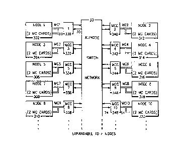
Turning now to the drawings in greater detail, FIGURE 1,
shows the preferred method of interconnecting n nodes via
the Switch-based MicroChannel Planar. The entire system is
composed of individual nodes (302,304,306,308,310,312,
314,316,318,320,etc.) connected to individual MicroChannel
Converter units (MCC's 330,332,334,336,338,340,342,344,
346,348,etc.), which in turn connect to the switch network
30. A typical node is shown by block 2 as being comprised
of 2 MicroChannel Cards (MC CARDS); these cards can be
either processor cards or expansion cards in any
combination. The number of MicroChannel Cards per node can
vary with each individual node and can be composed of from 1
to 8 cards; however, the preferred embodiment shown in
Figure 1 assigns 2 MC CARDS to each node. These MC nodes
can either connect as a direct point-to-point wired
MicroChannel bus to the assoclated MCC 330 unit in the case
where a node is comprised of only one MC card, or these MC
CARDS can connect as a multi-drop MlcroChannel bus to the
EN9-92-108 21 ~ ~ 2 3 ~
MCC 330 to give the node an increased card count and
increased nodal flexibility. The MicroChannel bus
connection of 2 cards per node to a single MCC 330 function
is denoted in Figure 1 as a unique MicroChannel bus labelled
MCl to indicate that it is an entirely different and
isolated MicroChannel bus from the other similar MC busses,
such as MC2, MC3, etc. In turn, each MCC functional block
connects by point-to-point wiring only to switch network 30.
Switch network 30 can be any type of multi-stage, torus, or
hypercube network that permits either small or massive
expansion by permitting several or massive number of nodes
to interconnect. However, the preferred embodiment of the
switching means as noted above is a basic digital
asynchronous and unbuffered switching concept which is a
unidirectional switch implementation. The preferred
embodiment uses only unidirectional interfaces, and
therefore Figure 1 shows the switch interface 70 to be
comprised of two unidirectional sets of lines, one carrying
data from node lA, and one carrying data to MCCl from the
switch network, and one carrying data to the switch network
from MCCl.
Figures 2 to 8 refer to a 4X4 crossbar implementation of the
previously mentioned switch to illustrate the principles and
speed of the switching concept.
Referring to Figure 2, the preferred embodiment is a 4x4
switching apparatus 12, where the function of the present
invention is to provide a means of connecting any of 4 sets
of digital, analog, or optical inputs on a mutually
exclusive basis to any one of the unused 4 output ports.
The 4x4 switching apparatus 12 can support up to 4
simultaneous connections at any given time. For instance,
Input 1 could be connected to Output 3, Input 2 to Output 4,
Input 3 to Output 2, and Input 4 to Output 1.
The invention switching apparatus 12 is unidirectional,
which means that data flows in only one direction across the
~aid switching apparatus 12, that being from input to
output. Switching apparatus 12 interfaces are defined in
EN9-92-108 12 21~ ~ ~J 3 ~
detail in Figure 2. The set of lines 31, 32, 33, and 34 at
each in-port to the switching apparatus 12 are identical in
number and function to the set of lines 41, 42, 43, and 44
at each out-port. The sets o~ inter~ace lines to each input
and output port contain seven unique ~ignals: 4 digital data
lines, and 3 digital control lines (VALID, REJECT, and
ACCEPT). The signals at each port are differentiated by a
prefix of INX- or OUTX- indicating the direction and number
of the port (X) that they are associated with. The four
digital data and one VALID lines have a ~ignal flow in the
direction going from input to output across switching
apparatus 12, while the digital REJECT and ACCEPT control
lines have a signal flow in the opposite direction.
Each unidirectional switch interface set requires only 7
signals, as shown in Figure 2, to transmit and control and
data through the network 30 -- the digital data and control
transfer width is l/2 byte (4 bits) at a time. The signals
required are:
DATA:
4 parallel signals used to command switch connections
and transmit digital data messages or digital control
headers.
VALID:
When active, indicates that a digital message, control
header, or analog waveform is in the process of being
transmitted. When inactive, indicates a RESET command
and causes all switches to reset to the IDLE state.
i
REJECT:
Signal flow is in the opposite direction from the DATA
and VALID signals. When active, it indicates that a
REJECT or error condition has been detected.
ACCEPT:
Signal flow is in the same direction as the REJECT
signal. When in the low state, it indicates that a
message is in the process of being received and checked
EN9-92-108 210~3~
for accuracy. When active, it indicates the message
has been received correctly.
As illustrated by FIGURE 3 the switching apparatus would be
provided for a node having a plurality of input and output
ports, and would comprise the connection control circuit for
each input port, and a multiplexer control circuit for each
output port for connecting any of I inputs to any of Z
outputs, where I and Z can assume any unique value greater
or equal to two.
Figure 3 shows a 4x4 cros~bar switching apparatus, where the
switching apparatus 10 is unidirectional, which means that
data flows in only one direction across the said switching
apparatus 10, that being from input to output. Although the
said switch apparatus 10 is unidirectional, it supports
bidirectional cc lnication amongst four nodes (20, 22, 24,
and 26) by connecting the 4x4 switching apparatus 10 as
shown in FIGURE 3. Each node 20, 22, 24, and 26 has two
sets of unidirectional interconnecting wires, one going to
the switch 10 and one coming from the switch 10. The dashed
lines internal to the switching apparatus 10 indicate that
the function of the said switching apparatus is to connect
an input port such as INPUT PORT 1 to one of four possible
output ports. The switching apparatus 10 providès exactly
the same function for each input port, allowing it to be
connected to any unused output port.
I
Referring to FIGURE 4, a method is illustrated for
increasing the number of nodes in a system by cascading
eight switching apparatus 10 blocks. The eight cascaded
switches are denoted as lOA through lOH to indicate that
they are identical copies of switching apparatus 10, varying
only in regards to the wiring of their input and output
ports. It can be noted that any of sixteen nodes can
cc icate to any other node over a connection that passes
through exactly two of the switching apparatus 10 blocks.
For instance, Node 5 can send messages to Node 15 by
traversing switch lOB and switch lOH. Slnce all connections
are made through two switching apparatus 10 blocks, the
network comprised of the eight switching apparatus 10 blocks
EN9-92-108 14 21~0~
i~ referred to as a two stage switching network. Other
multi-stage networks can be configured from ~witching
apparatus 10 blocks by using three stages, four stages, etc.
in a similar manner.
Referring to EIGURE 5, a functional diagram of the simple
data flow across switching apparatus 10 is illustrated. The
VALID and four data lines at each input port, inside the
switch, and at each output port are represented by a single
line in FIGURE 5 for simplicity. For instance, the VALID
and four data lines entering switch 10 at IN PORT 1 go to
five internal functional blocks of switching apparatus 10;
these are blocks 50A, 60A, 60B, 60C, and 60D. Block 50A
makes the decision as to which of the four possible output
ports are to be connected to input port 1. The VALID and
four data lines from each input port go to each output
multiplexer block (60A, 60B, 60C, and 60D); this makes it
possible to connect any input port to any output port. Each
of the foùr output multiplexer blocks (60A, 60B, 60C, and
60D) is uniquely commanded from each of the control blocks
(50A, 50B, 50C, and 50D) as to which of the four possible
sets of input port lines is to be gated through to each
output port. For instance, control block 50A can cc ~n~
multiplexer 60C to connect input port 1 to output port 3;
control block 50B can command multiplexer 60A to connect
input port 2 to output port 1; and control block 50C can
C~ ~n~ multiplexers 60B and 60D to connect input port 3 in
a multi-cast fashion to output port 2 and output port 4.
All three connections are capable of being established
- simultaneously or at different times. At the same time that
multiplexers 60A to 60D form connections to move the VALID
and data ~ignals across switch 10 with a unidirectional
signal flow from input port to output port, multiplexer 61D
and AND gate 63D form signal connections for the REJECT and
ACCEPT signals, respectively, with a signal flow in the
opposite direction of output port to input port (typical
implementations are shown by blocks 61D and 63D -- similar
blocks are associated with each input port). These REJECT
~ and ACCEPT signal~ provide a positive feedback indication to
switch 10 of actions taken either by subsequent switch 10
stages in a cascaded network or by the device receiving and
EN9-92-108 15
interpreting the VALID and four data signals. A control
header or digital message being transmitted through
switching apparatus 10 over the four data signals under
control of the VALID signal can be REJECTed by any network
stage if it is unable to establish the co An~ed connection
or by the receiving device if it is not capable of receiving
the me~sage at this time or if it detects an error in the
transmission. The receiving device also has the capability
of confirming the correct arrival of a command or message
(without errors being detected) by pulsing the ACCEPT
signal. Since the REJECT and ACCEPT signals go in the
opposite direction from the data flow, they provide a means
of reporting back a positive indication to the sender on
whether the attempted transmission was received correctly or
re;ected.
Referring to Figure 6, blocks 56, 52, and 54 illustrate a
typical method for generating multi-line (parallel)/serial
digital data in the form of a message which can be
transmitted to and across switching apparatus 14, which is a
partial drawing of the switching apparatus 12. Similar
parallel/serial data generation logic as provided by 56, 52,
and 54 can be used at each of the other input ports to
switching apparatus 12. Each set of input data lines
provides 4 serial data lines to a given input port which is
synchronized to the same clock by the four shift registers
51 which create the parallel/serial data by shifting four
synchronized lines of data 31 as controlled by the same
identical clocking signal (100 MHZ in Fig.6). However, the
four different input port sources (31, 32, 33, and 34) to
switching apparatus 14 can be asynchronous to each other,
being based on different, non-synchronized, 100 MHZ clocking
signals.
The process for sending parallel/serial messages through
switching apparatus 14 involves FIF0 56, which accumulates
data messages to be transmitted. The next entire message to
be transmltted is moved to buffer 52. The message stored in
buffer 52 is moved to ~hift registers 54 in preparation for
transmittal and the data is dispersed across the four shift
registers 54 by placing data bit 0 into the first bit of
EN9-92-108 16 21D~23~
shift register 1, data bit 1 into the fi~st bit of shift
register 2, data bit 2 into the first bit of shift register
3, data bit 3 into the first bit of shift register 4, data
bit 4 into the second bit of shift register 1, etc. Shift
registers 54 then begin to send serial data to switching
apparatus 14 over four synchronized data lines, in such a
manner that the parallel/serial data flows continuously
until the entire message has been transmitted. The switch
apparatus 14 uses the first eight bits transmitted (in the
first two clock cycles of serial data over interface 31 from
serial registers 54 to switching apparatus 14) to select and
establish a connection path through the switching apparatus
14. The example in Figure 6 illustrates via dashed lines,
the switching apparatus establishing a temporary connection
between input port 1 (31) and output port 2 (42), such that
each of the eight individual lines in interface 31 are
uniquely and directly connected to each of the corresponding
lines in interface 42.
Referring to Figure 7, typical serial waveforms are shown
for both input and output ports of the switching apparatus
14. The switch removes the first 8 bits of the serial
transmission as sent by shift registers 54 and uses them to
make and hold a connection, such as interface 31 to
interface 42. The remainder of the serial message in our
example is transferred directly from interface 31 to
interface 42, so that interface 42 sees that exact same
me~sage that interface 31 receives, minus the first 8 bits
and delayed by the circuit delays encountered by the serial
data as it traverses the switching apparatus 14. Switching
apparatus 14 does not buffer or re-clock the serial data
entering via interface 31 in any manner; it merely reflects
as quickly as possible the input waveforms it receives over
interface 31 to output interface 42 without changing them in
any way, except to strip off the first 8 bits.
The convention for indicating to a switch 14 input port over
an interface (such as 31) that there is no transfer in
progress, is to issue continuous IDLE commands, which are
denoted by the 4 data lines and the VALID control line being
held at logical O's. The detection of a logical 1 on any of
EN9-92-108 17
21Q~2~
the input lines will signify the departure from the IDLE
state and signify to the switch that a selection and
transfer i5 beginning. Likewise, the output lines from the
switch will be held in the IDLE state (at all O's), when
there is no active transfer in progress.
In general, all switches require a path selection method,
whereby they are commanded which connection (input port to
output port) to establish. For switching apparatus 10, the
path selection cc 9nd is transmitted to the switch over the
same interface that the data is transferred; i.e., the 4
data lines associated with each input port. Selection
information must be transferred prior to the data, so that
the cc. ~n~ed interconnections can be established and the
data can then flow to the c ~nded destination. The
selection information need NOT identify an input port number
(1 to 4), because it is arriving at the switch over a
specific input and the switch already knows what input
number it i8 receiving data on. Therefore, the selection
information need ONLY specify the number (l to 4) of which
one of the four output ports of switching apparatus 10 to
which to connect. The method of path selection recommended
here is one out of N encoding with a return to zero (called
a DEAD FIELD).
Referring to Figure 8, a typical example of the exact serial
bit patterns and control signal activation is shown for
sending control and digital data information to switching
apparatus 10. The example references the cascaded, two
stage switching network shown in Figure 4 and involves
sen~;ng data across the network from node 1 through
switching apparatus lOA and lOF to node 7. To make this
connection, input port 1 must be connected to output port 2
of the first stage switching apparatus lOA, and input port 1
must be connected to output port 3 of the second stage
switching apparatus lOF. The signal sequence that is sent
to input port 1 to cause the desired connections in
switching apparatus lOA and lOF is ~hown in Fig. 4. In the
signal ~equence of 1' 8 and O's, time advances from left to
right, so that the values seen at clock time -2 arrive at
switch lOA first, and the values at clock time -1 arrive
:
EN9-92-108 18 2 ~ ~ ~ 7~ 3 ~
second, etc. The values of the INl-DATA and INl-VALID lines
are all zeroes and cause nothing to happen at switch lOA
during times -2 and -1, because they indicate IDLE. At
clock time 0, the INl-VALID line goes to a logical 1. This
prepare~ switch lOA by enabling the input port 1 to receive
data, but no connection or action takes place at switch lOA
at this time. The INl-VALID control line ba~ically enables
the corresponding switch input port; when INl-VALID is a
logical 0, switch lOA cannot make any connection~ or receive
any data from input port 1, which is held RESET. Finally,
at clock time 1, switch lOA receives its co ~nd as to what
output port to connect to; the command is received entirely
during clock time 1.
The command bit pattern sent at clock time 1 is used by
switch lOA to establish connection to an output port; this
prOCe85 i6 referred to as a path selection operation and
takes place completely internal to switch lOA. The path
selection approach implemented by the present switching
apparatus is to let each of the 4 INl-DATA lines to define a
unique output of switch lOA to be selected. For instance,
INl-DATAl signal going to a logical 1 at time 1 tells switch
lOA to connect to output port 1, INl-DATA2 co ~n~
connection to output port 2, etc. In our example, since
INl-DATA2 goes to a logical 1 during clock time 1, switch
lOA is thereby commanded to connect to output port 2. In
other words, the connection algorithm is that the first data
input line going to a logical 1 after an input port has been
enabled, defines the connection which that input port is to
make. This is a mutually exclusive process, in that for the
normal case only one data line at clock time 1 is allowed to
be a logical l; the other 3 data lines must be O's. Note
that since 1 bit of selection information is guaranteed to
be a logical 1, switch lOA will be able to recognize the
~tart of a transmission without requiring any additional
bits to signify that a transfer is commencing. The switch
lOA makes the commanded connection by removing the 4 bits
from the data line~ and storing them in a selection register
in control block 50A of Figure 8. The bits transmitted
during clock time 1 are not passed through switch lOA to
switch lOF, but in~tead switch lOA begins passing the very
;
EN9-92-108 19 21~$~3~
next 4 bits of data corresponding to clock time 2 to the
next switch lOF. However, the information bits following a
selection command (those tran~mitted by the 4 data lines at
clock time 2 in our example) mu~t always be all zeroes (a
DEAD FIELD) as shown in Figure 8. The purpose of this will
be explained subsequently.
At clock time 2, the connection of switch lOA input port 1
to output port 2 is established and causes the signal
sequence at clock time 2 to be transmitted across switch lOA
and the interconnecting wires to switch lOF input port 1.
Erom this time on, switch lOA merely transmits all
subsequent data immediately to switch lOF input port l; it
never exf ;nes or takes any action on any other data
patterns presented to switch lOA over its input port 1
interface. It ju~t passes all data patterns it receives
over input port 1 immediately to the output port 2 and
switch lOF. Thus, at clock time 2, assuming zero delay
across switch lOA and its associated cable, switch lOF input
port 1 sees the VALID signal ri~e and the all zeroes DEAD
FIELD on the 4 data lines coming into switch lOF input port
1. In this way, at time 2, switch lOF input port 1 is
enabled in an identical manner to the way switch lOA input
port 1 was enabled previously at time 0.
In our example, INl-DATA3 goes to a logical 1 during clock
time 3 and switch lOF is thereby commanded to connect its
input port 1 to its output port 3, in a manner similar to
the way switch lOA was commanded to connect its input port 1
to its output 2 during clock time 1. The switch lOF in
making the cc. _nded connection, removes the 4 bits at clock
time 3 from the data lines, and stores them in the selection
register which is part of control block 50A of Figure 5.
The bits transmitted during clock time 3 are not passed
through switch lOF to Node 7, but instead switch lOF begins
passing the very next 4 bits of data corresponding to clock
time 4 to Node 7. However, the information bits following a
selection cc ond (those transmitted by the 4 data llnes at
clock time 4 in our example) mu~t always be all zeroes (a
DEAD FIELD) a~ shown in Figure 8. Thus, by clock time 4,
switches lOA and lOF have established a connection path for
EN9-92-108 2 1 ~ ~ ~ 3 ~
transferring data directly from Node 1 to Node 7. Up to
clock time 5, Node 7 sees nothing but IDLE co- ~n~. At
time 4, Node 7 sees the OUT3-VALID line from switch 10F go
active and is thereby enabled to start receiving data at
time 5. From time 5 on, Node 7 can receive data from Node 1
over the 4 OUT3-DATA lines from switch lOF. The protocol of
the actual data being transmitted can be any of the normal
formats such as manchester encoded, 8/10 bit encoding with
preamble, etc. However, the preferred embodiment, as shown
in Figure 8 is an all ones synchronization field at time 5,
followed by the NRZ data message. The data message can
specify the word count length of the transfer. The purpose
of the synchronization field of all ones as a prefix to the
actual data message, is to enable the receiving node 7 to
synchronize to the sending node 1 in one clock time. This
assumes that the two nodes involved in the data transfer
have clocking systems that are asynchronous to each other,
but are operating at the same frequency within a specified
tolerance.
The preferred embodiment is to transmit the word count
length of the message first during clock time 6 and clock
time 7. Node 7 then decrements the length count and can
detect when the transfer is complete. Node 7 can then check
the message for accuracy using the selected error detection
method (parity, ECC, or CRC). If the message has been
received correctly, Node 7 responds by activating the ACCEPT
interface line back to switch lOF at clock times n+l and
n+2. Switch lOF passes the ACCEPT indication back to switch
10A, which in turn returns it immediately to Node 1. This
indicates to Node 1 that the transfer completed
successfully, and Node l resets its VALID and 4 data lines
to #witch 10A to zeroes, thus, completing the data transfer
and returning to the IDLE state. The INl-VALID input line
to switch 10A going to a zero at time n+3, causes switch 10A
input port l to break its connection to output port 2 and to
return to the IDLE state. Immediately, switch 10F sees its
INl-VALID input line go to a zero, breaks its connection to
output port 3 and returns to the IDLE state. Thus, the
connections can be broken and the switches returned to IDLE
in as little as one clock time. If Node l has another
EN9-92-108 2 1 ~
message to transmit, it can load the next message into
buffer 52 and shift registers 54 (Figure 6), and begin
transmission to Node 7 or any other node as soon as time
n+4. The only restriction is that the VALID signal
generated by Node 1 must return to zero for a minimum of one
clock time (time n+3) to signify the end of one transfer
before beginning another.
If Node 7 finds an error in the message it has received
after the word count has gone to zero at clock time n, it
responds by activating the REJECT interface line (instead of
ACCEPT) back to switch lOF. Switch lOF uses the incoming
REJECT signal from Node 7 to break its connection to Node 7,
to return to the IDLE state, and to pass the REJECT
indication back to switch lOA, which in turn returns it
immediately to Node 1 after breaking its connections and
returning to IDLE. Node l then notes that the transfer has
been rejected, and returns to the IDLE state by resetting
its VALID and 4 data lines to switch lOA to zeroes. Node 1
may then retry the transmission by reloading shift registers
54 from buffer 52 and starting the transmission over again
from the very beginning (clock time -1). The retransmission
can occur over the identical path as the previously rejected
transmission, or if alternate paths through the network are
implemented another path can be tried. If continuous
REJECTs are encountered, such that a specified number of
REJECTs occur for the same message, an error reporting
mechanism may be invoked.
It is also possible for any switch 10 in a network path to
REJECT a message. This can occur for either of two cases:
1) BUSY - If the output port to which the switch is
cc. -n~e~ to connect is BUSY (i.e., it is being used by a
previously established connection), the switch will signify
this condition to the input port issuing the command by
activating the REJECT line back to the previous network
stage or to the transmitter (if the first stage of the
network detects BUSY). For instance, in the example shown
in Figure 8, if lOA had received a co ~n~ at clock time -2
to connect input port 4 to output port 2, that connection
EN9-92-108 2 ~ 3 ~
would have been active when input port 1 requested to be
connected to output port 2 at clock time 1. In this case,
output port 2 is BUSY at clock time 1 and switch lOA would
activate the IN1-REJECT line to Node 1. As described above,
the transmitter may retry any REJECTed message.
Likewise, the connection could be made successfully at
switch 10A, yet output port 3 of switch 10F could be BUSY at
clock time 3, causing switch 10F to issue the REJECT signal
to switch 10A. This, in turn, causes switch 10A to return
REJECT immediately to Node 1 after breaking its connections
and returning to IDLE.
2) Simultaneous CONTENTION - Rather than input port 4
establishing a connection to output port 2 in switch lOA at
clock time -2 as described above (in advance of the same
cc 9n~ from input port 1 at clock time 1), it i8 possible
for two or more input ports to try to connect to the same
output port at approximately the ~ame time. This is called
CONTENTION for an available output port. For instance,
suppose input ports 1 and 4 both sent simultaneous cc. -n~
at clock time 1 reguesting to be connected to output port 2.
The present invention resolves this contention by first
connecting both contending input ports 1 and 4 to output
port 2. The net effect is to electrically connect the 2
input ports to output port 2, which will logically OR the
signals coming from both sources. During clock time 2 the
logical OR of the 2 input ports will NOT cause an error,
because the values present on both input ports 1 and 4 are
identical: the VALID lines for each are logical l's and the
data lines for each contain the DEAD FIELD (logical O's).
However, at clock time 3, the signals from each source could
be different and an error could be caused if the 2 input
ports both remained connected at clock time 3 and later. In
other words, switch 10A has 1 cycle time (clock time 2) to
correct the decision it made to connect two or more inputs
to the same output. Switch lOA makes thls correction during
clock time 2 by detecting the fact that more than one input
i8 connected to a given output. It then takes action by
resetting all but one of the multiple connections, and does
this before clock time 3 occurs. The decision of which
EN9-92-108 23
21~23S
connection(s) to reset and which one to keep is a deci~ion
based on priority. For the preferred embodiment, a simple
priority ~cheme is used as follow~: If input port 1 is
contending it gets the connection, If input port 1 is not
contending and input port 2 is, input port 2 gets the
connection. If input ports 1 and 2 are not contending and
input port 3 is, input port 3 gets the connection. Input
port 4 gets the connection only if no other input port wants
it. Applying the priority selection to our example, input
port 1 gets to keep its connection to output port 2, while
the connection of input port 4 to output port 2 is reset
during clock time 2. This results in the REJECT signal
being issued in the normal fashion from switch lOA to input
port 4.
Thus, the purpose of the DEAD FIELD in the present invention
is to allow one clock time per switch stage to resolve
simultaneous contention. The secondary purposes of the DEAD
FIELD are to cause a falling edge on the selection bit which
was active during the previous clock time, and to compensate
for timing skew which might be present across the 4 data
lines carrying serial selection data to the cascaded
switches. Both the rise and fall of data bits CG on~ing
the switches to make connections gives the unclocked switch
two clock edges (rise and fall) on which it can trigger and
make decisions. These are the only two decision making
times available to the switching apparatus.
Referring to Figure 9, more details are shown as to the
physical layout of the Switch-based MicroChannel Planar.
The Switch-based MicroChannel Planar implements 16
MicroChannel card slots 200 organized in group of 2 cards,
which form one node or port of the switch network; 8 unique
M-croChannel busses 500, each connecting 2 MicroChannel
cards per node to a unique MCC function; 8 MicroChannel
Converters (MCC's) adapting the 8 MicroChannel busses to the
switch interfaces; two 8x8 switch Chips 360 and 350, which
form either the entire network 30 function or a part of the
network 30 function; and single-ended driver and receiver
circuits, which are used to drive and receive the switch
interfaces from blocks 360 and 350 through planar connectors
EN9-92-108 24 21~3~
700 and 800, respectively, to communicate and expand to the
remainder o~ switch network 30 which is not implemented as
part of a single Switch-based MicroChannel Planar 100. Note
that the 8x8 version of the switching apparatus, as shown in
blocks 360 and 350, is a straight forward expansion of the
basic 4x4 switch described herein. The only difference
being that the 8x8 switch has 8 input ports and 8 output
ports, compared to the 4x4 switch which has 4 input ports
and 4 output ports. The 8x8 switch provides complete
interconnection capabilities between any input port and all
8 output ports.
Figure 10 illustrates the external planar connections 701 to
708, that are required to form the entire 2-stage switch
network 30 function and enable a single Switch-based Planar
100 to stand alone as complete 8 node system. In this case
switch blocks 360 and 350 form the entire network 30
function, with switch 360 being the first stage of a 2-stage
network and switch 350 being the second stage. Figure 10
shows how the 8 outputs of switch 360 are externally
jumpered to the 8 inputs of switch 350 via jumper wires 710
to 708 and drivers 400 and receivers 450. Jumpers 701 to
708 form 8 multi-paths, such that any one of the 8 jumpers
can be used as a path by any of the 8 nodes to get to any
other of the 8 nodes.
A typical data transfer from one node to another, for
instance - node 1 to node 8, would include the following
steps. The sending node 1 would communicate to its local
MicroChannel bus 500 using standard MicroChannel bus
sequences. MCC 130 would respond to these sequences and
convert them to sequences and protocols which are understood
by switch network 30 as communicated over interface 600.
Thus, the communication from one of the two MC cards in the
first node is passed over MC bus 500 to MCC 130, which
converts the communication format and passes it on to the
switch network 30. Switch network 30 is commanded by MCC 130
to form a connection to the receiving node 8, causing
network 30 to pass the communication to be routed through
switch 360 and drivers 400 to switch network output bus 700.
The cc. lnication make its way through the off-planar
EN9-92-108 25 2~ S
portion of the network over anyone of the 8 ju~pers 701 to
708, and returns into the planar 100 over switch network
input bus 800. The communication data passe~ throu~h
single-end receivers 450 and is routed to the specified
receiving node via switch 350 and switch interface 607. The
data is then received by MCC 137, converted back into a
standard MC format, and passed over MicroChannel bus 507 to
receiving node 8.
The Switch-based MicroChannel Planar is modular and allows
for expandability above 8 nodes in either of two ways. The
Switch-based MicroChannel Planar concept can be expanded to
much larger systems by using multiple Switch-based
MicroChannel Planars. An example of this is shown in Figure
11, where the interconnection of 8 Switch-based MicroChannel
Planars are shown to implement a 64-node system
interconnected through two switch stages. In Figure 11 only
the two switch blocks 360 and 350 from each of the 8 planars
are shown, ~ince these are the only blocks which have
external connections through drivers 400 and receivers 450
(not shown in Figure 11 for simplicity). These external
connections are wired together to form the two stage
network. Thus, up to eight identical Switch-based
MicroChannel Planars 100 can be interconnected to provide a
64 node system comprised of 128 MicroChannel cards
interconnected through a switching network totally contained
on the eight planars and comprised of 16 switch chips.
In addition, additional switching can be implemented
completely external to the Switch-based MicroChannel Planars
and used to supplement multiple Switch-based MicroChannel
Planars, as shown in Figure 12. It is possible to
interconnect more than eight Switch-based MicroChannel
Planars together by introducing a supplemental portion of
the switch 30 network which is central and not contained on
any of the Switch-based MicroChannel Planars. Using this
concept the number of nodes and MicroChannel cards
comprising a system can be expanded without theoretical
limit.