Note : Les descriptions sont présentées dans la langue officielle dans laquelle elles ont été soumises.
- ~lal~i3~
TITLE OF THE lNv~:NlION
Oxide Superconducting Film Manufacturing Apparatus
R~C~GROUND OF THE lNv~:NlION
Field of the Invention
The present invention relates to an oxide
superconducting film manufacturing apparatus, and more
particularly, it relates to an oxide superconducting film
manufacturing apparatus employing laser ablation method.
Description of the Background Art
When a target is irradiated with a laser beam,
ablation so takes in a portion irradiated with the laser
beam as to scatter particles of a material forming the
target in states of atoms and molecules. The as-scattered
particles are deposited on a substrate which is arranged
to face the target, thereby providing a thin film of the
material forming the target on the substrate.
When sputtering or MBE is employed for forming an
oxide superconducting thin film, the interior of a thin
film forming chamber must be maintained at a high degree
of vacuum in general. When laser ablation method is
employed, on the other hand, the interior of such a
chamber may not be maintained at a high degree of vacuum
but a film can be formed under a high gaseous oxygen
pressure. Further, formation of a superconducting thin
film by laser ablation method with an excimer laser, for
CA 021012X6 1997-12-30
example, is watched with interest in a point that a
superconducting film of high quality can be formed at a
high speed since scattered particles are deposited at a
high speed and the composition of the as-formed film is
hardly displaced from a target composition.
BRIEF DESCRIPTION OF THE DRAWINGS
Fig. 1 typically illustrates an oxide superconducting
film manufacturing apparatus according to an embodiment of
the present invention;
Figs. 2 to 4 typically illustrate oxide
superconducting film manufacturing apparatuses according
to other embodiments of the present invention;
Fig. 5 typically illustrates an example of a
conventional oxide superconducting film manufacturing
apparatus;
Fig. 6 illustrates distribution of characteristics
along the longitudinal direction of an oxide
superconducting film manufactured according to the present
invention;
Fig. 7 illustrates distribution of characteristics
along the longitudinal direction of an oxide
superconducting film manufactured by a conventional
method;
Fig. 8 typically illustrates an oxide superconducting
film manufacturing apparatus according to a further
embodiment of the present invention;
-- 2 --
CA 02101286 1997-12-30
Fig. 9 illustrates distribution of characteristics
along the longitudinal direction of an oxide
- superconducting film manufactured according to the present
invention;
Fig. 10 typically illustrates an oxide
superconducting film manufacturing apparatus according to
a further embodiment of the present invention;
Fig. 11 is a flow chart for illustrating an operation
of the oxide superconducting film manufacturing apparatus
shown in Fig. 10; and
Fig. 12 typically illustrates an oxide
superconducting film manufacturing apparatus according to
a further embodiment of the present invention.
In formation of a superconducting film by such laser
ablation method, an oxide superconducting film
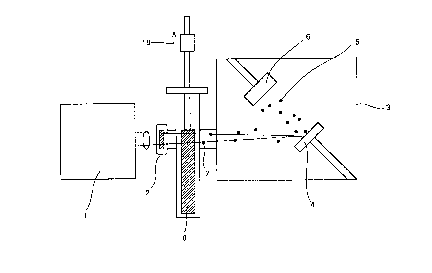
manufacturing apparatus shown in Fig. 5, for example, is
employed in general. Referring to Fig. 5, this oxide
superconducting film manufacturing apparatus comprises a
laser oscillator l, and a thin film forming chamber 3
having a laser entrance window 2. This laser oscillator 1
is set in the exterior of the thin film forming chamber 3.
The thin film forming chamber 3 is provided therein with a
target 4 containing components of an oxide superconductor,
and a substrate 6 which is arranged to face the target 4.
The target 4 provided in the thin film forming
chamber 3 is irradiated with a laser beam which is emitted
from the laser oscillator 1, through the laser entrance
CA 02101286 1997-12-30
window 2. The target 4 contains components of an oxide
superconductor. Upon such irradiation with the laser
beam, particles S of the material forming the target 4 are
scattered from the target 4, to be deposited on the
substrate 6 which is arranged to face the target 4. Thus,
a thin film of the material forming the target 4 is
provided on the substrate 6.
In such formation of a superconducting film by laser
ablation method, however, the particles are scattered from
the target 4 not only toward the substrate 6 but toward
the laser entrance window 2 during film formation, to
adhere to the laser entrance window 2. Thus, laser
transmissivity of the laser entrance window 2 is so
reduced that power of the laser beam which is applied to
the target 4 is reduced with time. When the laser power
is thus reduced with time, it is impossible to obtain a
superconducting film having high characteristics.
Particularly in formation of a large area film such
as a tape wire, a long time is required for film formation
and hence the as-formed tape wire is irregularized in film
quality and film thickness along its longitudinal
direction due to the aforementioned reduction in laser
power with time. Thus, it is impossible to obtain an
oxide superconducting film having high and uniform
characteristics.
2 8 ~
SU~RY OF THE INVENTION
In order to address the aforementioned problem, an
object of the present invention is to provide an oxide
superconducting film manufacturing apparatus which can
prepare an oxide superconducting film having high and
uniform characteristics even if film formation takes a
long time.
According to a first aspect of the invention there is provided an
apparatus for manufacturing an oxide superconducting film employing
10 a laser ablation method. The apparatus includes a thin film forming
chamber having a laser-transparent laser entrance window, a target
situated in the chamber and containing components of an oxide
superconductor, a laser beam source for irradiating the target with a
laser beam from the exterior of the thin film forming chamber through
5 the laser entrance window, a movable laser-transparent plate provided
between the laser entrance window and the target and means for
controlling the power of the laser beam applied to the target at a
constant level thereby preventing the power of the laser beam being
applied to the target from reduction by contamination of the entrance
2 0 window caused by scattered particles. The control means rotates the
moveable laser-transparent plate while linearly moving the rotation
access of the plate.
2 8 ~
.
The movable laser-transparent plate may be provided in
the form of a sheet which is moved by a take-up supply.
In another aspect of the present invention, the
control means may preferably comprise detection means for
detecting intensity of light emission from a specific
luminous species contained in particles which are
scattered from the target during film formation, and means
for controlling the power of the laser beam emitted from
the laser beam source so that the intensity of light
emission from the luminous species is constant during film
formation in response to a light emission intensity
detection output received from the detection means.
Still another preferable example of the control means
may comprise first detection means for detecting intensity
of light emission from a specific luminous species
contained in particles scattered from the target during
film formation, means for controlling the power of the
laser beam emitted from the laser beam source so that the
intensity of light emission from the luminous species is
constant during film formation in response to a light
emission intensity detection output received from the
first detection means, second detection means for
detecting a control limit of the control means, and means
for moving the movable laser-transparent plate in response
to a detection output of the second detection means.
-- 6 --
,, ~
CA 02101286 1997-12-30
.
The movable laser-transparent plate may be linearly
moved, rotated, or rotated with linear movement of its
rotation axis. Further, the movable laser-transparent
plate may be provided in the form of a sheet which is
moved by a take-up supply.
A further preferable example of the control means may
comprise detection means for detecting intensity of light
emission from a specific luminous species contained in
particles which are scattered from the target during film
formation, means for controlling the power of the laser
beam emitted from the laser beam source so that the
intensity of light emission from the luminous species is
constant during film formation in response to a light
emission intensity detection output from the detection
means, and means for continuously moving the movable
laser-transparent plate during film formation.
The movable laser-transparent plate may be linearly
moved, rotated, or rotated with linear movement of its
rotation axis. Further, the movable laser-transparent
plate may be provided in the form of a sheet which is
moved by a take-up supply.
According to the present invention, the power of the
laser beam which is applied to the target is so controlled
at a constant level that the laser beam being applied to
the target is prevented from reduction in power by
contamination of the entrance window caused by particles
scattered during film formation. When the target is
irradiated with the laser beam which is at a constant
CA 02101286 1997-12-30
power level during film formation, a constant amount of
particles are scattered and deposited on the substrate,
whereby it is possible to obtain an oxide superconducting
film having high and uniform characteristics. Thus, the
present invention is remarkably effective for improving
superconductivity of a large-area oxide superconducting
film.
Further, the present invention is effective for
improving quality of an oxide superconducting film which
is formed at a high speed, whereby a particularly
excellent effect can be attained when the inventive
apparatus is applied to manufacturing of an oxide
superconducting wire which is obtained by employing an
elongated tape base material as a substrate and
continuously forming an oxide superconducting film
thereon, for example.
The foregoing and other objects, features, aspects
and advantages of the present invention will become more
apparent from the following detailed description of the
present invention when taken in conjunction with the
accompanying drawings.
CA 02101286 1997-12-30
DESCRIPTION OF THE PREFERRED EMBODIMENTS
(Embodiment l)
Fig. 1 illustrates an oxide superconducting film
manufacturing apparatus according to an embodiment of the
present invention.
Referring to Fig. 1, this oxide superconducting film
manufacturing apparatus comprises a laser oscillator 1,
and a thin film forming chamber 3 having a laser entrance
window 2. The thin film forming chamber 3 is provided
therein with a target 4 containing components of an oxide
superconductor, and a substrate 6 which is arranged to
face the target 4. Further, a laser-transparent plate 8
is provided between the laser entrance window 2 and the
target 4. The laser-transparent plate 8, which is in the
form of a rectangle, can be linearly moved along arrow 18.
The target 4 provided in the thin film forming
chamber 3 is irradiated with a laser beam which is emitted
from the laser oscillator 1 through the laser entrance
window 2. The target 4 contains components of an oxide
superconductor. Upon irradiation with the laser beam,
21012~
particles 5 of the material forming the target 4 are so
scattered that the material is deposited on the substrate
6 which is arranged to face the target 4. At this time,
the particles of the material forming the target 4 are
scattered not only toward the substrate 6 but toward the
laser entrance window 2. Such particles 7 being scattered
toward the laser entrance window 2 adhere to the laser-
transparent plate 8 before reaching the laser entrance
window 2. The power of the laser beam which is applied to
the target 4 is temporarily reduced by such adhesion of
the particles 7. When the laser-transparent plate 8 is
linearly moved along arrow 18, however, a clean surface
appears in a portion for transmitting the laser beam,
thereby recovering the laser power. Such movement of the
plate 8 is repeated during film formation. This movement
of the plate 8 may be controlled by a timer, or by
detecting reduction of the laser power.
Although the plate 8 is intermittently moved in the
aforementioned embodiment 1, this plate 8 may
alternatively be continuously moved during film formation
by reciprocation.
(Embodiment 2)
Fig. 2 illustrates an oxide superconducting film
manufacturing apparatus according to another embodiment of
the present invention.
-- 10 --
2iO12~
Referring to Fig. 2, this oxide superconducting film
manufacturing apparatus comprises a laser oscillator 1,
and a thin film forming chamber 3 having a laser entrance
window 2 as well as a target 4 and a substrate 6 arranged
therein, similarly to the embodiment 1. Further, a laser-
transparent plate 9 is provided between the laser entrance
window 2 and the target 4. The laser-transparent plate 9,
which is in the form of a disk, can be rotated along arrow
19 .
Similarly to the embodiment 1, the target 4 is
irradiated with a laser beam which is emitted from the
laser oscillator 1, whereby particles of the material
forming the target 4 are scattered not only toward the
substrate 6 but toward the laser entrance window 2. Such
particles 7 being scattered toward the laser entrance
window 2 adhere to the laser-transparent plate 9 before
reaching the laser entrance window 2. The power of the
laser beam which is applied to the target 4 is temporarily
reduced by such adhesion of the particles 7. When the
laser-transparent plate 9 is rotated along arrow 19,
however, a clean surface appears in a portion for
transmitting the laser beam, thereby recovering the laser
power. Such rotation of the plate 9 is intermittently
repeated during film formation. This rotation of the
plate 9 may be controlled by a timer, or by detecting
2101 28~
reduction of the laser power.
Although the plate 9 is intermittently rotated in the
aforementioned embodiment 2, this plate 9 may
alternatively be continuously rotated during film
formation.
(Embodiment 3)
Fig. 3 illustrates an oxide superconducting film
manufacturing apparatus according to still another
embodiment of the present invention.
Referring to Fig. 3, this oxide superconducting film
manufacturing apparatus comprises a laser oscillator 1,
and a thin film forming chamber 3 having a laser entrance
window 2 as well as a target 4 and a substrate 6 arranged
therein, similarly to the embodiment 1. Further, a laser-
transparent plate 39 is provided between the laser
entrance window 2 and the target 4. The laser-transparent
plate 39, which is in the form of a disk, can be rotated
along arrow 19 while its rotation axis 40 can be linearly
moved along arrow 29.
Similarly to the embodiment l, the target 4 is
irradiated with a laser beam which is emitted from the
laser oscillator 1, whereby particles of the material
forming the target 4 are scattered not only toward the
substrate 6 but toward the laser entrance window 2. Such
particles 7 being scattered toward the laser entrance
21~ 12~6
window 2 adhere to the laser-transparent plate 39 before
reaching the laser entrance window 2. The power of the
laser beam which is applied to the target 4 is temporarily
reduced by such adhesion of the particles 7. When the
laser-transparent plate 39 is rotated along arrow 19,
however, a clean surface appears in a portion for
transmitting the laser beam, thereby recovering the laser
power.
When the plate 39 is rotated by 360~ along arrow 19,
the rotation axis 40 of the plate 39 is linearly moved
along arrow 29 and thereafter the plate 39 is again
rotated. When the plate 39 is thus moved in combination
of rotation and linear movement, it is possible to
efficiently utilize the overall surface of the discoidal
plate 39. Such movement of the plate 39 is intermittently
repeated during film formation. This movement of the
plate 39 can be controlled by a timer, or by detecting
reduction of the laser power.
Although the plate 39 is intermittently moved in the
aforementioned embodiment 3, this plate 39 may
alternatively be intermittently moved during film
formation.
(Embodiment 4)
Fig. 4 illustrates an oxide superconducting film
manufacturing apparatus according to a further embodiment
21~12~;~
of the present invention.
Referring to Fig. 4, this oxide superconducting film
manufacturing apparatus comprises a laser oscillator 1,
and a thin film forming chamber 3 having a laser entrance
window 2 as well as a target 4 and a substrate 6 arranged
therein, similarly to the embodiment 1. Further, a laser-
transparent plate 10 is provided between the laser
entrance window 2 and the target 4. The laser-transparent
plate lO, which is made of sheet-type quartz, can be moved
along arrow 20 by a take-up supply 21.
Similarly to the embodiment 1, the target 4 is
irradiated with a laser beam which is emitted from the
laser oscillator 1, whereby particles of the material
forming the target 4 are scattered not only toward the
substrate 6 but toward the laser entrance window 2. Such
particles 7 being scattered toward the laser entrance
window 2 adhere to the laser-transparent plate 10 before
reaching the laser entrance window 2. The power of the
laser beam which is applied to the target 4 is temporarily
reduced by such adhesion of the particles 7. When the
laser-transparent plate 10 is moved by the take-up supply
21 along arrow 20, however, a clean surface appears in a
portion for transmitting the laser beam, whereby the laser
power is recovered. Such movement of the plate 10 is
intermittently repeated during film formation. This
- 14 -
2~128~
movement of the plate 10 may be controlled by a timer, or
by detecting reduction of the laser power.
Although the plate 10 is intermittently moved in the
aforementioned embodiment 4, this plate 10 may
alternatively be continuously moved during film formation.
((Experimental Example 1))
An oxide superconducting manufacturing apparatus
having a laser-transparent plate provided between a laser
entrance window and a target as in any of the
aforementioned embodiments was employed to form a
superconducting tape sample while continuously moving the
plate during film formation.
A substrate material was prepared from a flexible
tape of YSZ (yittria-stabilized-zirconia), which was
heated to a temperature of 700 to 750~C. A target was
prepared from a YlBazCu3O7 sintered body. A laser was
prepared from an excimer laser of 248 nm in wavelength
employing KrF as an excitation gas, with laser energy of
2.5 J/cm2 and a laser frequency of 40 Hz. A film forming
atmosphere was prepared from 200 mTorr of oxygen. The
tape substrate was carried to continuously form a film.
Fig. 6 shows distribution of characteristics along
the longitudinal direction of the as-obtained oxide
superconducting film. Referring to Fig. 6, the axis of
abscissas shows positions from a tape head and elapses of
21~2~
the film forming time, while the axis of ordinates shows
changes in film thickness and those in critical current
density (Jc) and critical current (Ic) at 77.3 K
respectively.
As clearly understood from Fig. 6, it was confirmed
that the film thickness, the critical current density Jc
and the critical current Ic were stable along the overall
length of the tape in the superconducting tape sample
which was formed by the oxide superconducting film
manufacturing apparatus having a mechanism for preventing
contamination of the laser entrance window.
((Comparative Example))
For the purpose of comparison, the conventional oxide
superconducting film manufacturing apparatus shown in Fig.
5 was employed to form a superconducting tape sample.
Other film forming conditions were similar to those
in Experimental Example 1.
Fig. 7 shows distribution of characteristics along
the longitudinal direction of the as-obtained oxide
superconducting film. Referring to Fig. 7, the axis of
abscissas show positions from a tape head and elapses of
film forming time, while the axis of ordinates shows
changes in film thickness and those in critical current
density Jc and critical current Ic at 77.3 K respectively.
As clearly understood from Fig. 7, it was confirmed
- 16 -
21~12~
that the film thickness, the critical current density Jc
and the critical current Ic were gradually reduced along
the longitudinal direction in the superconducting tape
sample which was obtained by the conventional apparatus
having no mechanism for preventing cont~min~tion of a
laser entrance window.
(Embodiment 5)
Fig. 8 shows an oxide superconducting film
manufacturing apparatus according to a further embodiment
of the present invention.
Referring to Fig. 8, this oxide superconducting
manufacturing apparatus comprises a laser oscillator 1,
and a thin film forming chamber 3 having a laser entrance
window 2. The thin film forming chamber 3 is provided
therein with a target 4 cont~ining components of an oxide
superconductor, and a substrate 6 which is arranged to
face the target 4. The superconducting film manufacturing
apparatus further comprises a camera 11 for catching light
emitted from scattered particles, a spectroscope 13 for
separating the as-caught light into its spectral
components, an optical fiber 12 connecting the camera 11
with the spectroscope 13, an amplifier 15 for amplifying
an input signal from the spectroscope 13, a computer 16
for transmitting a control signal so that intensity of
light emission is constant on the basis of the amplified
- 21~12~3~
signal, and a laser control computer 17 for controlling
laser power on the basis of the as-received control
signal.
The target 4 provided in the thin film forming
chamber 3 is irradiated with a laser beam which is emitted
from the laser oscillator 1 through a laser entrance
window 2. Upon irradiation with the laser beam, particles
5 of the material forming the target 4 are so scattered
that the material forming the target 4 is deposited on the
substrate 6 which is arranged to face the target 4. At
this time, the particles 5 scattered from the target 4 are
excited by the high-energy laser beam, to emit light
having a specific frequency. This light is caught by the
camera 11, and transmitted to the spectroscope 13 through
the optical fiber 12. The light which is separated in the
spectroscope 13 into its spectral components is converted
by a photoelectric element 14 to an electrical signal,
which in turn is amplified through the amplifier 15, so
that a signal of the spectral data is transmitted to the
computer 16. The computer 16, in which light emission
intensity Io from a determined luminous species in starting
of film formation is registered, transmits a signal to the
laser control computer 17 for controlling the as-received
light emission intensity I so that 0.8 ~ I ' 1.2 assuming
that Io = 1. On the basis of the as-received signal, the
- 18 -
21~128~
laser control computer 17 controls an applied voltage to
adjust the power of the laser beam emitted from the laser
oscillator 1.
((Experimental Example 2))
The oxide superconducting film manufacturing
apparatus according to the embodiment 5 was employed to
form a superconducting tape sample.
Other film forming conditions were similar to those
in Experimental Example 1. Yttrium oxide was employed as
a luminous species to be observed.
Table 1 shows changes over time in light emission
intensity from yttrium oxide contained in particles being
scattered from target in the film formed by the apparatus
according to the embodiment 5. The values of light
emission intensity were standardized assuming that the
level was 1 in starting of film formation.
Table 1
Elapsed Time (h.) Light Emission Intensity
of Yttrium Oxide
0
0.5 0.99
1.0 1.01
1.5 1.02
2.0 0-99
2.5 1.01
For the purpose of comparison, Table 2 shows changes
-- 19 --
210~286
over time in light emission intensity from yttrium oxide
contained in particles being scattered from target in a
film formed by the conventional oxide superconducting film
manufacturing apparatus as shown in Fig. 5.
Table 2
Elapsed Time (h.) Light Emission Intensity
of Yttrium Oxide
0
0.5 0.95
1.0 0.83
1.5 0.61
2.0 0.32
2.5 0.10
It is understood from Tables 1 and 2 that intensity
of light emission from yttrium oxide was stable regardless
of elapses of time in the sample manufactured by the oxide
superconducting film manufacturing apparatus according to
the embodiment 5. It is also understood that intensity of
light emission from yttrium oxide was gradually reduced
with time in the sample manufactured by the conventional
oxide superconducting film manufacturing apparatus.
Fig. 9 shows distribution of characteristics along
the longitudinal direction of the oxide superconducting
film formed by the oxide superconducting film
manufacturing apparatus according to the embodiment 5.
Referring to Fig. 9, the axis of abscissas shows positions
- 20 -
21~1286
from a tape head and elapses of film forming time, while
the axis of ordinates shows changes in film thickness and
those in critical current density Jc and critical current
Ic at 77.3 K respectively.
As clearly understood from Fig. 9, it was confirmed
that the film thickness, the critical current density Jc
and the critical current Ic were stable along the overall
length of the tape in the superconducting tape sample
manufactured by the oxide superconducting film
manufacturing apparatus according to the embodiment 5.
(Embodiment 6)
Fig. 10 illustrates an oxide superconducting film
manufacturing apparatus according to a further embodiment
of the present invention.
Referring to Fig. 10, this oxide superconducting film
manufacturing apparatus comprises a laser oscillator 1,
and a thin film forming chamber 3 having a laser entrance
window 2. The thin film forming chamber 3 is provided
therein with a target 4 containing components of an oxide
superconductor, and a substrate 6 which is arranged to
face the target 4. Further, a laser-transparent plate 8
is provided between the laser entrance window 2 and the
target 4. The laser-transparent plate 8, which is in the
form of a rectangle, can be linearly moved along arrow 18.
The superconducting film manufacturing apparatus further
- 21 -
21012~
comprises a camera 11 for catching light emitted from
scattered particles, a spectroscope 13 for separating the
as-caught light into its spectral components, an optical
fiber 12 connecting the camera 11 with the spectroscope
13, an amplifier 15 for amplifying an input signal, a
spectral data processing computer 22 for processing the
as-amplified signal, a main computer 23 for judging the
as-processed spectral data and transmitting a control
signal to a laser control computer 24 or a plate carrying
driver 25, and the laser control computer 24 for
controlling laser power and the plate carrying driver 25
for moving the plate 8 on the basis of the control signal.
In the oxide superconducting film manufacturing
apparatus having the aforementioned structure, automatic
control for bringing the laser power into a constant level
is carried out in the following manner. Fig. 11 shows a
flow chart of this automatic control.
The target 4 provided in the thin film forming
chamber 3 is irradiated with a laser beam which is emitted
from the laser oscillator 1 through the laser entrance
window 2. The target 4 contains components of an oxide
superconductor. Upon irradiation with the laser beam,
particles 5 of the material forming the target 4 are
scattered so that the material forming the target 4 is
deposited on the substrate 6 which is arranged to face the
- 22 -
2~312~6
target 4. At this time, the particles 5 scattered from
the target 4 are excited by the high-energy laser beam, to
emit light having a specific frequency. This light
emission is caught by the camera 11, and transmitted to
the spectroscope 13 through the optical fiber 12. The
light which is separated into its spectral components is
converted by a photoelectric element 14 to an electrical
signal, so that its spectral data is processed by the
spectral data processing computer 22 through the amplifier
15. Then, the spectral data is fed to the main computer
23, which in turn judges light emission intensity I from a
certain luminous species. When the light emission
intensity I is within a range of 0.8 ~ I ~ 1.2 assuming
that light emission intensity Io immediately after starting
of film formation is equal to 1, laser oscillation is
continued as such. When I > 1.2, the laser control
computer 24 adjusts the laser power so that the light
emission intensity I from the determined luminous species
is constant on the basis of the spectral data, to
thereafter continue laser oscillation. When I < 0.8, a
further judgement is made as to whether or not the laser
power is at the m~ximum. If the laser power is not at the
maximum, the laser control computer 24 adjusts the laser
power so that the light emission intensity I from the
determined luminous species is constant, to thereafter
21012~6
continue laser oscillation, similarly to the case of I >
1.2. When the laser power is at the m~X; mum, on the other
hand, the plate 8 is linearly moved by the plate carrying
driver 25. Thus, a clean surface appears in a portion for
transmitting the laser beam, to recover the laser power
and to thereafter continue laser oscillation.
Although the rectangular plate 8 is linearly moved in
the aforementioned embodiment 6, a discoidal plate such as
that shown in Fig. 2 may alternatively be rotated, or a
discoidal plate such as that shown in Fig. 3 may be
rotated with linear movement of its rotation axis.
Further, a sheet-type plate such as that shown in Fig. 4
may be moved by a take-up supply.
(Embodiment 7)
Fig. 12 illustrates an oxide superconducting film
manufacturing apparatus according to a further embodiment
of the present invention.
Referring to Fig. 12, this oxide superconducting film
manufacturing apparatus comprises a laser oscillator 1,
and a thin film forming chamber 3 having a laser entrance
window 2. The thin film forming chamber 3 is provided
therein with a target 4 containing components of an oxide
superconductor, and a substrate 6 which is arranged to
face the target 4. Further, a laser-transparent plate 8
is provided between the laser entrance window 2 and the
- 24 -
210128~
target 4. The laser-transmittance plate B, which is in
the form of a rectangle, can be reciprocated along arrow
26. The superconducting film manufacturing apparatus
further comprises a camera 11 for catching light emitted
from scattered particles, a spectroscope 13 for separating
the as-caught light into its spectral components, an
optical fiber 12 connecting the camera 11 with the
spectroscope 13, an amplifier 15 for amplifying an input
signal from the spectroscope 13, a computer 16 for
transmitting a control signal so that intensity of light
emission is constant on the basis of the amplified signal,
and a laser control computer 17 for controlling laser
power on the basis of the as-received control signal.
The target 4 provided in the thin film forming
chamber 3 is irradiated with a laser beam which is emitted
from the laser oscillator 1 through the laser entrance
window 2. Upon irradiation with the laser beam, particles
5 of the material forming the target 4 are scattered so
that the material forming the target 4 is deposited on the
substrate 6 which is arranged to face the target 4. At
this time, the particles scattered from the target 4 are
excited by the high energy laser beam, to emit light
having a specific frequency. This light emission is
caught by the camera 11, and transmitted to the
spectroscope 13 through the optical fiber 12. The light
- 25 -
21()12~6
separated into its spectral components is converted by a
photoelectric element 14 to an electrical signal, which in
turn is amplified through the amplifier 15, so that a
signal of the spectral data is transmitted to the computer
16. The computer 16, in which light emission intensity Io
from a determined luminous species in starting of film
formation is registered, transmits a signal to the laser
control computer 17 for controlling the as-received light
emission intensity I so that 0.8 ' I ~ 1.2 assuming that Io
= 1. On the basis of the as-received signal, the laser
control computer 17 controls an applied voltage to adjust
the power of the laser beam which is emitted from the
laser oscillator 1.
On the other hand, particles 7 which are scattered
toward the laser entrance window 2 adhere to the laser-
transparent plate 8 before reaching the laser entrance
window 2. When the laser-transparent plate 8 is
continuously reciprocated along arrow 26 during film
formation, however, it is possible to considerably reduce
the speed of the particles 7 adhering to the plate 8, as
compared with that in a case with no such reciprocation.
Although the rectangular plate 8 is linearly moved in
the aforementioned embodiment 7, a discoidal plate such as
that shown in Fig. 2 may alternatively be rotated, or a
discoidal plate such as that shown in Fig. 3 may be
21~12~
rotated with linear movement of its rotation axis.
Further, a sheet-type plate such as that shown in Fig. 4
may be moved by a take-up supply.
Although the present invention has been described and
illustrated in detail, it is clearly understood that the
same is by way of illustration and example only and is not
to be taken by way of limitation, the spirit and scope of
the present invention being limited only by the terms of
the appended claims.
- 27 -