Note : Les descriptions sont présentées dans la langue officielle dans laquelle elles ont été soumises.
S93122
-- 1 --
21 04278
BACKGROUND OF THE INVENTION
1. Field of the Invention:
The present invention relates to an optical
integrated circuit applied to an optical data processor
such as an optical computer.
2. Description of the Related Art:
Recently, it becomes more important to
transmit and process informational data. Especially,
data transmission and data processing using light are
thought as an important technology because light can
travel fast. An optical integrated circuit is a kind
of device which processes information consisting of
light. The optical integrated circuit can be made
small by employing optical waveguides. Such optical
integrated circuits can be produced on a large scale by
utilizing semiconductor manufacturing processes, that
enable production of the optical integrated circuits at
low cost.
Light signals are processed in such an opti-
cal integrated circuit, and are finally converted into
electric signals. Referring to Figure 5, a light
detector of a conventional optical integrated circuit
is illustrated. Figure 5 schematically shows a cross
sectional view of an optical integrated circuit 39
having a light detector 38. A p-type region 32 doped
with p-type impurities is formed in a surface region of
an n-type silicon substrate 31. The p-type region 32
and the n-type silicon substrate 31 form a pn conjunc-
tion. An electrode 33 and an electrode 34 are respec-
tively connected with the p-type region 32 and the
,. c
S93122
2 1 04278
n-type silicon substrate 31. The light detector 38
consists of a part of the n-type silicon substrate 31,
the p-type region 32, the electrode 33 and the elec-
trode 34. A buffer layer 35 is formed on the n-type
silicon substrate 31. An optical waveguide 36 is
formed on the buffer layer 35 and the p-type region 32,
and the optical waveguide 36 is directly in contact
with the p-type region 32.
Light 37 travels in the optical waveguide 36.
When the light 37 reaches above the p-type region 32, a
part of the light 37 is absorbed by the p-type region
32. The light absorbed by the p-type region 32 is
converted into electric signals, and the electric
signals are detected through the electrode 33 and the
electrode 34.
In the optical integrated circuit 39 having
the light detector 38, light sensitivity of the light
detector 38 depends on the length l of the p-type
region 32. The length l must be long enough to receive
much of the light 37 so that the light detector 38 has
the sufficient light sensitivity for practical use,
for example, to obtain a sufficient signal. However,
as length l is elongated, the light detector 38 is
more influenced by stray light in the optical integrat-
ed circuit 39. Such stray light degrades a
signal-to-noise ratio of the light detector 38.
The present invention overcomes the above
mentioned shortcomings associated with the conventional
optical integrated circuit and provides an optical
integrated circuit having a light detector with high
-
-- 3 --
21 04278
sensitivity and good signal-to-noise ratio.
8UMNARY OF THE INVENTION
In one form, the optical integrated circuit of
this invention includes: a dielectric waveguide having at
least a waveguide layer for transmitting light in a first
direction, the light having a free-space wavelength ~; a
first reflector for reflecting the light in a substantial-
ly opposite direction to the first direction, the first
reflector being formed on an end face of the waveguide
layer; a grating coupler having a grating for diffracting
at least a part of the light in a second direction which
is different from the first direction, the grating coupler
being formed at a surface of the waveguide layer; at least
one light detector for detecting the diffracted light,
each of the at least one light detector being optically
connected with the dielectric waveguide; and, a second
reflector for reflecting the light toward the at least one
detector, the second reflector being formed above the
grating coupler. A period of the grating satisfies the
following equation:
A = -
where A is the period of the grating, and N is an
effective refractive index of the dielectric waveguide.
The grating coupler and all of the light
detectors may have substantially the same length along the
first direction, and the grating coupler may be provided
right above the at least one light detector. There may be
only one such light detector.
In another form, the optical integrated circuit
of this invention includes: a dielectric waveguide having
at least a waveguide layer for transmitting light in
- 3A- 2t 04278
first direction, the light having a free-space wavelength
~; a first reflector for reflecting the light in a sub-
stantially opposite direction to the first direction, the
first reflector being formed on an end face of the wave-
guide layer; a grating coupler having a grating for
diffracting at least a part of the light in a second
direction which is different from the first direction, the
grating coupler being formed at a surface of the waveguide
layer; and, at least one light detector for detecting the
diffracted light, each of the at least one light detector
being optically connected with the dielectric waveguide.
The dielectric layer further has a cladding layer, the
waveguide layer being formed on the cladding layer. A
period of the grating satisfies the following inequality:
1 1 N
< -- < 11
~ A ~ ~ ~
where ~ is the period of the grating, N is an effective
refractive index of the dielectric waveguide, and ~ is a
refractive index of the cladding layer.
The grating coupler may have a shorter length
along the first direction than all of the at least one
light detector, and may be provided right above the light
detectors. There may be only one such light detector.
In either form of the invention, the grating may
comprise a plurality of ridges and grooves, each of the
ridges and grooves having a rectangular cross-section and
having substantially the same width along the first
direction.
This and other advantages of the present
invention will become apparent to those skilled in the
S93122
2 1 04 2 78
art upon reading and understanding the following de-
tailed description with reference to the accompanying
figures.
BRIEF DESCRIPTION OF THE DRAWINGS
Figure 1 is a schematic cross sectional view
of an optical integrated circuit of the present inven-
tion in Example 1.
Figure 2 is an enlarged sectional view of a
grating coupler in the optical integrated circuit shown
in Figure 1.
Figures 3A through 3C are schematic cross
sectional views for illustrating a method for producing
the optical integrated circuit shown in Figure 1.
Figure 4 is a schematic cross sectional view
of an optical integrated circuit of the present inven-
tion in Example 2.
Figure 5 is a schematic cross sectional view
of an optical integrated circuit according to a conven-
tional technique.
DESCRIPTION OF THE PREFERRED EMBODIMENTS
Example l
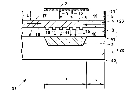
Figure 1 schematically shows a cross section-
al view of an optical integrated circuit 21 of the
present invention. A p-type region 2 doped with p-type
impurities is formed in a surface region of an n-type
S93122
-- 5 --
21 0427~
silicon substrate 1. The n-type silicon substrate 1
and the p-type region 2 are respectively connected
with electrodes 40 and 41, for example, shown for
convenience only as bold lines in Figure 1. A light
detector 22 consists of the p-type region 2, a part of
the n-type silicon substrate 1 and the electrodes 40
and 41. The p-type region 2 and the n-type silicon
substrate 1 form a pn junction for detecting light.
The light penetrates in the p-type region 2 and is
converted into an electric signal. The electric signal
is detected via the electrodes 40 and 41.
A lower cladding layer 3 made of silicon
dioxide is formed on the n-type silicon substrate 1. A
waveguide layer 4 made of silicon dioxide is formed on
the lower cladding layer 3, and an upper cladding layer
5 made of silicon dioxide is formed on the waveguide
layer 4. A dielectric slab waveguide 23 consists of
the lower cladding layer 3, the waveguide layer 4, and
the upper cladding layer 5. In this example, the
dielectric slab waveguide 23 is used as a dielectric
waveguide. The waveguide layer 4 transmits light 8 in
a first direction. A grating coupler 6 is formed at a
part of a lower surface 18 of the waveguide layer 4.
The grating coupler 6 is positioned above the p-type
region 2 so that lights 10, 11, 15, and 16 which are
diffracted in a second direction by the grating coupler
6 can irradiate the p-type region 2.
A first reflector 14 is formed on an end face
of the dielectric slab waveguide 23. As is shown in
Figure 1, light 13 traveling in the first direction is
reflected by the first reflector 14 and travels in an
S93122
-- 6
21 04278
opposite direction from the first direction. A second
reflector 7 is formed on the upper cladding layer 5.
The second reflector 7 is positioned so that lights 9
and 12, which are diffracted in an opposite direction
from the second direction by the grating coupler 6, can
be reflected in the second direction.
When the light 8 traveling in the waveguide
layer 4 reaches above the grating coupler 6, a part of
the light 8 is diffracted by the grating coupler 6 and
is divided into the lights 9 and 10. The light 9 is
diffracted toward the upper cladding layer 5 and the
light 10 is diffracted toward the lower cladding layer
3. The other part of the light 8, which is not dif-
fracted by the grating coupler 6, becomes the light13. The light 10 passes the lower cladding layer 3 and
irradiates the p-type region 2. The light 9 is re-
flected by the second reflector 7 and reaches the
grating coupler 6 again. A part of the light 9 passes
the grating coupler 6 without being diffracted and
becomes the light 11. The other part of the light 9 is
diffracted by the grating coupler 6 and is added to the
light 13. The light 11 passes the lower cladding layer
3 and irradiates the p-type region 2.
The light 13 is reflected by the first re-
flector 14 and reaches the grating coupler 6 again.
The light 13 is divided into the lights 12 and 15. The
light 15 passes the lower cladding layer 3 and irradi-
ates the p-type region 2. The light 12 is reflected by
the second reflector 7. A part of the light 12 passes
the grating coupler 6 without being diffracted and
becomes the light 16. The light 16 irradiates the
,~ ~
S93122
-- 7
21 04278
p-type region 2.
Figure 2 shows an enlarged cross sectional
view of the grating coupler 6. The grating coupler 6
has a grating which consists of a plurality of ridges A
and a plurality of grooves B. In order that the grat-
ing coupler 6 diffracts the lights 8 and 13 in a sub-
stantially perpendicular direction to the lights 8 and
13, it is preferable that a period ~ of the grating
substantially satisfies the following Equation (1).
Where, ~ is the free-space wavelength of the light
which travels the dielectric slab waveguide 23, and N
is the effective refractive index of the dielectric
slab waveguide 23. Moreover, it is further preferable
that the cross sections of ridge A and groove B are
rectangular and that the cross sectional width a of the
ridge A and the cross sectional width b of the groove B
are set to be same, as is shown in Figure 2. Such a
grating profile prevents second order diffraction light
from being generated at the grating coupler 6. Thus,
the light 8 and 13 can be diffracted in the perpendicu-
lar direction and irradiate the p-type region 2 effec-
tively. Moreover, a thickness c of the upper cladding
layer 5 is preferably selected so that the lights 10
and 11 have the same phase.
As is mentioned above, the light 13, which is
not diffracted by grating coupler 6, is reflected by
,
S93122
- 8 ~ 2104278
the first reflector 14 and reaches the grating coupler
6 again to be directed into the p-type region 2 of the
light detector 22. Therefore, most of the light 8
irradiates the p-type region 2 of the light detector 22
effectively. The lights 9 and 12, which are diffracted
in the opposite direction to the p-type region 2, are
reflected by the second reflector 7 and irradiate the
p-type region 2 of the light detector 22.
The optical integrated circuit 21 shown in
Figure 1 has the grating coupler 6 at the lower surface
18 of the waveguide layer 4. However, the grating
coupler 6 may be formed at an upper surface 17 of the
waveguide layer 4. At whichever surface the grating
coupler 6 is formed, the light 8 can be diffracted.
Diffraction efficiency of the grating coupler 6 is
different in accordance with the aforementioned posi-
tions of the grating coupler 6. Also, the diffraction
efficiency depends on the structure and materials of
the dielectric slab waveguide 23. Therefore, it is
preferable that the grating coupler 6 is formed at
either the upper surface 17 or the lower surface 18
which will have the higher diffraction efficiency.
Figure 1 shows that the light detector 22 is
formed near the first reflector 14. However, it is
also possible for the light detector 22 to be posi-
tioned relatively farther from the first reflector 14
formed on the end face of the dielectric slab waveguide
23. If the first reflector 14 is formed on the end
face of the dielectric slab waveguide 23, the light
which is not diffracted by the grating coupler 6 (i.e.,
the light 13) can be reflected by the first reflector
9 2 1 0 4 2 7~
14 and travel above the grating coupler 6 again. The
reflected light can also irradiate the p-type region 2
and increase the amount of the light which irradiates
the light detector 22. Therefore, relative to prior
light detectors, such as that shown in Figure 5, the
light detector 22 of the invention can have improved
sensitivity and signal-to-noise ratio without enlarging
the length l of the p-type region 2.
For the reason mentioned above, as is shown
in Figure 1, a distance m between the light detector
22 and the first reflector 14 can be selected in ac-
cordance with a structure of a device to which the
present invention is applied. However, in the case
where the attenuation of the light in the dielectric
slab waveguide 23 may not be neglected, the distance m
is preferably set to be in the range where the light
reflected by the first reflector 14 is not significant-
ly attenuated.
Hereinafter, a method for producing the
optical integrated circuit 21 will be described. The
optical integrated circuit 21 propagates the light
having a free-space wavelength equal to 780 nm by TEo
single mode.
As is shown in Figure 3A, p-type impurities
are doped in an n-type silicon substrate 1, and a
p-type region 2 is formed in a surface region of the
n-type silicon substrate 1. A lower cladding layer 3
(thickness: 2200 nm) is formed on the n-type silicon
substrate 1 by a sputtering method. The lower cladding
layer 3 is made of silicon dioxide and has a refractive
~, ~
S93122
-- 10 --
2 ~ 042 78
index equal to 1.45. After an electron beam sensitive
resist is co`ated over the n-type silicon substrate 1 by
a spin coat method, a resist pattern 27 having a grat-
ing pattern is formed by using electron beam
(Figure 3B). A dielectric slab waveguide 23 which will
be formed later is designed so as to have an effective
refractive index N equal to 1.506. According to the
Equation (1), a grating period ~ is calculated at
518 nm. Thus, widths d and e are set to be 259 nm
respectively.
As is shown in Figure 3B, the lower cladding
layer 3 is etched by 50 nm depth using the resist
pattern 27 as a mask. By using an anisotropic etching
method such as a dry etching, grooves D and ridges E
having rectangular cross sections are formed. After
the resist pattern 27 is removed, a waveguide layer 4
(thickness: 700 nm, refractive index: 1.54) is formed
on the lower cladding layer 3, as is shown in
Figure 3C. The waveguide layer 4 is deposited by a
sputtering method with a #7059 target which is commer-
cially available from Corning Company. A grating
coupler 6 is simultaneously formed at the lower surface 18
of the waveguide layer 4. The grating coupler 6 has a
grating consisting of ridges A and grooves B in accord-
ance with grooves D and the ridges E of the lower
cladding layer 3. Thus, widths a and b shown in Figure
2 are equal to 259 nm respectively. Then, an upper
cladding layer 5 (thickness: 2200 nm) shown in
Figure 3C is formed on the waveguide layer 4 by a sput-
tering method. The upper cladding layer 5 is made of
silicon dioxide and has a refractive index equal to
1.45. Whereby, the dielectric slab waveguide 23 con-
S93122
11 - 21 04278
sisting of the lower cladding layer 3, the waveguide
layer 4, and the upper cladding layer 5 is formed.
Then, as is shown in Figure 1, a first re-
flector 14 (thickness: 200 nm) made of an aluminum film
is formed on an end face of the dielectric slab wave-
guide 23. A second reflector 7 (thickness: 200 nm)
made of an aluminum film is formed on the upper clad-
ding layer 5 so that the second reflector 7 is posi-
tioned above the grating coupler 6. The first reflec-
tor 14 and the second reflector 7 are formed by a
vacuum evaporation method.
Example 2
Figure 4 schematically shows a cross section-
al view of an optical integrated circuit 24 of the
present invention. A p-type region 2 doped with p-type
impurities is formed in a surface region of an n-type
silicon substrate 1. The n-type silicon substrate 1
and the p-type region 2 are respectively connected with
electrodes 40 and 41, for example, shown for conven-
ience only as bold lines in Figure 4. A light detector
22 consists of the p-type region 2, a part of the
n-type silicon substrate 1, and the electrodes 40 and
41. The p-type region 2 and the n-type silicon sub-
strate 1 form a pn junction for detecting light, and
the light is converted into an electric signal. The
electric signal is detected via the electrodes 40 and
41.
A lower cladding layer 3 made of silicon
dioxide is formed on the n-type silicon substrate 1. A
waveguide layer 4 made of silicon dioxide is formed on
S93122
- 12 - 21 04278
the lower cladding layer 3. An upper cladding layer is
not formed on the waveguide layer 4 in this example.
However, an upper surface 17 of the waveguide layer 4 is
in contact with air 50. The air 50 functions as an
upper cladding layer because the air 50 has lower
refractive index than the waveguide layer 4. A dielec-
tric slab waveguide 25 consists of the waveguide layer
4 and the lower cladding layer 3. In this example, the
dielectric slab waveguide 25 is used as a dielectric
waveguide. The waveguide layer 4 transmits light 8 in
a first direction. A grating coupler 26 is formed at a
part of the upper surface 17 of the waveguide layer 4.
The grating coupler 26 ls positioned above the p-type
region 2 so that lights 10 and 15 which are diffracted
in a second direction by the grating coupler 26 can
irradiate the p-type region 2.
A first reflector 14 is formed at an end face
of the dielectric slab waveguide 25. As is shown in
Figure 4, light 13 traveling in the first direction is
reflected at the first reflector 14 and travels in an
opposite direction from the first direction.
The grating coupler 26 has a grating with a
period ~ . The period ~ substantially satisfies the
following Inequality (2).
~ ns ~ (2)
Where, /~ is the free-space wavelength of the light
which travels the dielectric slab waveguide 25, N is
S93122
- 13 -
21 04278
the effective refractive index of the dielectric slab
waveguide 25, and ns is the refractive index of the
lower cladding layer 3 which is contact with the wave-
guide layer 4.
In the case where the period~ of the grating
coupler 26 satisfies the Inequality (2), a diffraction
toward the air does not satisfy a phase matching condi-
tion, and light is diffracted only toward the lower
cladding layer 3 without generating second order dif-
fraction light. Therefore, when the light 8 reaches
the grating coupler 26, a part of the light 8 is dif-
fracted only toward the lower cladding layer 3 by the
grating coupler 26 and becomes light 10. The light 10
passes through the lower cladding layer 3 and irradi-
ates the p-type region 2. Light 13, which is not
diffracted by the grating coupler 26, is reflected by
the first reflector 14 and reaches the grating coupler
26 again. The light 13 is diffracted toward the lower
cladding layer 3 by the grating coupler 26 and becomes
light 15. The light 15 passes through the lower clad-
ding layer 3 and irradiates the p-type region 2.
As is mentioned above, by forming the grating
coupler 26 which satisfies the Inequality (2), the
light 8 is diffracted only toward the lower cladding
layer 3. Moreover, the light 13, which is not dif-
fracted by the grating coupler 26, can be reflected by
the first reflector 14 and reaches the grating coupler
26 again. Therefore, most of the light 8 irradiates
the p-type region 2 of the light detector 22 effective-
ly .
~.
S93122
- 14 -
21 04278
The optical integrated circuit 24 is produced
by the same method as is mentioned in Example 1. The
lower cladding layer 3 is made of silicon dioxide and
the waveguide layer 4 is formed by a sputtering method
with a #7059 target which is available from Corning
Company. Each layer has the same thickness and refrac-
tive index as is explained in Example 1. The dielec-
tric slab waveguide 25 has an effective refractive
index equal to 1.496. In order to determine a grating
period ~ of the grating coupler 26, by using the values
of the refractive index (1.45) of the lower cladding
layer 3, the effective refractive index (1.496) of the
dielectric slab waveguide 25, and the free-space wave-
length (780 nm) in the Inequality (2) the following
inequality is obtained.
264 (nm) < ~ < 312 (nm)
Thus, the grating period ~ of the grating coupler 26 is
set to be 300 nm.
The optical integrated circuit 24 shown in
Figure 4 has the grating coupler 26 at the upper sur-
face 17 of the waveguide layer 4. However, the grating
coupler 26 may be formed at an lower surface 18 of the
waveguide layer 4. At whichever surface the grating
coupler 26 is formed, the light 8 can be diffracted. A
diffraction efficiency of the grating coupler 26 is
different in accordance with an aforementioned position
of the grating coupler 26. Also, the diffraction
efficiency depends on the structure and materials of
the dielectric slab waveguide 25. Therefore, it is
preferable that the grating coupler 26 is formed at
S93122
- 15 -
21 04278
either the upper surface 17 or the lower surface 18
which will h`ave the higher diffraction efficiency.
Figure 4 shows that the light detector 22 is
formed near the first reflector 14. However, it also
is possible for the light detector 22 to be positioned
relatively farther from the first reflector 14 formed
on the end face of the dielectric slab waveguide 25.
If the first reflector 14 is formed on the end face of
the dielectric slab waveguide 25, the light which is
not diffracted by the grating coupler 26 (i.e., the
light 13) can be reflected by the first reflector 14
and travel above the grating coupler 26 again. Such a
reflected light can also irradiate the p-type region 2
and increase the amount of the light which irradiates
the light detector 22. Therefore, relative to prior
light detectors, such as that shown in Figure 5, the
light detector 22 of the present invention can have
improved sensitivity and signal-to-noise ratio without
enlarging the length l of the p-type region 2.
For the reason mentioned above, a distance m
between the light detector 22 and the first reflector
14 can be selected in accordance with a structure of a
device to which the present invention is applied.
However, in the case where the attenuation of the light
in the dielectric slab waveguide 25 may not be neglect-
ed, the distance m is preferably set to be in the range
which the light reflected by the first reflector 14 is
not significantly attenuated.
In the Examples 1 and 2, the light detector
using a silicon pn junction, a dielectric slab wave-
s~--
S93122
- 16 -
~t 04278
guide made of silicon dioxide, and first and second
reflectors made of aluminum are utilized. However, it
is obvious to those skilled in the art that aforemen-
tioned components can be modified according to the
wavelength of the light traveling in the optical inte-
grated circuit. For example, a light detector made of
indium gallium arsenide is suitable for detecting light
having the wavelength equal to 1.4 ,um. A dielectric
slab waveguide is used as a dielectric waveguide,
however, the dielectric waveguide may be formed in a
strip shape or in other shapes. Also, another metal
film such as a titanium film or a dielectric multilayer
film, such as a multilayer made of silicon dioxide and
titanium dioxide, can be utilized as a first or second
reflector.
In the Example l, the grating coupler 6 juts
out from the waveguide layer 4, however, the grating
coupler 6 may formed in hollows as is shown in Figure
4. Also, in the Example 2, the grating coupler 26
may jut out from the waveguide layer 4 as is show in
Figure 1.
Some exemplary values for indices of refrac-
tion and other dimensions are mentioned above. It will
be appreciated that other values which will enable
operation of the invention described may be used.
Various other modifications will be apparent
to and can be readily made by those skilled in the art
without departing from the scope and spirit of this
invention. Accordingly, it is not intended that the
scope of the claims appended hereto be limited to the
S93122
- 17 -
21 04278
description as set forth herein, but rather that the
claims be broadly construed.