Note : Les descriptions sont présentées dans la langue officielle dans laquelle elles ont été soumises.
21~7~
w,~s3/2o645 PCT/CA92/00135
TELEPHONE LINE INTERFACE CIRCUIT WIT~I VOLTAGE SWITCHING
Technical FiPl~ and Tn~ chio~
This invention relates to a line interface circuit for a t/ 1/ ~ . . line, in
particular a two-wire telephone subscriber line extending from a telephone central office or
S remote terrninal to a subscriber's telephone.
~ound ~rt
It is well known to provide a two-wire telephone line interface circuit in which the
outputs of a line driver circuit are coupled to the tip and ring wires of a telephone line via a
sensing circuit which is responsive to current on the wires. The sensing circuit enables
the hook status of the subscriber's telephone to be determined by monitoring the loop or
differential direct current on the wires, as well as providing a path for a.c. (e.g. voice)
signals to the telephone central office (C.O.). In order to provide for ringing signals to be
supplied to the line for activating a ringer of the subscriber~s telephone, generaDy cOntactc
of a ringing relay are provided on the output side of the line driver circuit, to connect the
tip and ring wires to ground and to a ringing voltage generator lc~l,~Liv~,ly and to
interrupt their to the line driver circuit outputs so that the line driver circuit is
not exposed to the high ringing voltage.
In such an ~ costs are reduced by sharing the ringing voltage generator
among many line interface circuits, but as a c - ~ a ringing voltage generator may
not always be " '~, available for supplying a ringing signal to a line when desired,
and the provision of different ringing signals (different rlc . or different ring signal
sequences) is ~ , ' ' Similar 1 g may be provided for other forms of high
voltage signaDing, such as coin and ssage waiting signaDing, with similar
L~val~L~
In Bolus et al. United States Patent No. 4,431,86~ issued February 14, 1984 and
entitled "Solid State Telephone Line Interface Circuit With Ringing Capability" there is
described a line interface circuit in which a low-level ringing reference signal can be
supplied to the input side of the line driver circuit to be arnplified thereby to produce the
desired high voltage ringing signal at the outputs of the lirle driver circuit, and at the same
time the supply voltage rails of the line driver circuit are controlled to follow (with an
offset) the values of the ringing signal waveform thereby to reduce power
dissipation in the line driver circuit. In this ~ ~ ~ a voltage generator for producing
the line driver circuit supply voltages is controlled in ~ upon the voltages sensecl
at the outputs of the line driver circuit.
With evolution of line interface circuits, and especially with increaC~ing numbers
and types of service (e.g. ringing r.c Lu~ . and sequences) being desired by andavailable to telephone s~bs~nb~c, it is becoming il~ c~ necessary to provide
21 05376
equipment such as line interface circuits which can be used in a versatile manner to
provide various features or services as these may be desired,
An object of this invention is to provide an improved line interface circuit.
Disclosure of the Invention
S According to one aspect of this invention there is provided an interface circuit for a
two-wire telephone line, comprising driver means for supplying direct current on the line,
a controlled voltage generator for generating a variable voltage, control means for
controlling the variable voltage generated by the voltage generator, and switching means
controlled by the control means for selectively supplying the variable voltage generated by
the volta~e generator either as a signalling voltage to at least one wire of the line or as the
supply voltage for the driver means.
Preferably the switching means is also arranged and controlled by the control
means for selectively supplying a source voltage as the supply voltage for the driver
means.
Thus the voltage generator can be used for both off-hook current iimiting and
supplying high voltage signals, such as ringing signals, to the line, and the supply voltage
for the driver means can be constituted by either the source voltage, which is typically a
CO. battery voltage, or the variable output voltage of the voltage generator. Power can
be conserved in the forrner case, occurring most of the time while the telephone line is not
in use (the on-hook state), by not achvating the voltage generator, and in the latter case by
controlling the output voltage of the voltage generator to limit off-hook current on the line.
The switching means uu..~, 'y comprises first to sixth switches respectively
for selectively connecting the source voltage to a supply voltage line of the driver means,
the variable voltage to the supply voltage line of the driver means, a first output of the
25 driver means to a first wire of the line, a second output of the driver means to a second
wire of the line, the variable voltage to the first wire of the line, and the variable voltage to
the second wire of the line. In preferred; " .1,l. . "~ ;. "-~. tbe third and fifth switches are
constituted by first and second contacts of a first relay~ the fourth and sixth switches aue
constituted by first and second contacts of a second relay, each relay has its second
30 contact phased oppositely to the first contact and includes a third contact having the same
phase as the first contact, and the third contacts of the two relays are connected in series
with one another and together constitute the second switch.
The interface circuit preferably includes means for monitoring direct current on the
line, the control means being arranged to control the variable voltage generated by the
35 voltage generator in ~p~Pn~lPn~P upon the monitored current when the valiable voltage is
supplied as the supply voltage for the dliver means. The control means is also desirably
arl-anged to control the switching means to supply the source voltage as the supply voltage
for the dliver means when the monitored cuurent is below a 1~ rl I l ~ 1 thleshold.
2 ~ 05376
Another aspect of this invention provides an interface circuit for a two-wire tele-
phone line, comprising driver means for supplying direct current on the line, a controlled
voltage generator for genelating a variable voltage, control means for controlling the
variable voltage generated by the voltage generator, and switching means controlled by the
5 control means for deriving a supply voltage for the driver means selectively from either
the controlled output voltage of the voltage generator or a source voltage.
Brief D~crr~ nn of the Draw;ngs
The invention will be further understood from the following description with
reference to the a~" . , i..g drawings, in which:
Fig. 1 is a block diagram illustrating a telephone line interface circuit in accordance
with this invention;
Fig. 2 illustrates a general forrn of a switching circuit of the line interface circuit of
Fig. 1;
Figs. 3 and 4 illustrate preferred forms of the switching circuit in two different
~ ."I.o.l;",~ of the invention; and
Fig. 5 is a flow chart illustrating operations of a control circuit of the line interface
circuit of Fig. 1.
Mode(s) of Carrying Out the Invention .
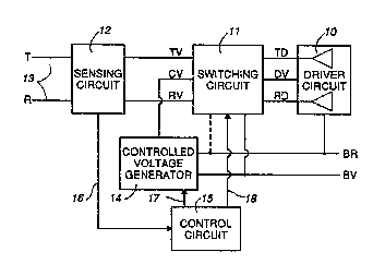
Referring to Fig. 1, there is illustrated a block diagram of a two-wire telephone
line interface circuit, which is typically part of a telephone central office or C.O (not
shown~. The line intelface circuit complises a line dliver circuit 10, a switching circuit 11
and a sensing circuit 12 via which outputs of the line driver circuit 10 are coupled to the
tip wire T and the ring wire R of a two-wire telephone line 13, a controlled voltage
generator 147 and a control circuit 15.
The line driver circuit 10 and the sensing circuit 12 can be of known form, for
example as described in Rosch et al. United States Patent No. 4,764,956 issued August
167 1988 and entitled "Active Impedance Line Feed Circuit77. Although not shown in
Fig. 17 receive path a.c. signals to be transmitted to the line 13 can be applied to an input
of the line driver circuit 107 and transmit path a.c. signals can be derived from the line 13
via the sensing circuit 127 in known manner.
The sensirlg circuit 12 provides on paths represented by a line 16 to the control
circuit 15 signals ~ wlLi..g the (d.c.) loop current7 which flows differentially in the tip
and ring wires and is supplied by the line dliver circuit 10 in known manner7 and common
mode current on the line 13. The control circuit 15 deterrrlines the sum and difference of
35 these currents thereby to determine the currents on the tip and ring wires individually,
monitors these currents and the loop cuulent signal as described further below7 and
provides control signals for the contlolled voltage generator 14 and the switching circuit
11 via colltrol paths 17 and 1~ lc~,~Li~e~y. Power for the controlled voltage generator 14
j~? 93/2064s 2 1 U 5 3 7 6 PCT/CA92/0013~
is supplied from a C.O. battery or other d.c. source Yia a battery voltage line BV (typically
48 volts) and a battery return line BR (ground or zero volts). The sensing circuit 12 and
control circuit 15 are also supplied with power derived from the battery via .,.which for clarity are not shown in Fig. 1.
S The controlled voltage generator 14 is a four-quadrant pulse width modulated d.c.
to d c. converter which can provide on a controlled voltage output line CV a voltage
which is controlled by the control circuit 15 via the control paths 17. This controlled
voltage can for example include a.c. and d.c. ~ r ' within a range f}om about -170
to about +180 volts peak, so that it can constitute various forms of high voltage signalling
used in telephony, such as ringing, coin, and message waiting signalling. The controlled
voltage generator (CVG) 14 can be enabled and disabled by the control circuit 15 as
further describtd below, and preferably has a high output impedance when it is disabled
or inactive.
The battery voltage line BV and the controlled voltage line CV are connected to the
switching circuit 11, which as described below can selectively connect either of these to a
driver voltage line DV which constitutes a supply voltage line for the line driver circuit 10.
The tip and ring drive outputs of the line driver circuit 10, lines TD and RD respectively,
are also connected to the switching circuit 11 which can connect them selectively, as fully
described below, to tip voltage and ring voltage lines TV and RV l.,~Liv~,l,y, which in
tum are coupled to the tip and ring wires T and R ~ ,Li~,l,y via the sensing circuit 12 in
known manner. The battery retum line BR is optionally also connected to the switching
circuit 11, as shown by a dashed line in Fig. 1.
Fig. 2 illustrates a general form of the switching circuit 11, which comprises
switches 21 to 28 which may be electro-mechanical switches, such as relay contacts, or
solid state switches, or a ~ ' of both. The switches 27 and 28, each having a
connection to the battery retum line BR which is only optionally connected to the
switching circuit l l, may likewise optionally be omitted and ~ vl,~ their c~ c
are shown in Fig. 2 by dashed lines. Each of the switches 21 to 28 is connected between
two connection lines of the switching circuit 11, as follows:
21 between BV and DV 22 between CV and DV
23 between TD and TV 24 between RD and RV
25 between CV and TV 26 between CV and RV
27 between BR and TV 28 between BR and RV.
The control circuit 15 controls the states of the switches 21 to 28, and the active
(enabled) or inactive (disabled) state of the CVG 14 as well as its output voltage when
active as described above, to provide various telephone operating conditions or modes
which are listed in Table 1 and are ' , 1~ described in detail. It is observed that
many other switch c~ ~ ..l . - - ;....~ are possible, but those in Table I represent a convenient
_ _ _ _ !
~93/20645 21~ ~ 3 ~ ~ pcr/cA92/ool3~
subset of c~mhin~n~nc for telephony operations. In Table 1, "C", "-", and "X" represent
IC~ ' closed, open, and "don't care" (i.e. open or closed) states of each switch,
"A" and ~r~ in the column headed "CVG" represent ~ ,ly active and inactive staoes
of the CVG 14, and the column headed "Application" indicates a typical telephony5 application for each respective operating mode:
Mode 21 22 23 24 25 26 27 28 CVG Application
C X C C ~ I Idle or d.c. feed
2 - C C C - - - - A Idle or d.c. feed
3 C - - C X - - - I Ground start
4 C - - C C - - - A Signalling on Tip
S X - - - C - - - A Coin signalling on Tip
6 C - C - - C - --= A Signalling on Ring
7 X - - - C C - - A Simplex coin signalling
8 X - - - C - -- C A Signalling on Tip
9 X - - - - C C - A Signalling on Ring
Table 1
It should be noted from Table I that in modes 5, 7, 8, and 9 the switch 22 is open
and the switch 21 can be open; the line driver circuit 10 does not need to be powered in
these modes of operation. When the CVG 14 is inactive, in modes 1 and 3, it is assumed
to present a high impedance at its output so that the switch 22 in mode 1 and 25 in mode 3
can be open or closed; if the CVG does not provide a high output impedance when
inactive these switches would have to be open in these modes.
In mode 1, the driver circuit 10 is supplied with the battery voltage and has its
outputs connected to the tip and ring voltage lines to result in a ~.u -~,..iU..dl
c~".r.~;...".;~." andtheCVGisinactive. Thismodeisgenerallyusedforthenormalon-
hook state of the line 13, which occurs most of the time, and enables a minimum amount
of power is used in this state.
In mode 2, the driver circuit 10 is supplied with the controlled voltage produced
by the CVG 14 instead of the battery voltage; this mode is adopted in the off-hook state of
the line 13. In mode 2, as described further below, the control circuit 15 monitors the
loop current signal supplied by the sensing circuit 12 via the line 16 and uses this to
determine the controlled voltage produced by the CVG 14, whereby a current limiting
operation is achieved to limit the loop current to a relatively low off-hook level, for
example of the order of 20 to 50 mA. Thus the controlled voltage which in this mode is
used to power the driver circuit 10 is adaptively adjusted to dCCOI.lll ' different loop
211)5376
WO 93/20645 6 PCT/CA92/00135~
resistances arising from diffcrent lengths of the line 13, thereby avoiding I ' 'y high
powGr ~ and dissipation which would otherwise arise due to high ~oop
currents flowing on short lines. Mode 2 can also be used as described further below to
C~ r ' for a low battery voltage.
S In mode 3, the driver circuit is powered from the battery voltage, and the switch
24 is closed to connect only the ring wr~e to its output, the tip wire being an open circuit,
thereby providing a ground start operating mode.
In each of the other modes 4 to 9, the control circuit 15 controls the CVG 14 togenerate a controlled voltage which, over time, has desired ~ for example
~ a ringing signal, a coin signal, a message waiting signal, or some other signal
which may have a relatively high voltage. Although the term "signal" is used for clarity rn
this respect, it should be appreciated that the CVG 14 can be used in this manner to supply
any desired voltage to either or both wires of the line, regardless of the specific purpose of
such voltage. Other purposes could include line testing (e.g. insulation testing) and line
5 C~J. 1;1 ;'~ ' ' 'D (e.g. "zapping" noisy lines) functions.
In mode 4, the switch 25 is closed so that this signal is supplied from the
controlled voltage line CV to the tip voltage line TV, and the switches 21 and 24 are
closGd so that the driver circuit 10 is powered from the battGry to provide a signalling
retum path via the ring drive line RD and this circuit 10. Mode 8 is similar except that the
switch 28 is closed, insoead of the switch 24, to provide a direct retum path via the battery
return line BR. Each of these modGs provides for signalling on the tip wire, with the ring
wire Orounded or at a pooential determined at the output of the driver circuit 10 on the ring
drive line RD. This potGntial rnay be determined to be anywhere bGtween the supply
voltages, e.g. -48 and zero volts, on the lines BV and BR ~ ,ly, depending on the
d c. conditions established for the driver circuit 10.
Conversdy, modes 6 and 9 provide for signalling on the ring wire with the tip
wire grounded (mode 9) or at a potential (mode 6) determined by the d.c. conditions of
the driver circuit 10. Thus in both of these modes the switch 26 is closed to supply the
controlled voltage from the line CV to the line RV. In modG 6 the switch 21 is closed so
that the driver circuit 10 is supplied from the battery voltage line BV and the switch 23 is
closed to connect the tip drive line TD to the tip voltage line TV; in mode 9 the switch 27
is closed to ground the tip voltage line TV. The controlled voltage on the line CV
produced by the CVG under the control of the control circuit 15 in this case may constitute
a ringing signal, of any desired frequency for frequency selective ringing and of any
desired ring signal sequence (e.g. long and/or short rings). It may alternatively constitute
a message waiting signal in the form of a 1 Hz pulse with a 50% duty cycle, or any other
dGsired form of signal which may bG of relatively high voltage.
W~93/2064S 2 1 ~ ~ 3 ~ ~ PCT/CA92/00135
In mode 5, the switch 25 is closed to connect the controlled voltage line CV to the
tip voltage line TV to provide for coin signalling on the tip wire with the ring wire open.
In mode 7 hhe switch 26 is also closed so that both of the lines TV and RV are connected
to the line CV to provide for the sarne signalling voltage to be applied to both of the tip
5 and ring wires, thereby providing for simplex coin signalling. In each of these modes the
driver circuit 10 need not be supplied with power, as already indicated.
As has already been indicated, the d.c. conditions at the outputs of the driver
crrcuit 10 can be controlled, by the control circuit 15, so that a desired potential is
provided on the lines TD and RD. More p~uh _' 'y, in modes 4 and 6 an ~I~U~ y
10 ground or zero volts potential can be estabiished on the lines RD and TD l~,U~Li~,ly~ so
tbat these modes include within their operating conditions modes 8 and 9 I~ "u._liv.,ly.
Accordingly, the switches 27 and 28 and the battery return line BR, shown in dashed
lines in hg. 2, need not be provided, thereby s;~ y;..g the switching circuit 11. Such
;.... is desirable especially in view of cost and reliability c~
It has been determined that, if the CVG 14 has a high output irnpedance when it is
inactive as discussed above, then the switches æ to 26 can be constituted by the contacts
of only two relays Kl and K2, arranged in either of two slightly different ways to provide
any of the operating modes 1 to 7. These two .... ~ are illustrated in Figs. 3 and
4 I~ ,Li~,ly, each individual ~ enabling six of the seven operating modes to
20 be provided.
Referring to Figs. 3 and 4, in each case the contacts of two latching relays Kl and
K2 are l~ .~l.t~l within dashed line boxes 31 and 32. The switch 21, shown within a
dashed line box 33, may .,u., v ~,..;~,..~y comprise a solid state (~ .. .. l... I ..l ) switch. The
switch 22 is effectively constituted by two series-coMected relay contacts 22a and æb.
one for each of the relays and hence in each of the boxes 31 and 32. Within the box 31
the relay contacts of the relay K 1 constitute the switches 22a, 23, and 25, and within the
box 32 the relay contacts of the relay K2 constitute the switches 22b, 24, and 26. Figs. 3
and 4 differ only in that the contact, " the switch 26 is connected to the line CV
directly in the ~ of Fig. 3 and via the switch 22a in the r ~ 1 l of Fig. 4.
In Figs. 3 and 4, the relay contacts of each relay are shown in what is referred to
as a reset state of the relay; for the relay Kl and box 31 the switches æa and 23 are clûsed
and the switch 25 is open (i.e. is oppositely phased), and for the relay K2 and box 32 the
switches æb and 24 are closed and the switch 26 is open (i.e. is oppositely phased). In a
set state of the relay Kl the switches æa and 23 are open and the switch 25 is closed, and
in a set state of the relay K2 the switches 22b and 24 are open and the switch 26 is closed.
Non-latching relays may ~' v.,1~ be used.
Table 2 below shows, for the ~ of Figs. 3 and 4 and for the operating
modes 1 to 7 discussed above, the necessary states of the switch 21, the relays Kl and
... . . _ .
WO 93/206~5 2 10 ~ 3 7 ~ PCT/CA92/00135~
K2, and the CVG 14. In Table 2, "C" represents the closed state of the sv~itch ~1, "S"
and "R" represent lC~ the set and reset states of the relays Kl and K2, "-"
represents the open state of the switch 21, "A" and "I" in the columns headed "CVG"
represent ~ ~Liv~ active and inacive states of the CVG 14, and the "Application"5 column is as in Table 1:
Fi~.3 Fi~.4
Mode 21 Kl K2 CVG 21 Kl K2 CVG Application
C R R I C R R I Idleord.c. feed
2 - R R A - R R A Idle or d.c. feed
3 C S R I C S R I Ground start
4 C S R A C S R A Signalling on Tip
S ~ot Availa~le C S S A Coin signalling on Tip
6 C R ¦ S A C R S A Signalling on Ring
7 C S S A Not Available Simplex coin signalling
Table 2
It can be appreciated from the above description that either of the ~ g . .. ~ t~ of
10 Flgs. 3 and 4 can be used to provide the vast majority of signalling funcions which may
be desired of a line interface circuit, using a minimal number of switching c..., .
and hence with relative economy and reliability.
Referring again to Fig. 1, it will be recalled that the control circuit is supplied via
the line 16 with a signal l~ ,DCI~ the differential or loop current. The control circuit
can .u.,v. '~, be a digital control circuit or state machine, and a digital-to-analog
converter may be provided to convert this signal on the linc 16 into a digital form for the
control circuit 15. The control circuit can produce the desired value of the
voltage required of the CVG 14 as a digital output to the CVG on the paths 17, and can
provide binary control signals for the switch 21 and the relays K1 and K2 on the paths
18. By way of example, Fig. 5 shows a flow chart in accordance with which the control
circuit 15 may operate to select either the CVG 14 or the driver circuit 10 for conttolling
the CVG 14 and the switch 21 to supply DC feed to the line 13 in operating modes I and
2 as discussed above. In each of these modes the relays K1 and K2 are reset, as shown
in Table 2.
Referring to Fig. 5, in a decision block 36 the control circuit 15 determines
whether the loop current is greater than 13 mA, this being used as a decision for the hook
status for the subscriber line 13. Lf the answer is no, it is concluded that the line 13 is idle
and the subscriber's lelephone i~ on-hook. In a further decision block 38 it i ~ rl~t~ f~i
w~s3/2~645 ~ 1 0 s 3 ~ ~ pcr~cAs2/ool3~
whether the C.O. battery voltage is low; if not as is normally the case a result block 40 is
reached in which the control circuit 15 renders the CVG inactive and closes the switch 21
to use the battery for supplying the driver circuit 10 and hence the line 13. This produces
operating mode 1, which is a low-power state which prevails most of the time.
If in the decision block 38 it is determined that the battery voltage is low (the
control circuit 15 can monitor the C.O. battery voltage in any convenient manner), then a
result block 42 is reached in which the control circuit 15 opens the switch 21 and activates
the CVG to generate a fixed voltage, for exarnple 19 volts, for supplying the driver
circuit 10 and hence the line 13. This enables the line 13 to be supplied with a full d.c.
feed voltage even when the CO. battery voltage falls below this voltage, therebyprolonging desired operating conditions and improving reliability of operation. This
~,UlI~ lll~ tO operating mode 2.
If in the decision block 36 it is deter~nined that the loop current exceeds 13 mA.
then it is concluded that the subscriber's telephone is off-hook. Depending upon the
15 ætual loop current which is monitored by the control circuit 15, as lGIJlCDl~~l by a block
44 the control circuit calculates a desired output voltage of the CVG 14. This desired
output voltage may be deoermined so that the loop current is maintained at a relatively low
off-hook level, for example about 20 to 50 mA, thereby providing a loop current lirniting
function which enables power ~ . and dissipation to be maintained at relatively
low levels. In a subsecluent result block 46 the control circuit 15 opens the switch 21 and
activates the CVG to generate the desired voltage for supplying the driver circuit 10 and
hence the line 13. This also Cull~,~u..d~ to operating mode 2.
The steps r~ "f' ~I by the flow chart of Fig. 5 are carried out in a repeated
manner, along with other monitoring and control functions of the control circuit 15, so
25 that there is a continuing a~bilily and l~ UII~ of the control circuit to the prevailing conditions.
Although as described above the hook state of the line is used to determine, in the
absence of signalling such as ringing, whether the battery or the CVG 14 is used to
supply the driver circuit 10, a more . . ' ' .l. ~ can be made in order to
30 reduce, especially for long telephone lines, the overall power c. ~ , of the line
interface. Thus for example if the battery is able to supply a current of 20 mA to a long
line in the off-hook state, then it may be more efficient to supply the driver circuit 10 from
the battery voltage rather than from the CVG 14, because the latter necessarily operates at
less than 100% efficiency. For shorter lines which in the off-hook state would conduct
35 much higher currents if supplied with the battery voltage, it remains much more efficient
to activate the CVG 14 for supplying a ~ul~ lly lower supply voltage to the driver
circuit 10.
~105~76
WO 93/20645 PCT/CA92/0013
It should also be notsd that, as the sensing circuit 12 and the control circuit 15
provide for monitoring of the current on each of the tip and ring wires, the; ~ y
monitored currents can also be used in a feedback loop fo} controlling the CVG 14 to
reduce its output voltage and limit peak signalling currents so that they do not exceed
5 desired values. This current limiting can act as a safety measure for example for message
waiting signalling, and avoids high current flows on lines which may be ~,AC~;v~,ly
loaded with ringing equipment.