Note : Les descriptions sont présentées dans la langue officielle dans laquelle elles ont été soumises.
2~7~
Electron Lith~ dpl~y Usin~ a Photocathode
~ackground of the InYentivn
Te~hr~ ~eld
The field addressed concerns sub-micron imaging - imaging based on
S least dimensions of less ~an 0.3 ,um. A p~irnary objective is lithographic imaging in
the fabrication of Large Scale ~nt~.gr~tP.d circuils (LSI~.
Pl~esses of the inven~ion depend upon excitation of electrons from a
patterned photocathode by use of electrom~lgnedc radiation - generally radiation in
the ultraviolet spectram (of energies greater than Se~).
10 Description of the Prior Ar~
It is widely recognized that continlling mini~lri7~tion of LSI from
presently used 1.0-0.9 design rules will soon require a different approach to pattern
~lP.linezltion. Presently used radia~Lion in the near-UV spectrurn (~ _ 0.~0.5 ~m) is
considered wavelength-limiting. As now practiced, it is the general view that deep-
15 U~ will be sllbstit~lt~d~ in turn to be limiting at~ 0.25 ~m design rule.
Considerable work is directed to extension of UV to design rulesthought too small by the conventional view, Progress has been made on
development and use of phase masks. The prinçirle is phase c:lnrell~tinn of edge-
sca~ered radiation. Development of ~is approach is now at an advanced level to
20 accommodate variation in reference phase, e.g. due to p.~hllily effects for closely
spaced features, while co~ to produce the 180~ phase shift. It is expected that
use of phase masking will permit e~tf n~ion to clesign rules perhaps half as great as
the ~sumf~.d wavelength limit.
The realization that a different form of radiation will be required for
25 suçceeding LSI g~nerations - likely at the 256 mbit chip le~rel - is responsible for a
high level of ~ctivity worldwide.
World activity for the most part entails use of elec~oma~nPtic r~ tion
of shor~er wavelength - of soft x-ray. X-ray projection has proceeded apace with ~ ~:
experimental systems producing s:ltisf~ctory 0.1 ~Lm patterns (see, J. E Bjorkholm,
et al, J. Vac. Sci. Tech., v. ES8, p. 1509 (1990)). : ;
Electron imaging has not been overlooked. Evolu~ion of a mask ~ -
projection system gained from eY~eriP~nee in~he direct write Llect~on
Beam Exposure ~ystem (see, "B-beam Teehnology", Brewer, ed., chapter by J.
Trotel and B. Pay, pp. 325-33S (1980). SCattering with Angular T.imi~tion
35 Projection Electron-beam Lithography has been demonstrated in the forrn of
2 ~ ~ 7 ~
, .
- 2 -
reduction projection to yield a 0.1 llm design rule pattern. (See, S. D. Berger, et al,
J. Vac. Sci. Technol., B9 (6), p. 2996 (1991).)
Despite the obvious advantages of reduction projection - regarding cost
and fabrication of the mask - considerable effort is directed to 1:1 x-ray imaging
5 (see, G. K. Celler, et al, App. Phys. Lett., v. S9, p. 3105 (1991)~. There are many
who believe that increased maslc cost associated with 1:1 is offset by design
simplification and reduced apparatus cost relative to reduction projection.
~p~rimPntal systems have demonstrated feasibility of mask co~ u~ion and of
proximity printing at 0.2 llm design rule and smaller. Some believe that this
lO apploacll will be only a last resort. Mask fragility, always an issue, is aggravated by
the very close p~ h~ y required between mask and wafer. A major field of
endeavor is direc~ed to mask repair. The x-ray source eon~nues to be a problem - for
the most part effort is based on a synchrotron source, lLkely at a cost of at least ten
million dollars.
IS A now-abandoned effort of some years ago was based on use of a
photocathode. ln its most advance forrn, the photocathode, in replacing the mask,
was conct;~ d of a UV-transparent substrate, typically quartz, having one surface
coated by a patterned layer of a good photo emi~ter, for eY~mpl~7 cesium iodide, CsI.
The "blocking" ~egions were conc~it~lted of a poor photo-emitting m~Pri~l typically
20 ~ 'Ol~liUl~l (see, J. Vac. Sci. Technol. cited above). The structure was operated by
mini~tin~ the back surface with UV radiadon (ses, Trotel and Fay cited above).
Abandonment must be attributed to a number of drawbacks, some
regarded as inherent, some perhaps due to limitations in then-available conditions
and materials. For one thing the photoc~thnde itself was regarded as short-lived - as
25 needing frequent replacement. Recogni~ing that short life was likely due to
c~ ."~ ti~n - to reaction despite use of the best vacuum practically available - an
effort was apparen~ly made to seck out less reac~ive mS~teri~l Trotel and Fay at page
330 report the use of a noble metal - spe~itically of gold. The photoc~tho(le took the -~
fo~n of a very thin layer - of a SG A thick layer - to optimize needed surface
30 emission ~rom the highly absorbing gold layer. Ihe effort was un~lccescful - ~he
cathode did not last long hl operation and the apploach was ~b~n~lon~s!cl
Problems associatcd with design of the photocathode projec~ion sys~em
are discussed in IEEE Transactions on Elec~on Devices, vol. ED-22, No. 7, (July
1975~. Pirst char~ctf~ri7ing such systems as having excessive image distortion, the
35 author goes on to reach the conclusion that structural elevational differences on the
anode - on the image plane - may be signifîcant. Nllme~lly, the con~ si-n is
2~L0~
reached that achievement of * ().3 ~Im accuracy requires anode flalness of + 2 ~Atl~inment of smaller design rule patterns would presumably re~uire greater flatness.
A more recent article, J. Vac. Sci. Technol., B4(l), pp. 89-93, (Jan/Feb
1986), addresses future needs. On the assumption thal pattern area will be limiting,
S the authors firsl dismiss x-ray ~1ignment regis~ation marks as inadequate -
presumably as unduly space con~ in~ - and then suggest a step-and-repeat system
depending on back-scatter ~ nment marks. Acknowledging that the detection
system will not fimction in ~he presence of the high electric field required forresolution (for sufficiently short deBroglie wavelength~, provision is made for a
10 field-free region. Field-e.1imin~lti~n is the consequence of a movable grid placed at
the first m~gnptiG focus point - at the distance corresponding with the first 360~
cyclotron periosl. Of course, the ~l~sence of the grid, while of minirnal consequence
as so positioned, continues to be an imr~ mPnt and, in turn, requires signific~n~
apparatus/process complexity ~o avoid distortion of the image by the grid.
15 Summ~ry oî ~be Invention
A photocathode proiection system and its use in formation of submicron
images is described. The system may serve a number of objectives. It may serve as
a simple display. Use may be based on electron enhancing or discouraging, e.g. to
result in selective crystal growth as based on electron stimulated desorption. Most
20 significan~ near-term use is eYrect~d to take the form of submicron device
fabrication based on resist-p~ttPrning by the photocathode. While, as ~liscl1s~d in
the Detailed Description, the system may be based on reduction projection from alarge cathode pattern, first commercial use will likely be l:l. The following
description for cc,.lvenience is, unless otherwise stated, in terms of l: l device
~5 fahriça~ion enta~ling projection on an electron-sensitive resist-coated wafer.
Implicit ch~r~cten.~ti~s of such a systern are retained. The cathode
structure consists of a patterned coating of photoemissive materi~ on a W-
,~elll substrate. An inherent advantage is the good thermal conductivity of therelatively thick cathode structure. Thermal eYr~n~ion problems wi~ masks used in
30 tr~n~mi~sion systems both x-ray and electron - are 1e~np(l Ihe back surface of
the substrate is ~radiated by UV to emit imaged electrons from the p~ttçrnp~d
coating. Electrons are accelerated by an electric field in ~he direction of an anode
which may be at ~he image plane or beyond. A uni~orm rïlagnetic field between the
photocathode and the image plane, together with such a parallel electric a~celpr~tin~
35 field, results in cyclotron focusing on the image plane. (~athode-to-image separation
of from millimeters ~o centimeters corresponds with one or a ~ew cyclotron
2 ~
- 4 -
resonance periods from the emissive surface to the image plane.
Avoidance of the high space charge regions produced at cross-over in
conventional focusing systems permits operation in two regimes. In the high voltage
regime, e.g. 25 kV and above - 25 kV/em for the centimeter order of cathode-to-
wafer spacing contemplated - blurring due to random electron motion in the resist is
P~l In the low voltage regime, e.g. two or a few k~l - defined as the range
over which most of the electrons ~re absorbed wit-hin the resist - so that ~ew reach the
substrate - blurring due to back-scat~er of elec~rons from the substrate is avoided.
Choice of field values interrnediate the ~wo regimes may be appropriate.
The acknowledged prior art deficiency - short-lived photocathodes - is
addressed. It is agreed that a significant part of the problem is "cont~min:~tinn," and
that .~ nce of an appropriate vacuum level is difficult, if only because of
liberation of hydrocarbons or other co.~ rom the resist-coated wafer.
Consistent with an earlier appl~,~h, photoc~thodes oL the invention are of noble15 metal. Use of such low efficiency pholoe~ requires activation with photon
energies ~i~nifi-~ntly above the metal work function to, in turn, result in a large
energy spread for emitted electrons. Availability of large homogeneous m~nf~tic
fields, as resulting from use of sUpercon(luctin~ wire turns lessens the effec~ of the
energy spread. Cause of earlier failure of noble metal c~tho~es by pAor art workers
20 has not been id¢ntified. Exp~rimmt~lly, success has been realized with layer
ll~ic~ ~~esses of 100 A and greater, together with appropriate underlying rnateAal to
assure ~(lhPsil)n of the film. It is possible that earlier failures were due to
discontimlitips in the thinner (50 A) films repor~ed.
The concern with wafer smoothness by prior workers appears
25 unfounded. To some extent this may also be attributed to the rathe3r low nn~n~iç
field in1f :ncitif S (less than 1 tesla) used for focusing in the past. In any event, ~ere is
no such problem with magnetic focusing fields of frorn 2 to 10 tesla. Surface
roughness of of~-the-shelf silicon wafers with local elevation v~ tinn~ of 1 ~m has
no perceptible effect on resolution.
A .~i~nificslnt advantage of electron delin~ n is the inherent ability to
n ~netir~11y vary focal distance. An i~ nlive species takes advantage of this byproviding for ~m adjusting field. The large fields for filnd~ment~l focusing generally
depens~ on superconducting magnets. Easily controlled conventional sol~noi~c at or
near ~e focal plane may be used for fine focusing. A symme~ically shaped field
35 may be used for radially dependent aberrations. Local perturbations in field strength
as well as elevational changes on tile surface to be imaged as caused by prior
CA 021074~1 1998-04-14
.
- 5 -
processing of the wafer, may be addressed by independently controlled, small solenoids.
Charged particle delineation permits enlargement or reduction of the projected
image by adjustment of magnetic field intensity. While initial use is expected to be 1:1,
future use may incorporate reduction from a 4x-5x mask in the manner of x-ray and e-
5 beam projection systems. This may be accomplished by increasing field density in thedirection from the photoemitter to the wafer. Field compression to result in this image-
reducing "funnel" is particularly valuable for use with the photocathode of the invention,
but it may be applied more generally. It may even be reversed in direction to enlarge
the image.
X-ray stimulated fluorescent m~rkingc may provide both for registration of
succeeding processing steps, as usual in LSI manufacture, and for registration of
successive regions in step-and-repeat. X-ray is unaffected by the accelerating electric
field (the E-field) and so avoids need for a null-field region for this purpose. An
alternative alignment mechanism depends on electron emission from alignment paths on
15 the photocathode. Pads may be at corner positions and may generate characteristic x-ray
from correspondingly placed metal markers on the wafer. Proper selection of metal
composition differing from materials used in the device under construction avoids
confusion with any spurious emission.
In accordance with one aspect of the present invention there is provided method
20 for device fabrication ent~iling pattern delineationof minimum feature size smaller than
0.25 ~m, such delineation comprising irr~liating a resist with patterned electron
radiation, characterized in that such patterned radiation is yielded from a W excited
photocathode comprising free surface noble metal photoemissive material, in that said
radiation is focused on such resist as spaced an integral number of cyclotron resonance
25 periods from the photocathode, and in which focusing and electron acceleration result
from applied magnetic and electric fields of substantial uniformity across the entire cross-
section of patterned electron radiation.
In accordance with another aspect of the present invention there is provided
method for device fabrication ent~iling at least one projection electron im~ging step in
30 which the projected image is changed in size, characterized in that electrons in transit are
subjected to a magnetic field which is homogeneous in cross-sectional direction
orthogonal to transiting electrons, in that such field changes in cross-section at least once,
and in that change in image size accompanies such field change.
CA 021074~1 1998-04-14
i
- Sa-
Brief Description of the Drawings
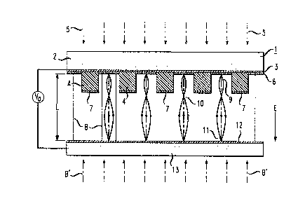
FIG. I is a diagrammatic view depicting a cathode structure of the invention
with provision for activation, electron emission, and cyclotron focusing. The cathode
structure shown is patterned by W-blocking regions below an overall emitting surface.
5 It is an example of a "thick-thin" cathode.
FIG. 2 depicts an alternative structure - a "thin-thin" cathode. Here,
photoemission is patterned by surface blocking regions of increasing work function.
FIG. 3 shows yet another different form of structure in which the photoemitting
material is, itself, patterned, with bared regions exposing underlying non-emitting
10 material. Reference is made to the drawing in discussion both of cathode
structures/materials and of processing.
FIG. 4 is a diagrammatic representation of a structure for "funnel" projection-
making using of ch~nging magnetic field density to reduce the size of the projected
image.
l S FIG. 5 is a diagrammatic representation of an alternative "funnel" structure.
! .. ~ ~.. .. . ' . ' . .. ' ' ' ' ' ' . ' . ~
2~7~5~
- 6 -
Detailed D~scrip~on
General
The essence of ~he invention has been described in the preceding
sections. Claims are directed to a process which does not show earlier difliculties in
5 photocathode patterning. Cathode st~uctures and operating parameters avoid critical
dependence on surface roughness and other impel~e-;lions. Multi-level processingand step-and-repeat, as well as continuous sC~nninc~ is expedited by use of the x-
ray-cxcited fiducial m~rking.~ described. Opfimal resolution may be assured by "fine
tuning" of magnetic field, preferably by use of a s~lpçrimposed smaller field which
10 rnay even be shaped to rectify local as well as systematic al~errations.
Available m~teri~ and procedures are adequate for described masl~
structures. The EBES direct write system, in worldwide use for mask fabrication,rnay be directly applied. Resist patterns, once defined and developed in usual
fashion, are then used in f~bri~tion of the photocathode. Deposition methods for15 contemplated mask m~ l.c are well-known.
Cathode StructurelMaterials
Inventive structures rely upon use of noble metal photoemitters.
Con~çm~ çd m~t~ri~l.c are element ~1 or allo~edl. While the inventive teaching may
be found useful for other types of m~teri~ls~ experimental support dictate~ exclusive
20 use of elemçnts numbers 44-47 and 75-79 of the Periodic Table according to
Mendeleev, i.e. Ru, Rh, Pd, Ag, Re, Os, Ir, Pt, Au, ax well as alloys of such
el~mf~n~. Selection is dictated by a variety of considerations. One is ease of
fo~Tnation - of for nafion likely of a thin layer atop a transparent substrate. ~till
another concerns ~eac~vity - on the basis of which Au is to be preferred over Ag, etc.
25 Another relates to work function. So, for e~mr,le, Au with its work function of ~
S. 1 eV (for its most favorable crystal plane) is, from this standpoint, preferred over
Pt with its work function of 5.6S or 5.7 eV. An initial advantage of Au is perrnitted
use of Pt masking with çxcit~ion intennediate the work functions of Au and Pt. As
a rule of thumb, the number of exiting electrons is proportional to the square of the
30 difference in energy between the work function and central frequency of the exciting
source e~yl~ssed as a percentage. Use of gold, with its lower work function, mayresult in a narrower energy sye~ 111! for emitted electrons.
Gold emitter material, however, rnay not be preferred for practical
reasons. Gold cont~n-in~tion of silicon may preclude f?~hri~tion of silicon devices.
35 Platinum, desplte its other disadvantages, for this reason may be preferred. F.~ mple
1 uses a Pt photocathode.
~ ':66 j j~ j;6 :~
2~a7~
- 7 -
Photoemitting naterials used ha~e short penetration slepths for exciting
energy. The noble metals have short UV penetration dep~hs. Emission probability
requires electron genera~ion close to the erni~ting surface. Practical con~i~ler~tions
suggest thick layers. Most effective emi.~,ic~n is a compromise bP~ween layer
S continuity and penetration depth. ~xpenment~l work supports a specified layer
thi~kn~ss range of from one hundred A to several hundred A - to 500 A or grcater.
Still greater thir~knpss is operative bu~ inefficient.
FIG. 1 shows a "thick-~hin" structure, 1. It is fabricated by depositin~
emitting material on the front surface of the cathode. Fmi~sil)n in blocking regions is
tO prevented by underlying material which absorbs andlor reflects exciting radiation.
Stlucture 1 consist~, of a substrate 2, which in the instance of an example, is
co~ ed of sapphire. Morc generally, the substrate ma~erial is chosen for
perforrnance properties including l-~r,~ ncy ~o the exciting radiation durability to
withstand handling, and thermal con.lu~;iivily ~o avoid thermal stress. The sapphi~e
15 substrate is coated with a thin - e.g. a 100 A - "glue" layer 3. Use of chromium
assures adherence and conti.luiLy of subsequent layered m:l~Pr~
It is found that adhesion is assured by use of "glue" mctals ~at ~orm
oxides with a heat of formation greater than that of SiO2. F~mrles are Al, Ti, Ta,
Cr. Ti, a particularly good adhesion promoter reduces SiO2 at relatively low
20 temperature and forms a strong bond. Metals such as Au, Pt, W and Mo do not
reduce SiO 2 - form oxldes with lower heat of formation than SiO 2. These mesalshave poor ~-lhf~cion to SiO2 and benefit by a "glue" layer. The structure shown is
f~bri~tPd by tirst coating the entirety of "glue" layer 3 with a layer of blocking
material 4 which is subsequently pattern ~lelin~ t~d to leave residual regions of
25 material 4. Regions, 4, serve to exdnguish - to absorb and/or to re~ect - exciting
radiation 5 and prevent excitation of overlying photoemissive m~t~ l. The
phols~e~.issive material is deposited after pattern delinea~ion to result in regions 6
and 7. In one example, gold serves as the material of regions 6 and 7. Thie~knes~ of
such regions is generally at leass 100 A, e.g. 250 A. In one eY~mI lP.7 blocking30 material ls tung~itf~n A 700 A tungsten layer is ~l~frlcielll to prevent ~ nifi-.an~
photoemici~iion from regions 7. The blocking material is chosen with ~,ntion to
requisite ~lh~.~inn tO underlying sur~ace - to "glue" layer 3 - and to requisiteadhesion ~or overlying surface - ~or emissive mateAal 7.
An alternative structure, is based on use of a continuous layer of
35 photoemissive material, with blocking regions serving to prevenl emission from
uniformly irradiated emissive ms~tr.risll Deposited regions of non-emissive material
2~7'~ 1
on the front face of the emitting surface serve tO pattern emission. Since blocking
material may be of ~ickness comparable to ~at of the emitter layer, such structures
arc here referred to as "thin-thin." FIG. 2 illustrates such a structure.
The structure of FIG. 2 includes a transparent substrate 20 which, as in
S FIG. 1, may be sapphire. Emission is from exposed regions of layer 21, a noblemetal layer of thickness satisfying crite~ia set forth - assuring absorption of exciting
energy near the emitting surface and to reliably result in a void-free (a continuous)
layer. It has been ~ound extremely helpful, in ~he instance of gold photoçmittPr, to
include a "glue" layer ~2. A 10() A ~ick layer of cl~ iulll has been found effective
10 for use with a 250 A layer 21 of gold. Blocking regions 23, of higher work function
m~ l, serve to pa~tern delin~flte. 100 A thick Pt, over "glue" layer 24, - e.g~ over
a 100 A thick Cr layer, is effec~ive. Generally, while omission of ~e "glue" layer
may not preclude a continuous adherent layer of emissive m~t~.ri~l, structural ~ .
integrity, particularly for gold, is best assured by its use.
The structure of FIG. 3 is based on a photoemissive layer 32 which is
etch-~lelinPatP(I to reveal regions of underlying non-emitting layer 33. Layer 33 is
bonded ~o substrate 34 by means Or "glue" layer 35. The mat~rial of layers 32-35may be gold, plalinllm~ quartz and chromium, respectively.
photoçmic~cion, in accordance with the invention, is the exclusive
20 province of noble meeaVs. Reference to "noble metal" cathode, etc., however, is not
intended to restrict the emitting surface to one consi~ g exclusively of noble
met~ls. The emitting material may be admixed to produce either a homogeneous or
inhomogeneous surface. Any such ad~lition~l rn~aterial should not ''cont~min~te" or
in any way impair emission efficiency.
25 Processirlg Con(litinn~
Reference is made to FIG. 1 for descrip~on of operation. Irradiation 5
pea~s at a photon energy to excite the photoemitter. Effective emission requiresphoton energy in excess of the work function of the emitter - excess of a minimum
of perhaps 10%. At the same time it must not be so large as to cause significant30 emission from regions to be blocked. The thick-thin structure of FIG. 1 satisfies ~is
need simply by adequate extinction of ultraviolet. Ihe eriteria are prim3rily those of
ma~erial properdes and thir~f~e~ of the blocking layer. Provision of surface
blocking regions to prevent electron emission from uniformly excited emissive
m~te~l, as in the thin-thin structNre of FIG. 2, is again subject to material and
3s ~hickness criteria. Other stluctures may provide for uniform exci~ation of otherwise
unblocked regions of expo~d matenal - of emissive, and of non-emissive m~tPri~l
': 92~7ac~
Under these circ~-m~t~nce~; criteria a~e simply those of ~e relative work functions of
regions constituting emitting and non-emitting por~ons of ~he cathode.
Excitltion radiation may be passed through a filter tO assure a
reasonably narrow energy spread of emitted electrons, e.g. i 10%. While the use of
5 a large accelerating field lessens the effect, a spread in electron energies, as emitted,
e.g., corresponding with a spread in photon energies, results in a spread in focal
distance. A krypton lamp operating at a peak of 6.5 eV is effective in exciting Pt
with its 5.6 eV work function. Al~ a~ive sources are deul~liulll lamps pealcing at 7
eV and mercury lamps peaking at 6 eV. All are eY Imr~1~s of high pressure lamps
10 operating as pklsma discl~a,ge tubes.
For an a~pfol)licl~ excitation source, the energy spread of electrons 9
permits good ~esolution upon imposition of magnelic field B to bring these electrons
to focus periodically as a~ node 11. The B field is uniform across the ef~ecti~eelectron emission cross-section - across an area at least as large as the region to be
15 pat~erned on la~yer 12. B fields, to several tesla in intensity, are convenien~y
produced by use of a superconrl~lcting magnet. Superconducting solenoi~ to yielduniformity of better than 1% over a volume of 1,000 cm3 are easily sufficient for
con~PmE)l~ted image areas of a few cm2. The image plane is here shown as
corresponding with the surface of a resist layer 12 on top of silicon wafer 13. In
20 such in.C~nr.Ç, the well-known positive-tone resist, PMMA, is usefully employed.
Alternatives in~ g the negative tone resist, COP, may be used. An electrical
field, ~, produced by voltage source Va accelerates the electrons 9 to the desired
velocity. The m~gnit~lde of the accelerating voltages is a compromise between line
rPsollltion in ~e resist and .~me~rin~ due to back-scfl~tPrin~ from the underlying
25 substrate. Lower voltages ",illi",;,~ back~ ?,t~Pring Higher voltages minimi7P.
image sme~tin~ in the resis~, but at the same eime reduce absorption by the resist to
protluce more back-sc~ttering ~om ~e substrate. Choice for ~ LillIUlll
reisolllSion/conerast may depend on the nature of the pattern. As an example, contrast
loss due to back-sc~ttPring is aggravated by large, closely spaced features. ~loltages
30 from 2 kV-100 kV have been found useful under exre~im~nt~l conditions seit ~orth in
the F.lrs m~
FIG. 1 includes a diagrammatic l~pl~ise~ on of magnetic field B'.
Such an optional adjusting field may colTect for abeirrations in the intensity of the
magnetic field B, either regular or irregular, across the imaging surface of layer 12.
35 As discussed, this adjusting field, likely to be of maximum value of 2 kilogauss and
of either polarity, is con~eniently produced by one or more conventional wirewound
' ~ .
2~7~
- 10-
solenoids below wafer 13. Regular deviation from uniformity vf the B field may be
compellsated by a single-shapcsl field, possibly produced by a single solenoid.
A~errations in focal distance due to local perturbations, e.g. due to elevational
changes on the plane to be imaged may best be accommodated by separate m~gnPts
~or most ~lem~n~in~ opera~ion, fine adjustment for each mask level may
be desirable. Expected valiation in focal distance due to mPch~ni~l movement,
tvlllpe~ variations, etc. may be non-critical for less riem~nding processing, inwhich event fine focusing may be required only at startup each day.
Figure 1 schP.m~ti~lly represents an arr~n~emPnt in which distance I, is
10 set to focus the image on resist 12 which is one cyclotron resonance period spa~ed
from cathode 1. Use of a single-period spacing, corresponding with a distance of ~
0.2 cm (under conditions as used in the Examples3, is sufficient separation to reduce
~e likelihood of damage to the cathode. Still larger spacinge, cvrresponding with a
greater number of periods, perhaps with some degradation but still adequate
15 resolution, are attainable. This permitted spacing constitu~s one of the main advan~ages of the i~ ve approach relative to 1:1 x-ray.
Fields of from 2 ~o 5 tesla together with an accelerating voltage of from
2 kV to 100 kV provide~ ~or 500 A resolution or bettvr at the image plane.
~rc~PlPr~tion within ~he noted range for current density of 1 to 10 micro amperes per
20 square centimPtPr (1-10 IlA/cm23 yields a PMMA exposure ~ime of tens of seconds.
For the most part, description has been in terrns of inct~nt~n~pous
exposure ~rom a 1:1 mask. The approach offers advantages both for s-~nninvg, e.g.
step-and-repeat, and for image reduction, e.g. by use of a 4x-5x mask as employed in
prospective e-beam and x-ray pr~ection systems. Scanning of smaller sub-images
25 relaxes le.lu,~ lls on field l~niro~ ity both ~or m~ne~ic field and elec~c field.
The prior art problem arising from use of Gducial marks based on back-scat~rit-g is
avoided by use of x-ray-stimulated fluorescence. M;~rking,~, e.g. of 10- 8 cm2 area
are adequate and avoid need to alter c~ n-lition~ optimized for ~elin~til~n
FI&. 4 is a schem~tic represelltation of a "funnel" - means ~or
30 rcducing/enlarging the projected image relative to the photocathode. It includes a
photoca~ode 40, lLI~e that of FIG. 1, con~ in~ Of sapphire su~ssr;~te 41 provided
wi~ chromium "glue" layer 42, tungsten blocking regions 43 and l~yered regions 44
and 45. UV radi~tion 46 excites regions 44, and is preven~ed from excl~ng regions
45 by regions 43.
~ 2~7~
A superconducting magne~ of individual or series turns 47, 48 and 49
produces a uniform magnetic field of e.g. 2 tesla as represen~ed by field lines 50. A
second superconducting magnet composcd of windings 51, 52, 53, 54 and 55
compressP.s the magnetic field to reduce its cross-sectional area, as now represented
by field lines 56 and to increase its il-~nsily perhaps to 10 tesla. The now-reduced
image is projected on layer 57 supported by substra~ 58. An applied voltage, Y a,
e.g. of ~0 kV, makes structure 40 cathodic rela~ive to layer 57.
Most desilably, the direction of the accelerating field is parallel to the
magnetic field lines 50 and 56. ln the particular embodiment shown in F~G. 4,
10 apparatus complexity is lessened by providing for a field-free region - for an electric
field-free region - between electrically conducting gratings 59 and 60 which areh~lerconni~cted by shun~s 61. Other aî~n~m~nt~ may use a separate accelerating
field, of direction parallel to the m~nP.tic field lines7 between the gratings 59 and G0.
Pig. S shows a "funnel" with provision for accommodating radially-
15 dependent differences in electron path length in the region of m~gnPtir, fieldcompression. For illustration purposes, the ~lluclule shown is identical to that of
E~ig. 4 with the e~ception of the accelerating grids 89, 90 and 91 and associated
biasing. Increased path length for extremal electrons is eo.~.penc~ted by grids 89 and
90, so shaped as to be more closely spaced for greater distance from the central20 beam. This illcl~ases the accelerating field to offset increasing path length and
improve flatness of the focal plane. In this illll~tr;ltion, field-free regions are
m~in~in~d on either side of the compression reg~ion. Acceleration is restricted to
regions 74-91 and 89-90 by voltage sources Va and V' a, respectively.
The "funnel'l approach is best suited to imaging electrons of near-equal
25 energies. This is implicit in photor~thodir. im~ing Other ~onms of imaging may
penmit a narrow energy spread. The "funnel" may be useful in systems using
absorption-transparency masks. It is likely not useful for sr~t~rin~;-non-sc~t~ering
masking due to energy-reducing collisions which increase energy spread of the
electrons.
30 Examples
Example 1 - A thin-thin cathode is used fi~r 1:1 delineation. ~he photo-emittingmaterial is a 200 A thick elrment~ layer (of work function 5.6 eV). Blocking is
by regions of 200 A thick tlmgsten which oxidized to yield a 100 A YV2 03 layer.The work fimction of its oxide is 7.5 eV. The structure is similar to tbat of FIG. 2
35 and consists of a sapphire substrate of 0.1 ,um thi~nf~ with a 100 A Cr "glue" layer
assuring adherence both of the Pt and W.
2~7 ~al
- 12-
l he backside of the cathode is irradiated by a klypton lamp~ A 2 lesla
magnetic field of 10~3 uniformity is applied. ~e accelera~ing field is 50 kV/cm or
25 k~l for ~he 0.5 cm cathode-to-wafer separation. p~ttPmin~ of 300 A features in
PMMA over a wafer area of lOcm2 requires from 5 to 10 ~conds.
S Example 2 - A thick-thin structure as shown in FIa. 1 uses 200 A thick Pt for
photoPmis~ion and 1000 A thick W for blocking - for UV absorption and/or
reflection. A krypton lamp is used for excitation. Cathode-to-w~fer separation is 1.5
cm. A magnetic field of 4 tesla and an accelerating voltage of 70 kV results in a
PMM[A prin~ pattern of 200 A features in 20 sec.
10 Fl~rnp~~ 3 - The apparatus and conditions of Example 2, however, with cathode-to-
wafer separation of 0.1 cm and by use of an açcPl~r~tin~ voltage of 2 kV is used to
pattern 1500 A fea~es on a PMMA-coated silicon wafer which is surface sensitizedby exposure to silane. Exposure time of approxim:~tçly twenty seconds is adequate.
Example 4 - A cathode of the structure OI FIG. 3 uses a 0.1 mm thick sapphire
15 substrate bearing a 100 A chromium layer and a final 100 A pl~timlm layer. The
platinum is patterned by direct electron beam wri~ing ~by EBES) on PMMA
followed by development. The pattern is transferred to the pl~timlm layer by plasma
etching to bare chromium. The composiie surface is oxi~li7P.d to produce a 100 Alayer of Cr203. The pattern-deline~t~pd photocathode is then used under the
20 conditions of FY:~mrlP. 2 to produce a 200 A design rule pattern in PMMA.