Note : Les descriptions sont présentées dans la langue officielle dans laquelle elles ont été soumises.
..,.
21077 ~ 0 1
A Method of Yroduaing a Corrugated Hoard as well as
a Corrugated Hoard
The present invention refers to a method according to the
generic clause of patent claim 1 as well as to a corrugated
board according t:o the generic clause of claim 9.
In the structure of a corrugated board known from US-A-4 685
563, a full-area continuous shielding layer of uniform
thickness is provided in the interior of the structure.
The outer surfaces of the corrugated board are untreated
and free, respeci_ively.
In the structure of a corrugated board known from US-A-4 482
048, at least ons~ shielding, full-area layer is provided,
again in the interior of the structure. The outer surfaces
of the corrugated board are untreated.
In the case of a folding case consisting of corrugated
board, which is l~;nown from DE-B1-2 947 262, at least the
free side of the cover layer facing the interior has been
printed on with an aqueous emulsion having carbon particles
dispersed therein.
DE-A-3 214 940 discloses a sheeting material which has been
printed on with a network or latticework of intersecting
lines of conductive printing colour on one side thereof or
on both sides thereof. When kraft paper is used as a sheet-
ing material for the outer cover layer of a corrugated
board, the network is only printed on the outer surface
thereof; the sheeting material is transparent; in the case
of corrugated board, openings are provided which permit
looking through.
CA 02107710 2004-11-12
2
A full-area, uniform application of the shield means does
not only~necessitate a comparatively large amount and an un-
necessarily large amount of shielding material, but, due to
the shield means integrated in the interior of the corruga-
ted board structure, major problems may arise when the
layers are glued together as well as with respect to the
durability of the glued connection. A corrugated board which
has been treated in this way is difficult to dispose of. A
network printed as a shield means onto the outer surface of
a sheeting material is susceptible to damage and permits~in
its interspaces the transmission of charges or discharges to
corners, edges or tips located in these interspaces and be-
longing to the components to be protected.
The present invention is based on the task of providing a
method of the type mentioned at the beginning as well as a
corrugated board in the case of which a reduced amount of
shielding material will suffice to produce the desired
shielding effect, and which are of such a nature that they
permit disposal without any ecological hazards, and by means
of which it is still possible to achieve a high standard of
quality and security.
The present invention is directed to a method that solves the above posed
task,
namely a method of producing a corrugated board consisting of paperboard or
paper material and used for cases or for sheet materials for protecting
electrostatically endangered articles against electrostatic discharges and
electric
fields, comprising the steps of glueing at least one corrugated layer and at
least
one flat layer together and applying, prior to the glueing of said layers, a
shield
means containing carbon and/or graphite to the surtace of at least one layer
which will be located in the interior of the future corrugated board
structure,
characterized in that the shield means is applied as a layer comprising
interconnected layer components and intermediate interspaces occupying a
CA 02107710 2004-11-12
2a
certain area, and that the layers including the shield means between them are
glued together in the area of the interspaces.
The invention is also directed to a corrugated board which is used for cases
or
for sheet materials for protecting electrostatically endangered articles
against
electrostatic discharges and electric fields and which has a corrugated board
structure comprising at least one corrugated layer and at least one flat layer
interconnected by glueing, and further comprising a shield means containing
carbon and/or graphite and applied to the surface of at least one layer which
is
located in the interior of the corrugated board structure, characterized in
that the
shield means consists of interconnected layer components having formed
between them interspaces which occupy a certain area, and that the layers
including the shield means between them are glued together by an adhesive in
the area of said interspaces.
In the case of the method according to the present inven-
tion, the interior surface of at least one layer in the cor-
rugated board structure is provided with the shielding mate-
rial predominantly only in the area of the layer components.
The amount of shielding material used is thus reduced (up to
40%); the corrugated board can be disposed of and recycled
in an ecologically beneficial manner. Due to the fact that
"~ 2107710
no anti-adhesive: shielding material, or a substantially
reduced amount o~f anti-adhesive shielding material is pres-
ent in the interspaces, said interspaces can be used for
glueing the layers together. Surprisingly enough, it turns
out that sufficient shielding is achieved in spite of the
interspaces (Faraday's cage). In spite of the interior
shield means, a durable and firm adherence between the
layers is guaranteed. Due to the fact that the articles to
be protected (electronic components, explosive or higly in-
flammable substances, e.g. chemical substances) are separat-
ed from the shield means by the semi-insulator defined by
the layer(s), and are also locally separated from said
shield means, the risk of damage which may be caused to said
shield means as well as the risk of spark-over are elimi-
nated. The corrugated board produced in this way does not
differ from conventional corrugated board as far as its out-
ward appearance is concerned, and it can be dyed or provided
with an imprint in an arbitrary manner, or it can be im-
proved in some other way.
Notwithstanding the fact that a reduced amount of shielding
material is used, the corrugated board according to claim 9
guarantees a good shielding effect, it can be produced at a
reasonable price and i.t is adapted to be disposed of or re-
cycled in an ecologically beneficial manner. In the inter-
spaces, a firm and durable glued connection between the in-
dividual layers is effected, similar to the glued connection
existing in the case of conventional corrugated boards.
In the case of a special embodiment of the present method,
the interconnected layer components are applied such that
the interspaces are free towards the surface. The Faraday's
cage consisting ~of the layer components produces the neces-
sary shielding effect. The free interspaces can be used ex-
cellently for glueing the layers together.
21 077 1 0
In the case of an alternative, preferred embodiment, the
interspaces are covered by thinner layer components oc-
cupying a certain area. The thinner layer components, which
occupy a certain area, supplement the shielding effect pro-
duced by the thicker, interconnected layer components. In
spite of this faces, it is still possible to provide a firm
and durable gluedl connection because the adhesive will pen-
etrate through said thinner layer components. Due to the use
of these thinner layer components, the total amount of coat-
ing material usedl will be smaller than in the case of a
full-area application of material of uniform thickness. This
is advantageous with respect to disposal and recycling.
It will be particularly expedient, when the interconnected
layer components are printed on and compacted. In the course
of a plurality of printing processes, e.g. four to six
printing processes, a firm and solid pattern of intercon-
nected layer components will thus be formed. Thanks to the
compacting, the total thickness of the corrugated board will
not be increased.
A particularly expedient way of applying the thinner layer
components is an application by means of full-area printing,
spraying on, or spread-coating, said application being car-
ried out prior to and/or subsequent to the application of
the interconnected layer components. With respect to the
small amount of. coating material used, one printing process
will be sufficient, for reasons of safety two printing pro-
cesses may be per:Eormed as well. Subsequently, the shield
means will consist of an interconnected layer with raised
and receding layer components. In cases in which compacting
has been effected, the interconnected layer components have,
thanks to said compacting, approximately the same height as
the thinner layer components. Notwithstanding this, the ad-
hesive will still be able to penetrate the thinner layer
..-.
21 0 77 1 0 5 --
components so as to establish the glued connection.
In the case of an alternative embodiment, the shield means
is prefabricated as a web of material, a lattice, or a net,
and is then additionally incorporated when the layers are
glued together. This i.s advantageous from the point of view
of process engineering, since the web, the lattice, or the
net can be prefabricated on a different site, and, subse-
quently, it only has to be inserted into the corrugated
board machine.
This web of material can, in an expedient manner, also com-
prise interconnected solid layer components and intermediate
thinner layer components filling the interspaces, the glue-
ing being predominantly effected through said thinner layer
components.
In the case of an additional, important variation of the
present method, an exterior surface of at least one layer
has applied thereto a full-area, conducting coating, said
coating being provided in addition to at least one interior
shield means. The conducting coating takes care that elec-
trostatic charges will be discharged, whereby the shielding
effect of the shield means will be supported and improved.
Between said conducting coating and the shield means, paper
or paperboard material. is effective as a semi-insulator, and
this will improve the protective effect of the corrugated
board.
In the case of an embodiment of the corrugated board in
which the interspaces between the interconnected layer com-
ponents are covered with thinner layer components occupying
a certain area, the layers including the shield means be-
tween them are durably and firmly glued together in the area
of said thinner layer components. The thinner layer compo-
2~ a~~ ~ 0
vents enhance the shielding effect of the Faraday's cage
defined by the interconnected layer components.
It will be expedient to adjust the thickness and/or the
density of said thinner layer components such that the ad-
hesive by means of which the individual layers are glued
together will penetrate through said thinner layer compo-
nents and reliably produce its adhesive effect.
Lines, paths, rods, strips or individual areas as intercon-
nected layer components define an effective Faraday's cage
in the corrugated board, most expediently in the form of an
approximately regular pattern so as to guarantee a uniform
shielding effect. In this connection, it turned out to be
expedient, when t:he total area occupied by the interspaces
exceeds the total area occupied by the interconnected layer
components. This will considerably reduce the amount of ma-
terial required for the shield means.
When the interspaces define an approximately regular pattern
whose orientation is perpendicular to, or oblique to the
direction of wave crests of the corrugated layer, the maxi-
mum number of uniformly distributed glued points between the
individual layers will :be obtained.
The shield means <:an also be incorporated in and bonded to
the corrugated bo<ird in the form of a prefabricated web of
material comprising the interconnected layer components and
the free interspac:es or the thinner layer components filling
said interspaces, and this will not impair the adherence
between the layers connected by glueing. For this purpose,
it will be expedient to incorporate a carrier web to which
the shield means has previously been applied.
An excellent shielding effect, which provides efficient
210771 0 '
protection against damage to the shield means and which re-
liably causes a :rapid discharge of electrostatic charges,
will be achieved, when, in addition to at least one interior
shield means, a full-area coating of conducting material is
provided on the outer surface of the corrugated board struc-
ture.
Furthermore, it will be particularly expedient to provide a
sublimable corro:~ion inhibitor on, in, or below the conduct-
ing coating, said corrosion inhibitor being either applied
previously or admixed to the conducting material. The cor-
rosion inhibitor will evaporate throughout a long period of
time and will thus provide and additional protection against
corrosion for the metallic surfaces of the components to be
protected. The corrosion inhibitor uses the corrugated board
structure as a depot from which it will evaporate slowly. It
will be expedient:, when said corrosion inhibitor contains
polar, organic salts; vapours, which are set free from said
salts, will condense on metal surfaces and form mono-mole-
cular films, which wil:L inhibit the electrochemical proces-
ses resulting in corrosion.
The surface resistance of the shield means in the corrugated
board structure should expediently be less than 104 ohm/
square, preferably less than 101 ohm/square. The surface
resistance of they outer surface of the corrugated board
structure provided with the conducting material lies be-
tween 105 and 1012 ohm/square. According to the standard
CECC 00 0015/I, 1.991, the shield means is, consequently,
electrostatically shielding, whereas the conducting coating
is electrostatically canducting.
Embodiments of the subject matter of the invention are ex-
plained on the basis of the drawings. In the drawings, the
shield means and the canducting coating are shown exagger-
210771 0
atedly thick. In actual fact, however, they are~thinner and
they must be imagined to have partly penetrated into the
layers of the corrugated board structure.
Fig. 1 shows a cross-section through a corrugated board,
alternative or additive detail variations being
shown side by side,
Fig. 2 shows a cross-section through an additional embodi-
ment of a corrugated board,
Fig. 3 shows a cross-section through an additional embodi-
ment of a corrugated board,
Fig. 4 shows a top view in the line of sight II - II of
Fig. 1,
Fig. 5a - 5e show detail variations
Fig. 6 shows a perspective view of a folding case consist-
ing of a .corrugated board, and
Fig. 7 shows a perspective view of a sheet material
consisting of a corrugated board.
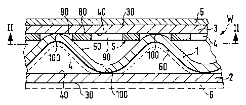
A corrugated board W according to Fig. 1, 2 and 3 is in-
tended to be used e.g. for producing cases, preferably fold-
ing cases F of the type shown e.g. in Fig. 6, or as sheet
material B accord_~ng to Fig. 7 used for packing articles,
such as electronic: components 10; these articles 10 are to
be protected against electric and/or electromagnetic and/or '
electrostatic dangers and possibly against corrosion.
According to Fig. 1, the corrugated board W consists of a
corrugated layer 7. which is glued to flat layers 2, 3 in the
.~-
21 0 7 7 1 0 9 __
area of its wave crests 100. Optionally, each of the layers
1, 2, 3 consists of several interconnected individual layers
of paper material or paperboard material. The simplest form
is an "open corrugated board" according to Fig. 3 comprising
only one flat layer 2 and one corrugated layer 1. Fig. 1 re-
presents the socalled standard corrugated board. The cor-
rugated board W according to Fig. 2 comprises two corrugated
layers 1 with an intermediate flat layer 2 and two flat lay-
ers 3 on the outer surfaces of the corrugated board struc-
ture.
In Fig. 1, the surfaces of the layers 3, 2 which are posi-
tioned in the interior of the corrugated board structure are
provided with reference numeral 40, whereas the exterior
surfaces are provided with reference numeral 30. The sur-
faces of the corrugated layer 1 provided with references
numerals 50 and 60 are located in the interior of the cor-
rugated board structure in Fig. 1. In Fig. 3, the surface 60
of the corrugated layer 1 is an exterior surface.
In Fig. 1, a shield means 4, which contains carbon and/or
graphite, is inserted between the layers 3, 1. The shield
means 4 consists of interconnected layer components 80 be-
tween which inte:rspaces 90 occupying a certain area are pro-
vided. The shield means 4 is applied to the surface 40 of
the layer 3. The interspaces 90 extend continuously up to
the surface 40. In the area of said interspaces 90, the cor-
rugated layer 1 is glued to the flat layer 3.
The shield means 4 may just as well be applied to surface 50
or - as indicated by the broken line - to surface 60 of the
corrugated layer 1. It is also imaginable to provide the
shield means 4 on surface 40 of the other layer 2. Further-
more, it is imaginable to provide a plurality of shield
means 4 in the corrugated board structure according to Fig.
1.
210771 0 10
The exterior surfaces 30 of layers 2, 3 in the corrugated
board W according to Fig. 1 can be untreated. It will, how-
ever, be expedient to apply to at least one of said surfaces
30 a continuous .coating 5 consisting of a conducting mate-
rial, e.g. a conducting lacquer. For the sake of simplicity,
such a conducting coating 6, e.g. in the form of an applied,
conducting lacquer, (indicated by a broken line), may also
be provided on t:he other surface 30 of the layer 2.
The shield means 4 is applied in several printing processes
for forming thus the interconnected layer components 80 and
for compacting said layer components. It will be expedient
to carry out up 'to six: printing processes with a printing
colour or aqueous emulsion containing carbon and/or graph-
ite, the area weight being 5 g/m2 (wet) corresponding to an
area weight of 2.5 g/m2 (dry) (these are, however, only
rough recommended values).
In the case of t:he corrugated board W according to Fig. 2,
at least one shield means 4 is provided in the interior of
the corrugated board structure. This shield means consists
of applied, interconnected, thicker layer components 80 de-
limiting interspaces 90, which are covered by thinner layer
components 90~. 'The application of said shield means 4 is
effected such that the thinner layer components 90~ are ap-
plied by full-area printing in one printing process, or two
printing processes at the most, of the surface of layer 2,
prior to the application of the interconnected layer com-
ponents 80 by printing, or that the interconnected layer
components 80 are first applied by printing, whereupon the
thinner layer components 90 are formed by subsequent full-
area printing. It is also imaginable to carry out one print-
ing process in which the thinner layer components 90 are
applied by full-area printing prior to as well as subsequent
to the printing processes for producing the interconnected
2107710 11
layer components 80 (e. g. three to four printing processes).
In the thinner layer components 90', it will be expedient to
adjust the application thickness such that said thinner
layer components 90' can be penetrated by the adhesive for
glueing the layers 1, 2.
In the corrugated board structure according to Fig. 2, the
shield means 4 may just as well be applied to one or to both
surfaces of a corrugated layer 1, or to the surface 40 of
one of the layers 3 or of both layers 3.
Preferably, but IlOt necessarily, one of the two surfaces 30
of the layers 3 has applied thereto a continuous conducting
coating 5, 6 consisting of a conducting material. Below said
coating 5, 6, or on top of, or within said coating 5, 6, a
sublimable corrosion inhibitor 12 (indicated by a broken
line) can be provided. In the case of the embodiment shown
in Fig. 2, a shield means 4 is applied to each of the sur-
faces 40 and 40' of the central layer 2.
In the case of the open corrugated board W according to Fig.
3, the shield means 4, which consists of interconnected
layer components 80 and of intermediate interspaces 90, is
provided between the layers 2 and 1. On the outer surface, a
conducting coating 5 is indicated. This conducting coating
may, alternative:Ly or additively, also be provided on the
free outer surface of the corrugated layer 1.
The shield means 4 according to Fig. 2, which comprises the
interconnected layer components 80 and the thinner layer
components 90' falling the interspaces 90, could just as
well be provided in the case of the corrugated boards ac-
cording to Fig. :l or Fig. 3. Vice versa, the shield means 4
of Fig. 1 comprising t:he free interspaces 90 may also be
provided in the corrugated board W according to Fig. 2.
21 0 77 1 0 12
In the case of each of the embodiments shown, the shield
means 4 may just as well be inserted with a web of material,
which comprises the interconnected layer components 80 as
well as the interspaces 90 and the thinner layer components
90', respectively, if necessary with the aid of a carrier
web (plastics sheet, paper or textile).
The total area occupied by the interspaces 90 and the thin-
ner layer components 90' is larger than the total area oc-
cupied by the interconnected layer components 80. The con-
ducting coating 5, 6 is applied to the respective surface
with a weight of approx. 25 to 30 g/m2 (wet). If a corrosion
inhibitor 12 is provided, said corrosion inhibitor will be
admixed e.g. to the conducting lacquer for the conducting
coating 5, 6 in a.n amount of 5 to 10 % by weight.
Fig. 4 is a schematic top view in the line of sight II - II
of Fig. 1 and corresponds to a view of the shield means 4 in
Fig. 2 or in Fig. 3. The interspaces 90 and the thinner
layer components 90' occupy a certain area and they are dis-
tributed comparatively uniformly such that they define a
pattern. The inte:rspaces 90 and the thinner layer components
90', respectively, are constructed and arranged in such a
way that the wave crests 100 of the corrugated layer 1 are,
at least in certain areas in the interspaces, either in
directed contact with the surface 40, or arranged in close,
opposite relatior.~ship therewith. The adhesive, which is not
shown, establishes a firmly adhering connection between the
layers 1, 3 or 1, 2. The glueing points are indicated by
arrows 110 in Fig. 4. It will be expedient when the pattern
of the interspaces 90 and of the thinner layer components -~
90' is oriented obliquely or perpendicularly to the orienta-
tion of the wave crests 100 so as to obtain the maximum num-
ber of uniformly distributed points of intersection between
the wave crests 1.00 and the interspaces 90 and the thinner
-.,
210771 0 13
layer components 90', respectively, at which glueing can be
effected.
The interspaces 90 and the thinner layer components 90' oc-
cupying a certain area can have any desired shape. It will
be expedient, when they are round, quadrangular or rhombic,
as indicated in l?ig. 4 and 5.
According to Fig. 5a, the shield means 4 consists of lines,
rods, paths, or :trips 120 and 130, which are applied such
that a network or latticework is defined and which cross one
another at right angles or at any other desired angle, said
lines, paths, rods or strips defining the interconnected
layer components 80. In the interspaces 90, the surface of
the layer to which the shield means 4 is applied is either
exposed, or the ithinner layer components 90' are provided,
which improve the shielding effect of the interconnected
layer components 80.
In Fig. 5b, various geometrical shapes for the interspaces
90 and the thinner layer components 90', which occupy a
certain area, arcs indicated, said geometrical shapes guar-
anteeing the largest possible number of points of inter-
section with the wave crests 100 of the corruagted layer 1.
The shield means 4 according to Fig. 5c consists of wavy
lines 140, which cross one another and which include the
interspaces 90 and the thinner layer components 90'.
In Fig. 5d, the interconnected layer components 80 are
approximately circular areas 150, which are interconnected
by cross connections 160 and which delimit the interspaces
90 and the thinner layer components 90'.
According to Fig. 5e, the interconnected layer components 80
are applied such that separate, approximately circular in-
" ~ 21 0 ~7 1 0 14
terspaces 90 or thinner layer components 90~ are included in
the shield means ~~.
If a shield means 4, which is constructed or applied in the
manner described hereinbefore, is applied to at least one
surface of a layer 1, 2, 3 located in the interior of the
corrugated board :structure, sufficient shielding will be
achieved by means of a comparatively small amount of shield-
ing material and the formation of long-lasting glueing
points between thEa individual layers will be possible.
The respective corrugated board structure has provided
therein at least one shield mens 4 with interconnected layer
components 80. If a full-area coating 5, 6 of conducting
material is additionally provided, said coating will be ap-
plied to at least one exterior surface.
If desired, a sublimable corrosion inhibitor 12 is provided
on, in, or below t:he conducting coating.
A folding case F consisting of a corrugated board W accord-
ing to Fig. 6 is a squared box comprising a bottom part 7
and a cover 8, which is adapted to be put over the opening
of said bottom part 7. The interior, which is identified by
reference numeral 9, serves to accommodate and protect at
least one electronic component, e.g. the article 10. The
surfaces of the falding case facing the interior 9 and, if
necessary, also the outer surfaces of the folding case have
been treated with a conducting coating 5, 6. Furthermore, a
printed image 11 c:an be provided on top of, or below the
coating 5, 6. If only one outer side of the corrugated board :"
W in the folding ease F is provided with a conducting coat-
ing, said coating should be applied to the outer surface of
the folding case B'. If only one shield means 4 is included
in the corrugated board structure, said shield means should
.....
210771 0 15
be positioned on the side of the corrugated layer 1 facing
away from the interior 9 because of the risk of punctures
from inside.
Fig. 7 shows a sheet material B which consists of the cor-
rugated board W according to one of the figures 1 to 3 and
which can be used for packing one or several articles 10, or
for producing blanks for folding cases F. The article 10 is
wrapped into the sheet material B, both outer surfaces of
said sheet material B being provided with a conducting coat-
ing 5, 6 in an expedient manner. If desired, a printed image
11 is applied as well, or the sheet material B bears an im-
print on one side or on both sides thereof.