Note : Les descriptions sont présentées dans la langue officielle dans laquelle elles ont été soumises.
~ ~ WO93/16492 ~ 1 0 8 ~ 4 2 PCT/US93/014XI
AD~ ~ CE ~ ~TI~ER ~OLDED PhASTIC PAC ~ GE
~SING MESIC TEC~NOLOGY
,
~3, BAC~GROUND OF T~ INVENTION
.,'j
FIELD OF ~EE INVENTION
The present invention relates to the field of electronic
packaging, particularly a method and resulting structure for a
high speed chip carrier.
''~
DESCRIPTON OF RELATED ART
. '~
High speed computers typically require minimal inductance
between the signal lines that link the integrated circuits (ICC)
of the system. The ICs are usually mounted into chip carriers
which have a plurality of leads that interconnect the chips and
the signal lines. The leads are typically parallel, which
creates an unacceptable amount of inductance between the leads,
particularly between the power and signal lines. This problem
becomes greater as the speed of the system increases.
U.S. Patent Nos. 4,891,687 and 4,835,120 issued to Mallik
et al, discloses an IC package that has a pair of copper plates
bonded to the lead frame of the package. The copper planes are
"
separated by insulative material and have tabs that are
connected to designated leads of the lead frame. The power and ~
ground pins of the IC are attached to each conductive plate ~-
respectively. Power flows into the ?ackage, from the leads, `
. '.
~ v ~
.~
. ,_~ W O 93/16492 2 10 3 .~ ~12 PCr/US93/014X1-~
;. 2
through the plates and into the IC. The creation of separate
power and ground planes eliminates the parallelism between the
leads, which reduces the inductance and increases the
capacltance of the signal lines. This reduction in impedance is
` particularly important for high speed circuitry.
~'~ Although the dual plane package reduces the noise within
the lines, the specific inductance and capacitance values are ~ -
somewhat unpredictable because of the size and tolerances
fi associated with the plates. Furthermore, there is no way of
connecting passive components to the lead frame to customi~e the
package. It would therefore be desirable to have an IC package
that would allow the designer to control the impedance and noise
of the circuit within the package. It would also be desirable
to have a method of constructing an IC package that can provide
internal routing with the package.
,,
. ..
::
~: ~
'.'''''~
.
~ ., ,:-.
~;
'`'"~: '
~,,,
. ~.
- 3 -
SUMMARY OF THE INVENTION
The present inventlon ls a method and resulting
structure for constructing an IC package. The package ha~ a
bottom conductlve plate havlng an lnsulatlve layer thereupon
ln a predetermlned pattern. Ad~acent to the lnsulatlve layer
ls a layer of conductlve metal thereupon. The layer of metal
can be lald down onto the lnsulatlve layer ln a predetermlned
pattern to create a power plane, a plurallty of slgnal llnes,
or a comblnatlon of power planes and signal llnes. On top of
the conductlve layer ls a lead frame whlch may be separated by
a second layer of lnsulatlve materlal. The second layer of
lnsulatlve materlal has a plurallty of holes fllled wlth a
conductlve materlal, whlch electrlcally couple the conductlve
layer wlth the leads of the lead frame. The power and ground
pads of the IC are attached to the conductlve layer and
conductlve plate, whlch are also coupled to correspondlng
leads of the lead frame, thereby connecting the IC to the
, ~ ~
leads of the lead frame. The slgnal pads of the IC are
connected to the lead frame and/or slgnal llnes formed wlthln
the conductlve layer. The IC and attached clrcult package can -
~then be encapsulated ln a plastlc shell as ls known ln the
art. The use of a thln fllm layer of lnsulatlve oxide
materlal may reduce the thlckness of the package, and lncrease
the dlelectrlc constant and resultlng capacltance of the
clrcult as well.
Addltlonally, reslstlve or capacltlve materlal
can be added between the slgnal llnes of the conductlve
-- 4
- layer, wherein resl~tors and capacltors are attached to the
-~ lndividual lines. The lnclusion of reslstors and capacitors
lnto the package provides a customlzed controlled llne
lmpedance over packages known ln the art. The present
inventlon also allows the creatlon of multlple layers and
~q
routlng wlthln the package, which 18 beneflclal for packages
wlth two or more ICs. The external routlng would allow
communicatlon between the multlple chlps wlthout havlng to
travel outslde of the package. The deslgner could thus deslgn
an lnflnite combinatlon of slgnal~ and power planes wlthln the
package ltself. The slgnal llnes of the present lnventlon may
be also spaced closer together, thereby allowlng lncreased pad
denslty on the IC.
The conductlve materlal between the conductlve
layers and lead frame ellmlnate the need for the attachment
tabs of the prlor art, whlch were cumbersome to produce and
assemble. The solldlfled conductlve materlal, commonly known
as vlas, also provlde more flexlblllty ln the deslgn of the
package, allowlng the deslgner to conflgure a varlety of
slgnal and power paths that wlll reduce the amount of nolse ln
the clrcult.
Accordlng to one aspect of the present lnventlon,
there 18 provlded an lntegrated clrcult package that houses an
lntegrated clrcult, comprlslng: a conductlve plate1 a flrst
lnsulatlve layer that ls ad~acent to sald conductlve platet a
'
~7 L
:
~: - s
flrst conductive layer that ls ad~acent to sald flrst
lnsulative layer; a second lnsulatlve layer that ls ad~acent
to sald flrst conductlve layer; a lead frame that 19 ad~acent
to sald second lnsulatlve layer, sald lead frame having a
plurallty of conductlve leads; at least one vla wlthln sald
second lnsulatlve layer that electrlcally couples sald flrst
conductlve layer to sald lead frame; and, flrst connector
means for electrlcally coupllng sald conductlve plate wlth
sald lead frame.
Accordlng to another aspect of the present ;
lnventlon, there ls provided an lntegrated circult package
that houses an lntegrated clrcult, comprlslng. a conductlve
plate; a flrst lnsulatlve layer that ls ad~acent to sald
conductlve platet a flrst conductlve layer that ls ad~acent to
sald flrst lnsulatlve layer; a second lnsulatlve layer that ls
ad~acent to sald flrst conductlve layer; a lead frame that ls
ad~acent to sald second lnsulatlve layer, sald lead frame
havlng a plurallty of conductlve leads~ at least one vla
withln sald second insulatlve layer that electrlcally couples
sald flrst conductlve layer to sald lead frame; and, flrst
connector means for electrlcally coupllng sald conductlve
plate wlth sald lead frame, whereln sald flrst connector means
lncludes at least one tab extendlng from sald conductlve
plate, that ls attached to sald lead frame.
~ '
.'~.
~ r
~ . ':'
~ - Sa -
.,
.. Accordlng to yet another aspect of the present
lnventlon, there ls provlded an lntegrated clrcult p~ckage
that houses an lntegrated clrcult, comprlslng, a conductlve
plate; a flrst lnsulatlve layer that ls ad~acent to sald
conductlve plate; a flrst conductlve layer that ls ad~acent to
sald flrst lnsulatlve layer; a second lnsulatlve layer that ls
ad~acent to sald flrst conductlve layer~ a lead frame that ls :~
ad~acent to sald second lnsulatlve layer, sald lead frame
having a plurality of conductlve leads; at least one vla ---
within said second insulative layer that electrlcally couples
sald flrst conductlve layer to ~ald lead frame; and, flrst
connector means for electrlcally coupllng sald conductlve - :
plate wlth sald lead frame, whereln sald flrst connector means
is at least one vla wlthln said flrst lnsulatlve layer that --
electrlcally couples sald conductlve plate to sald flrst
conductive layer.
Preferably thls lnventlon may provlde a method of
con~tructlng a chlp carrler that wlll allow lndlvldual slgnal
llnes to be lntegrally formed lnto the package structure.
Further, the present lnventlon preferably provldes a
method and resultlng chip carrler that has lntegrally formed
reslstors and capacltors connected to the slgnal llnes of the
package.
~',' '
...
,,~.
- 5b -
As well, the present lnventlon preferably provldeR a
chlp carrler that has power and signal llnes wlth a
predetermlned lmpedance value.
. .. ~
Also, the present lnventlon wlll preferably provlde
a chlp carrler that can be used wlth hlgh speed devlces.
Preferably, the present lnventlon wlll provlde a
chlp carrier that can lncrease the pad denslty of an IC.
,.~
Flnally, preferably the present lnventlon wlll .
provlde a chip carrler that can be constructed to have an
lnflnlte varlety of signal llnes and power planes.
'~
:.,
,~
b ~:
.. ....
',.~
: ~`...'`
:'.'~
W093/16492 ~ ~ O 8 5 ~ 2: 6 PCT/US93/0148
. ~--
:
The objects and advantages of the present invention will
become more readily apparent to those skilled in the art after
~ reviewing the following detailed description and accompanying
- drawings, wherein:
Figure 1 is a perspective view of a conductive plate;
Figure 2 is a side view showing a ceramic insulative layer
that had been vapor deposited onto the conductive plate of Fig.
1, wherein the insulative layer has holes;
Figure 3 is a side view showing the holes of the insulative
layer filled with conductive material;
Figure 4 is a side view showing a conductive layer that had
been vapor deposited to the ceramic layer of Fig. 2;
Figure 5 is a top view of Fig. 4, showing the circuitry
constructed on top of the insulative layer;
Figure 5a is a top enlarged view of a power plane of Fig. 5
showing the location of vias relative to the plane;
Figure 5b is a top enlarged view similar to Fig. 5a,
showing the vias electrically isolated from the power plane;
Figure 6 is a side view showing conductive material applied
at predetermined locations on the conductive layer of Fig. 4;
Figure 7 is a side view showing an insulative tape that is
attached to a lead frame, wherein the tape and lead frame have
holes formed therein;
Figure 8 is a side view showing the attached tape and lead
frame of Fig. 7 placed on top of the conductive layer of Fig. 6;
'r
, ~ , ... ... .
L~
~ 93/1~92 '~ PCT/US93/01481
,l . Figure 9 is a side view similar to Fig. 8, showing
conductive material inserted into the holes of the lead frame
and the insulative tape;
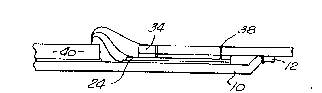
Figure 10 is a side view showing an assembled IC package of
the present invention;
,
Figure 11 lS a side view showing the assembled IC package
of Fig. 10 encapsulated by two plastic shells;
Figure 12 is a top view of the conductive layer, showing ~`
the incorporation of a thin film resistor connected to a signal
line;
Figure 13 is a side view similar to Fig. 10, showing the
resistor of Fig. 12 between the conductive layer and insulative
tape;
Figure 14 is a top view similar to Fig. 12, showing the -
incorporation of a thin film capacitor connected between two
signal lines.
:,. ' '~
~ " ~
~;
, .~ ~.
. , .
:,';",,~ ''''
,~ , , '"`;"'''.
::: .
. :.
,~
.:~
';.' ~:
' '' '.'
. , :
. ~, .,
Rere-= ng to the drawin~s more particular~y by refe~en~e
nu-..De-s~ Figure 1 shows a conduc_ive plate 10. The condUc~ e
pla=e 10 is pre re-ably Construc-ed from copper and may have tabs
12 formed at the ends as shown and desc_~ bed in ~ S Patent
Ncs. 4,8'5,120 and 4,891,687 issued to Malli~ et al.
As shown in Figure 2, a first layer 14 of insulatiVe
material is then vapor deposited onto the conductive
plate 10. The insulative material is preferably a
ce-amic such as aluminum oxide which can be vapor deposited with
techniques know in the art. The thickAes~ of the ce-amic 14 is
typically 5-15 mic-ons and has a dielectric constant of
approximately 7. In the preferred embodiment, a first laye~ 16
of nickel is vapor deposited onto the conductive plate 10 before
the ce:amic, so that the ceramic more readily adhe_es to the
plate 10. The nic~el 16 is typically 0.5 mic-ons thic.~ and has
an added func:ion of p~eventing metal migrat-on ac-oss the
ce-amic 14.
. .
As an alternate embodiment, a mas~ may be attached to the
conduc:ive plate 10, to prevent the deposition of ceramic onto
ce:.ain areas of the plate. After the oxide 14 is attached, the
ma ~ is removed, wherein there is ~ormed a plurality of holes ~8
in the ce_amic 14 as shown in Fig. 2. As ~hown in Figure 3, the
holes 18 are then filled with a metallic material 20 to create a
plurality of vias 22 through the insulati~e layer 14. The
metallic material 20 is pre_erably a silve- epoxy paste that
"flows" when elevated to a predetermined temperature and
solidifies when cooled down to room temperature. The via holeS
. .
.,
~ -'O93/16492 2 ~ ~ ~ 5 ~ 2 PCT/US93/01481
18 are typically 50 microns in diameter, but may be smaller or
larger depending upon the desired impedance characteristics of
the resulting circuitry.
As shown in Figure 4, a first layer 24 of conductive
material is vapor deposited onto the ceramic 14, wherein there
may be a second layer 26 of nickel deposited between the ceramic
14 and the conductive layer 24, to increase the adhesion of the
conductor 24 to the ceramic 14. The conductive material is
preferably copper approximately 5 microns thick. The copper may
be deposited such that a power plane is created on top of the
insulative layer 14. In the alternative, a mask may be attached
to the ceramic 14, to prevent the deposition of metal onto
predetermined areas of the insulative layer 14. After the metal
is attached, the mask is removed, whereby there is formed a
circuit that may have a plurality of slgnal lines and power
planes. The utilization of a mas~ with the vapor depositing
technique allows a designer to construct any pattern of signal
' .' :':
lines and power planes.
As shown in Figure 5, the circuit may have conductive -~
planes 28 separated from each other and from signal lines 30 ~ -
that run across the ceramic 14. If vias 22 are utilized, the
layer of metal 24 may be deposited on top of the vias 22 to
: .
directly couple the conductive plate 10 to the plane 28 as shown
in Figure 5a. As shown in Figure 5b, the second layer 24 could
be deposited so that the vias 22 are separated from the plane ~ :
28. This type of configuration allows the conductive planes 28
of the first conductive layer 24 to be electrically isolated
from the conductive plate 10, such that the plate 10 can be a
ground plane and the conductive planes 28 can be power planes.
,1 ~
/
~ ~ WO 93/1~92 2 i O ~ ~ 4 2 1~ PCTtUSg3/014~l ~
The vias 22 are then connected to pads 29 whlch provides
interconnection to a subsequent layer of conductive material.
- The ceramic and conductive layer is masked off so that the
- center 31 of the plate 10 is not covered by either material.
~- The exposed center section 31 allows a chip to be attached
.
directly to the plate 10. The process of depositing ceramic,
creating vias and depositing copper can be repeated to create a
plurality of conductive layers. Each layer may have a distinct
pattern of signal lines and power planes. The creation of
multiple layers is particularly useful when multiple ICs are
incorporated, wherein the various ICs can be interconnected
within the package.
As shown in Figure 6, after the top layer of conductive
j,
material 32 is deposited, balls of conductive material can be
applied to the conductive layer 24 in a predetermined pattern.
The conductive material is preferably silver epoxy paste as
described above. The paste can be applied with either a single
dispenser that sequentially places the balls, or the paste may
be applied with the use of a template that has holes
corresponding with the placement of the conductive material.
As shown in Figure 7 a second insulative layer 33 is
attached to a lead frame 34. The lead frame 34 has a plurality
;
of individual leads as is known in the art. The insulative
layer 33 is preferably a polyimide tape which has an adhesive
coating on both sides. Such a tape is sold under the trademark
KAPTON TM by E. I. du Pont de Numours & Co. The tape 33 and
lead frame 34 can be attached and trimmed per the method
disclosed in the Mallik patents. Holes 36 are drilled through
the lead frame 34 and tape 33 either before or after the
.
3/16492 ~ Jpcr~us93~014s~1
11
attachment cf the two members. The holes of the lead frame 34
can either be mechanically drilled or chemically etched. The
holes of the tape 33 can be chemically etched, or drilled with
either a laser or a mechanical drill.
As shown in Figure 8, the attached lead frame 34 and tape
33 is then placed on top of the first conductive layer 24, such
that the holes 36 are aligned with the conductive balls 32. -~
Conductive material 37 is then inserted into the holes 36, to ;
fill the holes 36 which creates a plurality of second vias 38,
as shown in Figure 9. The second vias 38 electrically couple
the leads of the lead frame 34 to the first conductive layer 24.
The assembly 40 is then heated until the conductive material and
adhesive on the KAPTON flows, whereby the adhesive attaches the
tape 33 to the lead frame 34 and the adjacent layers of copper -~
24 and ceramic 14. If the tabs 12 are incorporated into the
plate 10, the tabs 12 can also be pressure welded to the desired
leads of the lead frame 34. As an alternate embodiment, hole 36
can be formed in the tape 33 but not the lead frame 34. With
such an embodiment, the conductive balls 32 can be placed in the ;
holes 36 of the tape 33 after the tape 33 and lead frame 34 are
attached, but before the tape 33 is placed on the conductive ~-~
layer 24. The conductive balls 32 form vias that couple the
conductive layer 24 to the bottom surface of the leads.
As shown in Figure 10, a silicon die 40 incorporating an
integrated circuit can be mounted into the center section 31 of
the plate 10 and the pads of the die 40 can be wire bonded to
the corresponding leads 39, conductive layer 24 and plate 10.
The assembled die can then be encapsulated with a plastic shell
42, as shown in Figure 11, with methods known in the art. The
~ '
210~2
,W093/l649~ 12 PCT/US93/0148'--~
ground pads of the die 40 can be attached to the plate 10. The
plate 10 couples the ground pads to corresponding ground leads
- of the lead frame 34, either through the first 22 and second 38
vias, the tabs 12, or both depending upon the embodiment
employed. The power pads of the die 40 are electrically coupled
to corresponding power leads of the lead frame 34, through the
power planes 28 of the first conductive layer 24 and the second
vias 38. Likewise, the signal pads of the die 40 can be coupled
to the corresponding leads of the lead frame 34, through the
signal lines 30 in the first conductive layer 24 and the second
vias 38. The signal pads of the die 40 can also be connected
directly to the leads 34, as shown in Figure 10. Routing the
signal lines 30 through the first conductive layer 24 further
reduces the amount of crosstalk between the lines, because of
the short distances in which the lines are parallel with each
other.
Figure 12 shows an alternate embodiment, wherein a resistor
44 is connected to a signal line 30 to inerease the resistance
of the line. The resistor 44 can be created by vapor depositing
a resistive material such as nickel-chromium or tantalum
nitride, to the first conductive layer 24 before the tape 33 and
lead frame 34 are attached. The thickness of the vapor
deposited resistive material is typically in the range of 100-
5000 angstroms. In the alternative, a thick film of carbon can
be screened onto the signal lines to create the resistor 44.
The resistor 44 can be constructed to be in series with a signal
line, with two signal lines, or the resistor 44 may be parallel
with two lines, etc. The integration of the resistor 44 into
the IC package is more clearly shown in Figure 13. As shown in
~ '093/16492 13 210 ~ ~ ~ 2 PCT/US93/01481
Figure 14, a capacitor 96 can be created between two signal
lines 30. The capacitor 46 can be constructed by vapor
depositing a dielectric material such as tantalum oxide into the
space between the lines. Capacitors 46 can also be placed in
between two power planes in the first conductive layer 24. The ~-
present invention thus allows the circuit designer to customize -:
the circuit so that each signal line 30 and power plane 28 can
have a predetermined impedance. The addition of resistors 44
and capacitors 46 provides a more controllable manner of ~
establishing a predictable impedance value, which is ~ :
particularly important for high speed circuits.
While certain exempl~ry embodiments have been described in
detail and shown in the accompanying drawings, it is to be
understood that such embodiments are merely illustrative of and
not restrictive on the broad invention, and that this invention
not be limited to the specific constructions and arrangements
shown and described, since various other modifications may occur ~-
to those ordinarily skilled in the art. ~
'
, " :~
: ' ' ' ..
':- ' :"'
.
,.
' ';
',