Note : Les descriptions sont présentées dans la langue officielle dans laquelle elles ont été soumises.
r, 1
METHOD OF MANUFACTURING ELECTRICALLY CONDUCTIVE ~rFM~TS
PARTICULARLY EDM OR ECM ELECTRODES
Field of the Invention
This invention relates to a method of manufacturing
electrodes or other electrically conductive elements, and
particularly electrodes of complex shape, for example
10 electrodes for metalworking processes such as electrical
discharge machining (EDM) and electrochemical machining
(ECM).
15 Backqround of the Invention
Two most popular electro-mach;ning processes are
electrical discharge maç~ining (EDM) and electrochemical
mach;n;ng (ECM). Electrodes for EDM and ECM are themselves
20 usually ma~hine~ from conductive materials such as copper or
graphite. Since the shape of the electrode, or at least of
the working (active) portion thereof, must correspond to the
geometry of the EDM or ECM-machined part, the electrode
manufacturing process can be time consuming depending on the
25 complexity of the shape of the part. Thus far, complex
electrodes can take a number of days to manufacture, even
using numerically controlled (NC) marhines. A re~iew of known
techniques for the forming of EDM electrodes is given in a
paper by R. Gilmore, EDM Electrode Forming, Society of
30 Manu~acturing Engineers, Document MR9~-354 (1992), and also in
a paper by O. Rosenholm, Methods of Manufacturing Electrodes,
SME Document MR92-350 (1992). ~'~
During electrical discharge machining, electrodes are
subject to wear. Therefore, electrode life and cost are
~ ~87~'
significant factors in the ED~ processes. By comparison, ECM
processes do not cause any significant cathode wear since they
rely on electrochemical dissolution of the part being
machined. However, it is found frequently that the shape of
the part produced should be modified and so should be
correspondingly, the cathode. A modification of the cathode
could also be necessitated by disturh~ncps in the electrolyte
or variations in current density. In such cases, trial and
error methods are used to modify or remake the electrodes.
Even with the advent of computer aided design, measuring and
feedback te~hniques to assist in effecting the modifications,
the electrode machining still requires time, skill and
considerable care to carry out, and even the best systems
involve several iterations.
Summary of the Invention
According to the invention, there is provided a method of
manufacturing an electrically conductive element, the method
comprising the steps of:
providing a digital representation of at least a
working portion of the conductive element,
forming a three-dimensional solid replica of the~5 element or its portion from the digital representation, and
applying a layer of electrically conductive material
to at least a part of the replica.
In an embodiment of the invention, the replica of the
working portion of the element can be attached to a holder
before both the working portion and the holder are coated with
the electrically conductive layer.
The replicas can be produced by a number of rapid, tool-
less prototyping systems. An exemplary prototyping process
21~8 ~ ~? ~
. .
uses the capability of laser stereolithography to create a
three-dimensional solid model of a desired alement. It is
understandable that the computerized design can make allowance
for the thickness of the subsequent electrically conductive
~e.g. copper) layer.
The replica is typically made of an intermediate material
-n~hle to a tool-less prototyping method. Preferably, when
laser stereolithography is used, the material is a polymer or
another non-metallic, and non-conductive material.
The coating can be effected by electroplating, by
electroless plating or by other known processes, e.g. spraying
or evaporation.
Since the design of the final element is digitized, for
example, in a CAD file, it is a simple matter to modify the
representation, or design, rather than go through retooling
and prototyping process.
Brief ~escri~tion of the Drawinqs
'
In the drawings,
Fig. la shows a replica of the working portion of an
electrode,
Fig. lb shows the replica attached to a shank
(holder),
Fig. lc shows the replica and the shank plated with
copper;
Fig. 2 is a schematic representation of a
stereolithographic setup, and
Fig. 3 is a schematic representation of the steps of the -
present invention, showing an exemplary electrode produced by
the method of the invention and a product made therewith.
:
2 1 0 8 ~
Detailed Description of the Invent:ion
The invention combines certain known steps to arrive at
an unexpectedly advantageous result. It is known to pxoduce
digital representations of three~ n~ional objects as the
c~- ~Ler-aided des~gn, or CAD, has been in existence for a
number of years; rapid tool-less prototyping methods have
recently been developed; and electroplating/electroless
plating teçhni~ues axe also well known. However, the
combination of these techniques to arrive at a method for
manu~acturing electrodes, particularly ele~L o ~ - rh i n i ~g
electrodes of complicated ~h~e~, proves to be of significant
c~ ~rcial advantage when the estimated cost of the product of
the invention is compared with the cost of existing comparable
products. There is a long-felt want for inexpensive ECM and
EDM electrodes.
The digitizing o~ a desired shape, for example the
creation of cu~u~er aided designs, does not require detailed
explanation since the te~hnique is well known.
An exemplary tool-less rapid ~r ~Ly~ing process,
stereolithography, is described for instance by A.J. Lightman,
SAE Report 911115, Dayton, Ohio, 1991. A large part of the
paper is recited below.
The author states that modern ma~hi n; ng is done on
numerical control ma~hine~ which use computerized controllers
reading position and other sensors. The 3D CAD programs can
generate the numerical .~on~lol (NC) directives spPe~ing the
translation from design to product. Even with these modern
advances, the typical time required to go from design to
prototype is ~ces~ive.
The paper further states that almost all tool-less rapid
prototyping technologies, commercial or under development, use
2~Y7.~
the build-by-layer principle. The differences in the machines
are in the manner in which the layer information is presented
and the range of materials that can be used. Some systems use
the build-by-layer approach, while a few use a "free-form"
approach.
Regarding the "build-by-layer" approach, the concept is
to fabricate the part one layer at a time, attaching each
layer produced to those made before. In the end, a layercake
approximat~on to the desired part is produced. Adjusting the
lo layer thickness and the spatial resolution of each layer
allows the system to build the approximated part to the
desired degree of accuracy.
The layer information is derived from the CAD model. The
CAD model, being a 3-D representation, must include
descriptions of all the boundary surfaces and this description
needs to be in sufficient detail that there are no gaps
between joining surfaces. This description is either in the
form of a fully surfaced wire-frame model of the part or as a
solid model of the part. There are advantages and
disadvantages to each of these models and attempts are made to
form a hybrid CAD system co~bining the best features of the
two methods. Once the model is formed, it can be oriented in
the direction required for fabrication. Most fabrication
techni~ues have preferred directions providing best surface
finish or best accuracy (not necpc~rily the same direction).
The computer model is then intersected with the description of
a plane in a design space. The resulting intersection
provides the slice information for that plane. The plane of
intersection is moved from one end of the part to the opposite
e~ ?, in steps compatible with the fabrication techni~ue
and the complexity of the part. The steps do not have to be
constant; they can be varied within the machine's window of
capability, adjusted for accuracy or speed of fabrication
depen~ ng upon the local requirements. The slice files are
used to control the fa~rication process, building the part one
21~87!~i
layer at a time. There are a variety of specialized issues
for each process, related to the type of process, the method
of fabrication, and the ma~erials used. These need to be
considered before selecting a particular technology.
Laser Point-by-Point Fabrication
The most commonly employed technology (generically named
stereolithography) fabricates the layers by spot
polymerization of a liquid phot ~n~ er due to illumination by
a laser (W or visible). The laser is directed over the
surface of a liquid monomer pool (Fig. 2) on a path determined
from the layer information. The depth of polymerization
depends upon the laser energy deposited in the spot of
illumination. This is con~olled by moving the laser beam at
a speed detel i ne~ by its spot size and power, and the depth
of the slice set by the computer model.
The layer formed on the surface of the liquid must be
supported to maintain its position. Also it needs to be
tethered so that i~ does not move laterally, misregistering
the subsequent layers. A mechanical platform is often used
and the first layer is adhered to this platform. Once the
first layer is formed, new liquid photomonomer is in~L~d~ced
above it. This can be accompliche~ by lowering the platform
into the pool a distance correspon~;n~ to the thickness of the
next layer to be f~rmed or by keeping the platform stationary
and raising the level of the pool the required distance. Both
methods are used.
once a fresh layer of liquid of liquid photomonomer is in
place, the laser is directed to trace out the description of
the next layer. The laser speed is adjusted to polymerize the
desired depth plus an additional amount needed to adhere the
polymer to the layer beneath. This process is repeated until
the final layer is fabricated. The excess liquid is then
drained away from the solid, and the solid is cleaned and
~ 21~7~1
prepared for use by the designer.
Another technology operates using the same laser build-
by-layer basis. In this realization, the laser is used as a
heat source sintering the material. The process uses a
powder, rather than a liquid, typically a thermoplastic
although any material that can be thermally fused is a
candidate. The entire energy for the bonding must be
delivered by the laser (as opposed to initiating a chemical
reaction as in stereolithography). This requires a high-power
laser (Co2) even for thin layers of plastics. It does afford
the advantage of currently having a greater variety of
materials available. Conceivably, ~his process could be
scaled in laser power to work directly with powdered metals
providing metal prototypes directly.
Laser Lay~r-by-Layer Fabric~tion
The layer-by-layer fabrication technique is a lamination
process using the laser to cut out the form of the layer
(developed by Helisys, Inc., formerly Hydronetics, Torrance,
CA). This is an extension of standard lamination methods with
the advantage that the fixed die cutter has been replaced with
a laser cutter whose outline path can be refigured for each
layer. A wide variety of materials can be employed, either
roller or stack delivered to the bon~in~ and cutting chamber.
Speed is increased since the laser only needs to trace the
boundaries of the object instead o~ the entire solid part of
the layer.
Non-Laser Point-by Point F~brication
The information for the layer description can be imparted
by means other than laser. One approach is to deliver the
material in a molten or heat-softened form (Stratasys Inc.,
, ~ . .. ..
. .. ::......... ~
7 Q ~,
,~
Minneapolis, MN). The heat content is carefully adjusted so
that the material will solidify shortly after being delivered,
adhering to the form on which it was deposited~ The available
system uses an extrusion head mounted on a two-axis
translation system. The material is delivered to a plat~orm
which moves along the direction of the third axis. The system
builds up three-dimensional models using a layer-by-layer
fabrication te~hnique similar to stereolithography. Current
material in use is a wax.
Another approach, similar to the sintering technique, is
to bind the particles of powder using an adhesive (E. Sachs et
al, "Three Dimensional Printing: Ceramic Tooling and Parts
Directly from a CAD Model", Procee~;ngs of the National
Conference On Rapi~ Prototyping, Dayton, OH (1990)). In this
approach, an ink-jet printer head is used to disperse a binder
into a ceramic powder. The powder is written layer-by-layer
creating the object. This process has the advantage that it
is not restricted to materials that can be sintered. On the
other hand, it is restricted to adhesives.
Non-~aser Layer-by-Layer F~bric~tion
There are several systems being developed to polymerize
the photomonomer using a mask to define the exposure pattern
(e.g. as described by E.V. Fudim, "Fast Accurate Prototyping
by Simultaneous Irradiation of Whole Layers From Constrained
Polymer", procee~in~s of the National Conference On Rapid
Prototyping, Dayton, OH, 1990). This substitutes an
inexpensive W lamp light source replacing the laser. Lasers
are an expensive source of light; difficult to design for
rugge~nPss to meet industrial application standards, their
lifetime is short compared with the expected time between
failures for machine tools, and they require more mainten~nce
than standard tools. The alternative is to fabricate masks
and expose the photomonomer layers through them.
~ 2~7~1
The techniques include writing masks using a xerography
process and using liquid crystal light valves for
reconfigurable masks. The xerography process requires
significant manipulation of the mask plates, cleaning,
recoating, and then repositioning it for the next exposure.
The liquid crystal light valve can be reconfigured in situ by
electronic addressing of its control lines. Materials
research is required to design a liquid crystal material that
will stand up to prolonged W exposure.
An interesting innovation in one of these methods,
developed by Cubital America Inc, Warren, MI, is the use of
wax to displace the residual liquid photomonomer after each
layer is formed. The wax solidifies, supporting the
structures fabricated. Consequently, objects can be
fabricated anywhere within the working volume of the machine;
they do not have to be attached to a binding post.
FreQ-For~ Fabrication
Free-form ~abrication is realized by using a material
supply head that can be articulated in any direction without
the constraint of forming a two-dimensional layer (W.E.
Masters, "The ~ tic Particle Manufacturing Process",
proceedinqs of the National Conference as above). The idea is
to deposit small droplets on demand. These droplets gel in
the time of flight between the delivery head and impact on the
form. They adhere to the form and solidify. The part can be
built in any desired direction. Also, portions that are not
attached from below, such as shaped cantilevered handles, can
be built after the attachment point ha~ been built.
Another realization of free-form fabrication i5 the
shaped deposition of molten metal on a mandril (T.E. Doyle,
"Shape Melting Technology", procee~ings as above). This
technique is ~uL~el~Lly (in 1991, at the time of the print of
the Lightman paper) limited to cylindrically symmetric models,
. .
- .- ., ~
~ ~ t~ ~ 7 !;~
but it does allow the direct fabrica~ion of metal parts having
full density.
Referring now to the drawings, Fig. la shows a replica
S of the working portion of an ECM electrode. The replica is a
generally cylindrical, hollow block 10 of a polyamide with a
curved top surface 12. The block lo has a ch~n~l 14 for the
supply of electrolyte. It also has a peripheral boss 16 for
the purpose of attachment of the block 10 to a holder.
The outer diameter of the block is smaller by about 0.01"
than the desired diameter of the ECM electrode to allow for a
layer of nickel or copper.
It should be noted that it is the outer surface of the
replica that must correspond to the shape of the ~inal element -~
(electrode) since the EDM or ECM machin;ng is effected by the
outer surface of the electrode; conseguently, a significant
material saving can be realized according to the invent'on by
designing thin-walled, hollow elements without the need for
removing the redundant material by machine-tooling,
Fig. lb illustrates the replica 10 attached to a holder
18 and aligned therewith by way of the boss 16 and a
correspon~in~ recess in the holder, and
Fig. lc illustrates the finished electrode with a layer
20 of copper electroplated over the block 10 and a part of the
holder 18. '
An exemplary laser stereolithography process is expl~i~e~
in Fig. 2. A polymerized layered model 22 is positioned on a
support platform 24 which is immersed in a tank 26 filled with
liquid photomonomer 28. A laser 30 associated with a beam
shaping optics and a Z-sc~nn~r 32, emits a beam which is
directed by a XY scanner 34 onto the surface of the liquid '
photomonomer 28. The platform 24 is lowered gradually in a
vertical direction until the shaping process, involving the
laser-incluce~ polymerization of the photomo~c ?r, is complete. ~-~
,
-"' 2~.Qg7~
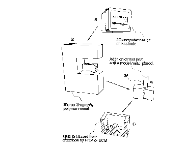
Fig. 3 illustrates the steps of the invention. Based on
a 3-D computer design a) of an electrode (or another desired
conducting element3, a polymer model b) is produced by
stereolithography (or another rapid tool-less prototyping
method). Subsequently, a tool post 36 is added and the entire
model is metal plated to form an electrode c). Through an
electro-machin;ng process such as EDM or ECM, an element of a
complicated shape ~uch as a mold d) can be produced using the
electrode c).
EXAMPLE.
A CAD design of an ECM electrode was effected using
parametric software (PR0-EN~lw~K) operating on a Silicon
Graphics computer. A commercially available stereolithography
apparatus (SLA), model SLA250 manufa~Luled by 3D Systems Inc.,
Valencia, California was used. The monomer used in the
process, a polyamide precursor, was supplied by DuPont and was
compatible with the W wavelength of the laser built into the
SLA system. Copper plating was effected using an electroless
plating process following standard practices for metallizing
of polymers. Care was taken to ensure the surface of the
polymer part was completely cured and thoroughly clean prior
to plating. The plating ~h~s~ness was .005 inches. An
allowance was made in the design to compensate for the extra
t~h; c~ ~$S -
It is important to note that the intermediate material
used in the tool-less prototyping step, can be a metal, as
explAi~e~ in the Lightman referencel above. ~owever, the
metallic replica may be made of a poor electrical conductor
such as lead or zinc and may still reguire plating with copper
or another material with a good electric co~ ctivity.
11
--' 2~0~
Generally, the most convenient materials to use in the tool-
less prototyping step are polymers which do require subsequent
coating, or partial coating, with a layer of a good electrical
conductor.
The time to build the polymer component of the electrode
will vary with size. Most electrodes within the size range of
EDM machines can be built overnight as the SLA system can run
unatt~n~e~. Large electrodes may take as much as a day of
continuous building. In the case of smaller electrodes,
several pieces can be made in a batch.
It is an advantage of the invention that flllch;ng holes,
which are a fundamental requirement of the EDM process for
complex geometries, can be built directly into the part by the
SLA. The subsequent plating process does not block the holes.
It is also an advantage of the invention that alignment
devices, ~uch as a suitable shank to fit the collet in a EDM
machine, can be added as a feature of the design. A metal
shank may be added after the polymer has cured and prior to
co~e~ plating. The shank is also plated to ensure uniform
conductivity. Metal Rh~nkR are most likely required for
electrQdes wlth large surface areas in order to carry the
higher currents, and this is also true in the case of ECM
catho~R. Heavier coppDr plates may be nec~ss~ry in the case
of large electrodes for ECM which are required to carry high
~l,enL densities, and the limitations can be calculated
readily based on Ohm's laws.