Sélection de la langue

Search

Sommaire du brevet 2109007 

Énoncé de désistement de responsabilité concernant l'information provenant de tiers

Une partie des informations de ce site Web a été fournie par des sources externes. Le gouvernement du Canada n'assume aucune responsabilité concernant la précision, l'actualité ou la fiabilité des informations fournies par les sources externes. Les utilisateurs qui désirent employer cette information devraient consulter directement la source des informations. Le contenu fourni par les sources externes n'est pas assujetti aux exigences sur les langues officielles, la protection des renseignements personnels et l'accessibilité.

Disponibilité de l'Abrégé et des Revendications

L'apparition de différences dans le texte et l'image des Revendications et de l'Abrégé dépend du moment auquel le document est publié. Les textes des Revendications et de l'Abrégé sont affichés :

  • lorsque la demande peut être examinée par le public;
  • lorsque le brevet est émis (délivrance).
(12) Brevet: (11) CA 2109007
(54) Titre français: DISPOSITIF D'ASSIGNATION DE TRANCHES DE TEMPS POUR SYSTEME DE COMMUNICATION
(54) Titre anglais: TIME SLOT ASSIGNER FOR COMMUNICATION SYSTEM
Statut: Durée expirée - au-delà du délai suivant l'octroi
Données bibliographiques
Abrégés

Abrégé français

L'invention porte sur une méthode d'assignation de données provenant d'intervalles de temps d'un bus d'entrée à des intervalles de temps d'un bus de sortie, dans laquelle on détermine l'ordre des intervalles de temps de données d'une trame d'entrée, de façon à déterminer si les données de chaque intervalle de temps d'une trame d'entrée doivent être placées dans le même intervalle de temps ou dans un intervalle ultérieur d'une trame de sortie, ou si elles doivent être placées dans un intervalle de temps antérieur de la trame de sortie. Si les données de chaque intervalle de temps de la trame d'entrée doivent être placées dans le même intervalle de temps ou dans un intervalle ultérieur d'une trame de sortie, les données de chaque intervalle de temps de la trame d'entrée sont appliquées au même intervalle de temps ou à un intervalle ultérieur de la trame de sortie. Si les données d'un intervalle de temps de la trame d'entrée doivent être placées dans un intervalle de temps antérieur d'une trame de sortie, un retard d'un intervalle de temps est appliqué et les données de chaque intervalle de temps de la trame d'entrée sont appliquées au même intervalle de temps ou à un intervalle ultérieur de la trame de sortie. Ainsi, l'ordre des intervalles de temps dans un flux de données de sortie va toujours d'un intervalle de temps antérieur à un intervalle de temps ultérieur.


Abrégé anglais


The present invention relates to a method
of assigning data from time slots on an input bus to
time slots on an output bus comprised of determining the
order of time slots of data in an input frame,
determining whether each time slot of data in an input
frame is to be located in the same or later time slot in
an output frame, or whether it is to be located in an
earlier time slot in the output frame. If each time
slot of data of the input frame is to be located in the
same or in a later time slot in an output frame,
applying each time slot of data of the input frame to
the same or a later time slot in the output frame. If a
time slot of data of the input frame is to be located in
an earlier time slot in an output frame, delaying for
one time slot interval and then applying each time slot
of data of the input frame to the same or a later time
slot in the output frame. Thus the order of time slots
in a stream of output data is always from an earlier
time slot to a later time slot.

Revendications

Note : Les revendications sont présentées dans la langue officielle dans laquelle elles ont été soumises.


I Claim:
1. A method of assigning data from time slots
on an input bus to time slots on an output bus
comprising:
(a) detecting the order of time slots of data
in an input frame,
(b) detecting whether each time slot of data
in an input frame is to be located in the same or later
time slot in an output frame, or whether it is to be
located in an earlier time slot in said output frame,
(c) if each time slot of data of the input
frame is to be located in the same or in a later time
slot in an output frame, applying each time slot of data
of the input frame to the same or a later time slot in
the output frame,
(d) if a time slot of data of the input frame
is to be located in an earlier time slot in an output
frame, delaying for one time slot interval and then
applying each time slot of data of the input frame to
the same to a later time slot in the output frame,
whereby the order of time slots in a stream of
output data is always from an earlier time slot to a
later time slot.
2. A method of assigning data from time slots
on an input bus to time slots on an output bus
comprising:
(a) connecting the time slots from the input
bus to the time slots on the output bus in order
beginning with the first time slot of each frame on the
input bus,

(b) if step (a) does not result in constant
delay of time slots within a frame of data between the
input and the output bus, connecting the time slots from
the input bus to the time slots on the output bus
shifted one time slot later in time, and
(c) repeating step (b) until there is constant
delay of time slots within a frame of data between the
input and the output bus.
3. A time slot assigner for a communication
system comprising:
(a) means for receiving serial data on an
input bus divided into frames of time slots,
(b) means for converting the data of each time
slot into parallel bytes corresponding to data channels,
(c) means for storing each byte in a cycling
frame memory at locations related to channel numbers of
said data, and
(d) means for subsequently reading selectable
ones of said locations corresponding to time slot
numbers of data on an output bus, assignment of said
data being determined by
(i) connecting the time slots from the input
bus to the time slots on the output bus in order
beginning with the first slot of each frame on the input
bus,
(ii) if step (i) does not result in constant
delay of time slots within a frame of data between the
input and the output bus, connecting the time slots from
the input bus to the time slots on the output bus
shifted one time slot later in time, and

(iii) repeating step (ii) until there is
constant delay of time slots within a frame of data
between the input and the output bus.
4. A time slot assigner for a communication
system comprising:
(a) means for receiving serial data on an
input bus divided into frames of time slots,
(b) means for coverting the data of each time
slot into parallel bytes corresponding to data channels,
(c) means for storing each byte in a cycling
frame memory at locations related to channel numbers of
said data,
(d) means for subsequently reading selectable
ones of said locations corresponding to time slot
numbers of data on an output bus, said selectable ones
of said locations being determined by
(i) detecting the order of time slots of data
in an input frame,
(ii) detecting whether each time slot of data
in an input frame is to be located in the same or later
time slot in an output frame, or whether it is to be
located in an earlier time slot in said output frame,
(iii) if each time slot of data of the input
frame is to be located in the same or in a later time
slot in an output frame, applying each time slot of data
of the input frame to the same or a later time slot in
the output frame,
(iv) if a time slot of data of the input frame
is to be located in an earlier time slot in an output
frame, delaying for one time slot interval and then
applying each time slot of data of the input frame to
the same or a later time slot in the output frame,

whereby the order of time slots in a stream of
output data is always from an earlier time slot to a
later time slot.
5. A time slot assigner as defined in
claim 3 in which the means for reading selectable ones
of said locations is comprised of a connection memory
for storing location addresses of the time slots of
received data and the time slots of output data in the
storing means.
6. A time slot assigner as defined in
claim 5 in which the relationship between the location
addresses of the time slots of the received data and the
time slots of output data is fixed.
7. A time slot assigner as defined in
claim 5 in which the relationship between the location
addresses of the time slots of the received data and the
time slots of output data is variable.
8. A time slot assigner as defined in
claim 5 including means for loading said bytes of
incoming data into said storing means during a first
half of a channel interval, and means for reading data
from said storing means during a second half of the
channel interval.
9. A time slot assigner as defined in
claim 4 in which the means for reading selectable ones
of said locations is comprised of a connection memory
for storing addresses of the time slots of received data
and the time slots of output data in the storing means.

10. A time slot assigner as defined in
claim 9 in which the relationship between the location
addresses of the time slots of the received data and the
time slots of output data is fixed.
11. A time slot assigner as defined in
claim 9 in which the relationship between the location
addresses of the time slots of the received data and the
time slots of output data is variable.
12. A time slot assigner as defined in
claim 9 including means for loading said bytes of
incoming data into said storing means during a first
half of a channel interval, and means for reading data
from said storing means during a second half of the
channel interval.

Description

Note : Les descriptions sont présentées dans la langue officielle dans laquelle elles ont été soumises.


7 ~
FIELD OF THE INV~NTTON:
This invention relates to communication
systems, and in particular to switching systems for
digital data.
BACKGROUND TO THE INVENTION:
For ISDN or other applications, a
communication switching system is required to switch
data carried in standard time slots, each corresponding
to a channel, grouped in frames. This has been
typically done in ISDN systems by concatenating standard
64 kb/s channels.
Unfortunately, in many prior art switching
systems, different channels in the same bit stream
experienced different delays during the switching
operation. This resulted in data getting out of order
and becoming corrupted. Such a system is unacceptable
for ISDN applications. Canadian application Serial No.
2,076,144 published February 17, 1993 discloses a
transmission system with a delay in frames correcting
system.
Data enters a switch in specific channels, and
is stored. It is then switched by reading the store,
and leaves the switch in different channels. Since the
different output channels are not in the same sequence
as the incoming channels, different delays result from
the assignment of time slots to the data from that of
the incoming bit stream.
One of the ways of eliminating the out of
order problem due to differing delays on different
channels has been to provide a constant delay to the
data. In the past, this involved buffering an entire
frame of data and then switching this buffered data one
or more frames later. This provided the constant delay

- 2 - ~ ~ Q ~ n
by giving maximum delay to all channels. Such a
multiple frame delay is taught in the above application.
Constant delay was a requirement for data
packet switches. In such systems, the packets of data
were extracted from the data stream and were then
switched individually through a switching mechanism.
Many inputs share a common physical interface.
A protocol is established so that each of the input and
output devices can share the bandwidth of the bus, but
each has exclusive use of the bus during its period.
Newer mechanisms allow many packets to be switched at
once, but still extract the packets before switching.
SUMMARY OF THE INVENTION:
The present invention assigns outgoing
channels to incoming channels so that all channels are
switched in order, but rather than with maximum delay as
in the prior art, the present invention provides minimum
delay. The present invention also allows the switching
of constant bit rate channels of differing bit rates.
It can provide channel assignment with a constant delay
within one frame for concatenated communication
channels, and allows the assignment of incoming and
outgoing channels to provide an unambiguous constant
delay period.
With proper alignment of delay between
incoming and outgoing data streams, it is possible to
provide constant delay switching. It is also possible
to provide constant delay switching between streams of
different data rates.
In accordance with an embodiment of the
invention, a method of assigning data from time slots on
an input bus to time slots on an output bus is comprised
of determining the order of time slots of data in an

-
- 3 - ~ ~ Q ~
input frame, determining whether each time slot of data
in an input frame is to be located in the same or later
s time slot in an output frame, or whether it is to be
located in an earlier time slot in an output frame; in
the event each time slot of data of the input frame is
to be located in the same or in a later time slot in an
output frame, applying each time slot of data of the
input frame to the same or a later time slot in the
output frame; in the event a time slot of data of the
input frame is to be located in an earlier time slot in
an output frame, delay for one time slot interval and
then apply each time slot of data of the input frame to
the same or a later time slot in the output frame;
whereby the order of time slots in a stream of output
data is always from an earlier time slot to a later time
slot.
In accordance with another embodiment, a
method of assigning data from time slots on an input bus
to time slots on an output bus is comprised of firstly
connecting the time slots from the input bus to the time
slots on the output bus in order beginning with the
first time slot of each frame on the input bus; in the
event the first connecting step does not result in
constant delay of time slots within a frame of data
between the input and the output bus, secondly
connecting the time slots from the input bus to the time
slots on the output bus shifted one time slot later in
time; and repeating the second connecting step until
there is constant delay of time slots within a frame of
data between the input and the output bus.
BRI~ INTRODUCTION TO TH~ DRAWINGS:
A better understanding of the invention will
be obtained by reference to the detailed description

-
- 3a - 2 ~ ~ ~ Q ~ 7
below, in conjunction with the following drawings, in
which:
SFigure 1 illustrates frames of input data and
frames of output data relating to particular delays,
Figure 2 is a block diagram illustrating an
embodiment of the invention, and
Figure 3 illustrates a timing diagram used to
10understand the operation of the embodiment of Figure 2.
DETAILED DESCRIPTION OF THE INVENTION:
Turning to Figure 1, a pair of sequential
frame intervals labelled frame A and frame B are

~4~ 21~900~
illustrated. The line labelled input data illustrates
four incoming time slots, carrying time slot numbers 2,
3, 4 and 1. It is desired to apply data from incoming
time slots to outgoing time slots such that the data
which is in order in the incoming time slots is in order
in the outgoing time slots. This will be referred to
below as the connection of incoming to outgoing time
slots.
The assignment of time slots in the two data
streams of input data and output data is arbitrary.
There is no requirement that the pattern of outgoing
time slots should depend on the pattern of incoming time
slots. If the data in the incoming time slots, for
example, were in order by channel ABCD, connections
would be made such that the outgoing data would be again
be in order by channel ABCD with the minimum delay.
In order to understand the description below,
the following is defined. A time slot is considered to
be numbered greater than another time slot if it occurs
later in the frame, and thus it is given a greater time
slot number. A time slot is considered numbered lesser
if it occurs earlier in the frame than another time
slot. A connection is called SF (same frame) if it
connects an incoming time slot to a greater or equal
outgoing time slot. A connection is called PF (previous
frame) if it connects an incoming time slot with a
lesser time slot. In an SF connection, the data in the
outgoing frame came from the same frame on the incoming
channels. In a PF connection, the data in the outgoing
frame came from the immediately previous frame on the
incoming channels.
A connection passes data in order if it meets
the following requirements:
(a) The connections between incoming and
outgoing time slots must be in sequence. The sequence

' -
_ 5 _ ~ 7 -4
may be allowed to wrap around the end of the frame, as
s may be seen with the numbered time slots in the input
data of Figure 1.
(b) All connections must be PF;
or
All the connections can be listed starting
from the first incoming time slot in two groups with all
SF connections to the left and all PF connections to the
right. Thus in the input data figure shown in Figure 1,
the connections can be listed with the order of the
incoming channels as SF, SF, SF, PF.
Thus the output data can be checked to
determine whether there is constant delay within a frame
of data between the input and output bus. In order to
produce the constant delay, the incoming time slots
should be connected to the outgoing time slots in order,
beginning with the first of each. This is illustrated
in Figure 1, where the output data with no delay shows
the input time slot 2 connected to output time slot 2,
input time slot 3 connected to output time slot 3, etc.
It should be determined whether each time slot of data
in the input frame is to be located in the same or later
time slot in the output frame, or whether it is to be
located in an earlier time slot in an output frame. If
each time slot of data of the input frame is to be
located in the same or later time slot in an output
frame, each time slot of data of the output frame is
applied to the same or a later time slot in the output
frame. This does not exist in the example shown in
Figure 1.
However in the event a time slot of data of
3s the input frame is to be located in an earlier time slot
of an output frame, there should be delay for one time

6 2 1~g0~7
slot interval, and each time slot of data of the input
frame should be applied to the same or later time slot
in the output frame.
The time slot numbered 1 in the input data of
Figure 1 follows a higher numbered time slot, and
therefore it meets the last-noted criterion. A delay is
introduced, and the time slot data of the frame
indicated is shifted as shown in the data line shown as
OUTPUT DATA T2. It may be seen that the time slot 1 has
been shifted into the first time slot of the following
frame, thus rendering the time slots in the second
frame, frame B, in numerical sequence. All of the time
slots in frame B will thus be designated SF.
Thus it has been determined that if the
incoming time slots connected to the outgoing time slots
in order beginning with the first of each did not
produce the desired requirements, and the incoming time
slots are connected to the outgoing time slots such that
the connections are shifted one time slot later in time
than the previous connection.
Clearly the connection has a delay of less
than one frame, and in the example shown, has a delay of
only a single time slot. The delay results in the
minimum possible delay for the set of time slots given.
In the event this shift does not result in
constant delay of time slots within a frame of data
between the input and output bus, the step is repeated
again, shifting one time slot at a time, until there is
constant delay of time slots within a frame of data
between the input and output bus.
In order to effect the above, the switching
circuitry must be able to switch without substantial
delay from an incoming time slot to an outgoing time
slot which has the same or greater time slot number, and

~_ ~7~ 21~07
the switching mechanism must be able to switch from an
incoming time slot to an outgoing time slot up to one
frame time away.
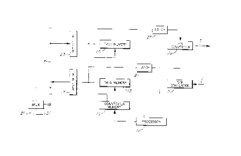
Considering Figures 2 and 3, an embodiment of
a system for effecting the above, an input serial bus 1
carries frames of serial data in 8 bit bytes, each
designating a time slot. A parallel bus 3 carries time
slot assigned data which is to be e.g. switched in a
space division switching mechanism from one bus to
another.
Similarly, data received from bus 3 is time
slot assigned and eventually output on serial output bus
5. Those buses can be wired, optical fiber, etc.
Bus 3 can interface a multiplexer connected to
e.g. 16 buses. The structure between the serial buses
and bus 3 interconnects the data carried on bus 3 with
the serial data stream. The function is to reassign
data channels so that data can be transferred between
the two buses. In one embodiment, data is created in
fixed channels by interfaces connected to the buses
multiplexed and connected to bus 3. The fixed channels
are reassigned to variable channels by the structure
described herein to allow the data to be switched
through a central space switch.
A channel consisting of e.g. 8 bits of data
arrives on the input serial databus 1 stream. In a
preferred embodiment there are 256 channels for each
125 ~s frame. The data is converted from serial to
parallel in S/P converter 7, and at the end of the
incoming channel time, it is latched to a register 9,
where it is stored for the next channel time, while the
next channel is being converted from serial to parallel.
During the first half of the next channel
time, the outputs of the register 9 are enabled under
control of processor 11. The data stored in latch 9 is

_ -8- 21~U07
received in a memory 13. Memory 13 is 256 bytes long by
8 bits wide, and thus has sufficient capacity to hold
one frame of data. Memory 13 is thus a cyclic memory
which holds the last frame of data.
s Under control of processor 11, a connection
memory 15 generates addresses and applies those
addresses to memory 13 to store the incoming data from
latch 9 at locations related to the channel number of
the incoming serial data stream.
During the second half of the channel time,
the connection memory generates addresses relating to
the time slot number of the serial channel which is to
be switched to bus 3. Upon addressing memory 13 during
the second half of the channel time and enabling memory
13 to read, rather than write the data as it had during
the first half of the channel time, the data
corresponding to the time slot number of the serial
channel which is to be switched to bus 3 is read into
buffer 17. The output buffer is enabled and the data is
output to bus 3.
Thus by appropriately designating the output
channel addresses, the data read into and stored in
memory 13 can be output to bus 3 with an appropriate
delay, and in a selectable sequence.
The data on bus 3 is then latched into
multiplexer/demultiplexer 19, for application to
appropriate serial buses 21.
The system involving transmission of data from
buses 21 to serial bus 5 is similar to that described
above, except in reverse. Demultiplexed data on bus 3
is applied to buffer 23, is written into frame memory
25, is read into latch 27 from memory 25, is converted
from latch 27 into serial data in parallel to serial
converter 29, and is output on serial data bus 5.

- 21~30~7
g
_
It will be noted that there is a difference in
speed between the bus rate on bus 1 and the bus rate on
buses 21. If data is to be switched to or from the same
numbered channels, the reading time of memory 13 should
S be established so that there is a delay between the bus
21 and bus 1.
The circuit must arrange delay between the
data on any of buses 21 and that on outgoing serial bus
5. The frame of the outgoing serial bus 5 should be
established so that it is one input bus channel time
behind the input bus 21 frame. In this way, data on
e.g. channel 0 of the input bus 21 may be switched to
channel 0 of the outgoing serial stream on bus 5.
With the above structure, it is possible to
switch data from bus 21 to bus 5 in the same manner as
previously described for data from bus 1 being switched
to serial streams on buses 21.
The timing illustrated in Figure 3 facilitates
sharing of the bandwidth of the parallel bus 3 by
alternating its use between transmit and receive data.
The internal latching of data in the transmit time slot
assignor involving elements 23, 25, 27 and 29 is similar
to the latching of data in the received time slot
assignor involving elements 7, 9, 13 and 17.
With proper delay, it is possible to switch
data between streams of different but compatible rates.
For example one can set the ratio between 1:1 and 16:1
or a higher ratio.
It should be noted that the addresses
generated by the connection memory can be completely
arbitrary. All that need occur is that each incoming
channel is stored in a known location. The locations
generated for the outgoing channels will be those known
locations.

210~
- 10-
',_
There could be for example, fixed incoming
channels and variable outgoing channels, variable
incoming channels and fixed outgoing channels, fixed
incoming channels and fixed outgoing channels or
S variable incoming channels and variable outgoing
channels. Fixed in this case designates locations fixed
relative to system timing.
Where there is variable incoming to variable
outgoing channels, it may be desired to switch only a
few channels from serial streams containing a great many
channels. In that case only those channels which are to
be switched need to be stored while the others are
ignored. This could allow the operation of a circuit
with smaller data memories 13 and 25.
A person understanding this invention may now
conceive of alternative structures and embodiments or
variations of the above. All of those which fall within
the scope of the claims appended hereto are considered
to be part of the present invention.

Dessin représentatif
Une figure unique qui représente un dessin illustrant l'invention.
États administratifs

2024-08-01 : Dans le cadre de la transition vers les Brevets de nouvelle génération (BNG), la base de données sur les brevets canadiens (BDBC) contient désormais un Historique d'événement plus détaillé, qui reproduit le Journal des événements de notre nouvelle solution interne.

Veuillez noter que les événements débutant par « Inactive : » se réfèrent à des événements qui ne sont plus utilisés dans notre nouvelle solution interne.

Pour une meilleure compréhension de l'état de la demande ou brevet qui figure sur cette page, la rubrique Mise en garde , et les descriptions de Brevet , Historique d'événement , Taxes périodiques et Historique des paiements devraient être consultées.

Historique d'événement

Description Date
Lettre envoyée 2015-06-30
Lettre envoyée 2014-03-13
Lettre envoyée 2014-03-04
Lettre envoyée 2014-02-20
Inactive : Périmé (brevet - nouvelle loi) 2013-10-22
Lettre envoyée 2013-04-29
Lettre envoyée 2013-04-11
Lettre envoyée 2013-03-28
Lettre envoyée 2010-03-31
Lettre envoyée 2009-04-29
Lettre envoyée 2007-10-19
Inactive : CIB de MCD 2006-03-11
Lettre envoyée 2005-09-09
Lettre envoyée 2003-12-01
Inactive : Correspondance - Transfert 2003-09-29
Inactive : Lettre officielle 2003-04-17
Lettre envoyée 2001-06-13
Inactive : TME en retard traitée 2000-10-06
Lettre envoyée 1999-10-22
Accordé par délivrance 1999-05-04
Préoctroi 1999-01-29
Inactive : Taxe finale reçue 1999-01-29
Un avis d'acceptation est envoyé 1998-08-31
Lettre envoyée 1998-08-31
Un avis d'acceptation est envoyé 1998-08-31
Inactive : Renseign. sur l'état - Complets dès date d'ent. journ. 1998-08-25
Inactive : Dem. traitée sur TS dès date d'ent. journal 1998-08-25
Inactive : Approuvée aux fins d'acceptation (AFA) 1998-08-12
Demande publiée (accessible au public) 1995-04-23
Exigences pour une requête d'examen - jugée conforme 1993-10-22
Toutes les exigences pour l'examen - jugée conforme 1993-10-22

Historique d'abandonnement

Il n'y a pas d'historique d'abandonnement

Taxes périodiques

Le dernier paiement a été reçu le 1998-10-08

Avis : Si le paiement en totalité n'a pas été reçu au plus tard à la date indiquée, une taxe supplémentaire peut être imposée, soit une des taxes suivantes :

  • taxe de rétablissement ;
  • taxe pour paiement en souffrance ; ou
  • taxe additionnelle pour le renversement d'une péremption réputée.

Les taxes sur les brevets sont ajustées au 1er janvier de chaque année. Les montants ci-dessus sont les montants actuels s'ils sont reçus au plus tard le 31 décembre de l'année en cours.
Veuillez vous référer à la page web des taxes sur les brevets de l'OPIC pour voir tous les montants actuels des taxes.

Historique des taxes

Type de taxes Anniversaire Échéance Date payée
TM (demande, 4e anniv.) - générale 04 1997-10-22 1997-10-02
Enregistrement d'un document 1998-02-16
TM (demande, 5e anniv.) - générale 05 1998-10-22 1998-10-08
Taxe finale - générale 1999-01-29
Annulation de la péremption réputée 1999-10-22 2000-09-19
TM (brevet, 6e anniv.) - générale 1999-10-22 2000-09-19
TM (brevet, 7e anniv.) - générale 2000-10-23 2000-10-06
Enregistrement d'un document 2001-05-04
TM (brevet, 8e anniv.) - générale 2001-10-22 2001-09-18
TM (brevet, 9e anniv.) - générale 2002-10-22 2002-09-19
Enregistrement d'un document 2003-03-24
TM (brevet, 10e anniv.) - générale 2003-10-22 2003-09-17
TM (brevet, 11e anniv.) - générale 2004-10-22 2004-09-09
Enregistrement d'un document 2005-07-18
TM (brevet, 12e anniv.) - générale 2005-10-24 2005-09-08
TM (brevet, 13e anniv.) - générale 2006-10-23 2006-09-08
TM (brevet, 14e anniv.) - générale 2007-10-22 2007-09-07
Enregistrement d'un document 2007-09-14
TM (brevet, 15e anniv.) - générale 2008-10-22 2008-09-15
Enregistrement d'un document 2009-02-24
TM (brevet, 16e anniv.) - générale 2009-10-22 2009-09-14
Enregistrement d'un document 2010-01-14
TM (brevet, 17e anniv.) - générale 2010-10-22 2010-09-16
TM (brevet, 18e anniv.) - générale 2011-10-24 2011-09-20
TM (brevet, 19e anniv.) - générale 2012-10-22 2012-09-12
Enregistrement d'un document 2013-03-12
Enregistrement d'un document 2013-03-28
Enregistrement d'un document 2014-02-04
Enregistrement d'un document 2014-02-13
Enregistrement d'un document 2015-05-04
Titulaires au dossier

Les titulaires actuels et antérieures au dossier sont affichés en ordre alphabétique.

Titulaires actuels au dossier
MITEL NETWORKS CORPORATION
Titulaires antérieures au dossier
THOMAS GRAY
Les propriétaires antérieurs qui ne figurent pas dans la liste des « Propriétaires au dossier » apparaîtront dans d'autres documents au dossier.
Documents

Pour visionner les fichiers sélectionnés, entrer le code reCAPTCHA :


Pour visualiser une image, cliquer sur un lien dans la colonne description du document. Pour télécharger l'image (les images), cliquer l'une ou plusieurs cases à cocher dans la première colonne et ensuite cliquer sur le bouton "Télécharger sélection en format PDF (archive Zip)" ou le bouton "Télécharger sélection (en un fichier PDF fusionné)".

Liste des documents de brevet publiés et non publiés sur la BDBC .

Si vous avez des difficultés à accéder au contenu, veuillez communiquer avec le Centre de services à la clientèle au 1-866-997-1936, ou envoyer un courriel au Centre de service à la clientèle de l'OPIC.


Description du
Document 
Date
(aaaa-mm-jj) 
Nombre de pages   Taille de l'image (Ko) 
Abrégé 1995-06-05 1 45
Revendications 1995-06-05 4 257
Dessins 1995-06-05 2 67
Description 1995-06-05 10 616
Description 1998-07-21 11 435
Abrégé 1998-07-21 1 27
Revendications 1998-07-21 5 160
Dessins 1998-07-21 2 32
Dessin représentatif 1999-04-26 1 7
Dessin représentatif 1998-07-28 1 12
Avis du commissaire - Demande jugée acceptable 1998-08-30 1 166
Avis concernant la taxe de maintien 1999-11-21 1 178
Avis concernant la taxe de maintien 1999-11-21 1 179
Quittance d'un paiement en retard 2000-10-11 1 171
Correspondance 2003-04-16 1 17
Correspondance 1999-01-28 2 65
Taxes 1998-10-07 1 43
Taxes 2000-10-05 3 118
Taxes 1997-10-01 1 33
Taxes 1996-10-03 1 34
Taxes 1995-10-02 1 28
Correspondance de la poursuite 1994-06-06 3 164
Demande de l'examinateur 1997-12-04 1 28
Correspondance de la poursuite 1998-05-12 3 132