Note : Les descriptions sont présentées dans la langue officielle dans laquelle elles ont été soumises.
2~-~0472 ZJ
EN9-93-001
METHOD AND APPARATUS FOR
IN-SITU TESTING OF INTEGRATED CIRCUIT CHIPS
FIELD OF THE INVENTION
The invention relates to integrated circuit chip testing.
Typically, integrated circuit chips are attached to a chip carrier,
thermally conductive module chip carrier, circuit card or board,
e.g., by solder bonding, controlled collapse chip connect, or the
like. For the first time since the wafer was diced, the chip is
tested, e.g., electrically tested and logically tested. Some of
the tests are subtle, for example tests for active and passive
pattern faults and "stuck at 1" or "stuck at 0~ faults. When a
fault is found, the chip is removed from the card or board. This
is not a simple "desoldering~ step, especially in the case of high
input/output (I/O) density integrated circuit chips, bonded with
encapsulation chip connect technologies, and usually present in
multi-chip modules. When a chip is found to be defective, it must
be removed, the chip site redressed, and a new chip installed for
testing. In the case of a polymeric substrate, redressing the chip
site might include milling.
According to the method of the invention, there is provided a
method of testing semi-conductor chips. The individual
semiconductor chips have I/O, power, and ground contacts. In the
method of the invention a chip carrier is provided. The chip
carrier may be the substrate, or a dedicated fixture just for
testing chips. This chip carrier has contacts corresponding to the
contacts on the semiconductor chip. The carrier contacts are low
contact resistance contacts adapted for holding the integrated
circuit chip in place during testing, with low impedance, while
allowing easy removal of defective chips and their replacement by
other chips.
According to the invention the test fixture contacts have
dendritic surfaces. By dendrites are meant essentially vertical
members extending outwardly from a generally planar area of
conductive material. The dendrites, produced by a columnar growth
process, generally have an aspect ratio, of vertical to horizontal
dimensions, of at least about 1.0, a height above the planar area
2110472
EN9-93-001 2
of conductive material of about 10 to 100 micrometers.
The chip contacts are brought into conductive contact with the
dendrite bearing conductor pads on the chip carrier. Conductive
contact requires a low impedance, low contact resistance contact,
with the integrated circuit chips being secured from lateral
movement with respect to the substrate or fixture. Test signal
input vectors are applied to the inputs of the semiconductor chip,
and output signal vectors are recovered from the semiconductor
chip.
In the case where the substrate is a temporary test fixture,
the chips may be removed from the fixture and either discarded or
attached to a suitable substrate. Alternatively, when the chips
have been tested in situ, the tested and qualified chips may be
bonded through the dendritic conductor pads to the substrate, and
the chips which have failed may be removed and discarded without
causing need for repair or redressing of the chip site prior to
placement of another chip.
BACKGROUND OF THE INVENTION
In the population of integrated circuit chip carriers,
including thermally conductive modules, ceramic substrates, and
polymeric substrates, it is necessary to minimize the shipment of
modules with defective integrated circuit chips, while minimizing
the cost of testing and replacement.
Integrated circuit are subjected to various wafer level tests
during various stages of fabrication prior to dicing. However,
after dicing it is particularly difficult and expensive to test
integrated circuit chips. One reason is that an integrated circuit
chip must be tested through its I/O and pads before populating of
the carrier, card, board, or the like.
In populating a card, board or other packages integrated
circuit chips are attached to a circuit card or board, e.g., by
solder bonding, controlled collapse chip connect, wire lead
bonding, or the like. The chip is then tested as part of an
assembly, e.g., electrically tested and logically tested. Some of
the tests are subtle, for example tests for active and passive
2110~72
EN9-93-001 3
pattern faults and "stuck at 1" or "stuck at 0" faults. When a
fault is found, the chip is removed from the card or board. This
is not a simple "desoldering" step, especially in the case of high
I/O density chips, encapsulation chip connect technologies, and
multi-chip modules, where the chip must be removed, the chip site
redressed, and a new chip installed for testing. In the case of a
polymeric substrate, redressing the chip site might include
milling.
Dendritic Chip Testers
"High Performance Test System", IBM Technical Disclosure
Bulletin, Volume 33, No. lA (June 1990), pp 124-125 describes a
test system for ULSI integrated circuit memory and logic chips. In
the described method, a first silicon wafer "test board" has
metallization complementary to the metallization of the second
silicon wafer to be tested. The second silicon wafer has C4
(controlled collapse chip connection) PbSn solder balls on the
contacts. The first and second silicon wafers have substantially
flat and substantially parallel surfaces, and are said to require
a minimum of compressive force for testing.
Anonymous, "New Products Test Interposer" Research Disclosure,
January 1990, Number 309 (Kenneth Mason Publications Ltd., England)
describes a method for fabricating an interposer-type test head to
perform electrical testing of printed circuit cards and boards
prior to component assembly. The test interposer is built as a
mirror image circuit of the circuit to be tested. However, only
the points to be tested, as lands and pads, are present. Circuit
lines are not present. The test interposer pads are coated with a
dendritic material to make electrical contact to the corresponding
points on the printed circuit component to be tested. The circuit
board or card and the tester are then brought into contact for
testing.
Testers
Compressive type testers are described generally in U.S.
Patent 4,716,124 to Yerman et al. for TAPE AUTOMATED MANUFACTURE OF
POWER SEMICONDUCTOR DEVICES, U.S. Patent 4,820,976 to Brown for
TEST FIXTURE CAPABLE OF ELECTRICALLY TESTING AN INTEGRATED CIRCUIT
21104~2
EN9-93-001 4
DIE HAVING A PLANAR ARRAY OF CONTACTS, and U.S. Patent 4,189,825 to
Robillard et al. for INTEGRATED TEST AND ASSEMBLY DEVICE.
U.S. Patent 4,189,825 to Robillard et al. for INTEGRATED TEST
AND ASSEMBLY DEVICE describes a chip of the beam lead type with
sharp points on the substrate leads and etched, conical holes in
the semiconductor. The semiconductor and conical holes are
metallized with a thin, conformal metal film, leaving conical
openings in the metallization. These apertures correspond to the
sharp points on the substrate leads. According to Robillard et al,
the chips may be assembled and tested, with faulty chips removed
and replaced before bonding. Bonding is by ultrasonic welding.
Dendritic Connections
Dendritic connections are described in commonly assigned
United States Patent 5,137,461 of Bindra et al for SEPARABLE
ELECTRICAL CONNECTION TECHNOLOGY. Bindra et al describe separable
and reconnectable electrical connections for electrical equipment.
Bindra et al's connectors have dendrites characterized by an
elongated, cylindrical morphology. These cylindrical dendrites are
prepared by a high frequency, high voltage, high current density,
pulse plating methodology utilizing a low metal ion concentration
electrolyte. Bindra et al describe the pulsed electrodeposition of
Pd from a 10-150 millimolar Pd tetramine chloride, 5 molar ammonium
chloride solution at 50 to 450 hertz and 200 to 1100 milliamperes
per square centimeter in a pulse plating technique.
Electrodeposition of Pd dendrites is further described in
European Patent 0054695 and U.S. Patent 4,328,286 (European Patent
0020020)
U.S. Patent 4,328,286 (European Patent 20020) to Crosby for
ELECTROPLATING A SUBSTRATE WITH TWO LAYERS OF PALLADIUM describes
producing a low porosity Pd coating for electrical contacts. The Pd
coating is prepared by electrodepositing a first layer of Pd from
an aqueous bath containing the cationic complex Pd (NH3)4++ and free
ammonia with supporting anions (Cl-, Br~, NH2S03-, N02- and N03-) and
then electrodepositing a second Pd layer from an aqueous bath
containing the anionic complex Pd(N02)24- with supporting cations.
-
EN9-93-001 5 ~ 4 7 ~
Commonly assigned European Patent 54695 (published June 30,
1982, granted September 11, 1985 discloses a method of preparing a
Pd electrical contact by electrodeposition from a relatively dilute
solution that is sprayed onto a cathode which is located
completely outside and above the surface of the solution, which is
located in a tank. The solution forms a continuous curtain falling
from the bottom end of the cathode back into the tank. A higher
electric current than usual is used in the deposition process. The
dendrites obtained have a larger cross-section than those obtained
in conventional processes.
SummarY
The art has failed to provide a means for actual or simulated
in situ testing of integrated circuit chips, especially "flip
chips", allowing bonding if the chips are satisfactory and
replacement if the chips are unsatisfactory.
OBJECTS OF THE INVENTION
It is an object of the invention to provide for simulated and
actual in situ testing of integrated circuit chips.
It is a further object of the invention to provide a method
and apparatus for in situ testing of integrated circuit chips that
allows for easy permanent chip attachment of satisfactory chips and
easy removal of unsatisfactory chips.
SUMMARY OF THE INVENTION
According to the method of the invention, there is provided a
method of testing semiconductor chips. The integrated circuit chips
are tested under either simulated or actual in situ conditions. In
a preferred exemplification the method and apparatus of the
invention allows for easy permanent chip attachment of satisfactory
chips and easy removal of unsatisfactory chips.
In the method of the invention a chip carrier is provided.
The chip carrier may be the substrate or a fixture just for testing
chips. This chip carrier has contacts corresponding to the contacts
on the semiconductor chip. The carrier contacts have dendritic
EN9-93-001 6 2 i 10 ~ ~ 2
surfaces.
The chip contacts are brought into conductive contact with the
conductor pads on the chip carrier. Test signal input vectors are
applied to the inputs of the semiconductor chip and output signal
vectors are recovered from the semiconductor chip.
After testing the chip may be removed from the substrate.
Alternatively, the chip may be bonded through the dendritic
conductor pads to the substrate after successful testing.
As used herein, "dendrites" are high surface area conductive
pads and contacts formed of essentially vertical members extending
outwardly from a generally planar area of conductive material. The
dendrites, produced by a columnar growth process, generally have an
aspect ratio of vertical to horizontal dimensions of at least about
1.0 and a height above the planar area of conductive material of
about 10 to 100 micrometers.
The dendritic morphology is obtained by electroplating the
underlayer under conditions that give rise to columnar growth; that
is, very low metal cation concentration in the electrolyte, with
electroplating being carried out at a high voltage, high current,
and a high current density. Preferably, the electroplating current
is a pulsed current.
The resulting dendrites have a peak height of about 10 to 100
microns and a density (dendrites per unit area) of about 200 to 500
dendrites per square millimeter.
Dendrites have a chip connect pad to dendritic pad contact
resistance of about 3 to 5 milliohms.
BRIEF DESCRIPTION OF THE FIGURES
The invention may be understood by reference to the FIGURES.
FIGURE 1 is a representation of dendritic connectors, shown in
cutaway view.
FIGURE 2 is a schematic flow chart of the method of the
EN9-93-001 7 2110472
invention.
~ IGURE 3 is a circuit diagram of a RAM and decoder used to
illustrate test vectors.
FIGURE 4 is a representation of passive faults in a Random
Access Memory (RAM) cell.
FIGURE 5 is a representation of active faults in a Random
Access Memory (RAM) cell.
FIGURES 6A and 6B show the voltage versus time plots for
pulsed electroplating. FIGURE 6A is a representation of the
voltage versus time for the t'on/off" electroplating method of the
prior art. FIGURE 6B is a representation of the voltage versus time
plot for the reversal method of a preferred embodiment of the
invention herein.
~ETAILED DESCRIPTION OF THE INVENTION
According to the method of the invention, there is provided a
method of testing and, in a preferred embodiment of the invention,
installing, semi-conductor chips. The individual semiconductor
chips have I/O, power, and ground contacts. In the method of the
invention a chip carrier is provided. The chip carrier may be the
substrate or a fixture just for testing chips. This chip carrier
has contacts corresponding to the contacts on the semiconductor
chip. The carrier contacts have conductive surfaces with provision
for enhanced electrical contact, such as columnar dendritic
surfaces or polymer core conical connector surfaces, to yield
certain and reliable electrical contact over the entire array of
carrier contacts.
The chip contacts are brought into conductive contact with the
conductor pads on the chip carrier. Test signal input vectors are
applied to the inputs of the semiconductor chip and output signal
vectors are recovered from the semiconductor chip.
After testing the chip may be removed from the substrate.
Alternatively, the chip may be bonded through the dendritic
conductor pads to the substrate after successful testing.
2110472
EN9-93-001 8
Dendrites
Dendrites are high surface area connectors. They can be used
as "pad on pad" connectors, and for chip burn in. Dendrites have
the structure shown in FIGURE l, with (a) a conductive pad or
substrate, such as a Cu pad, (b) a "smooth" underlayer, as a smooth
Pd underlayer, and (c) an overlayer, as a columnar Pd layer. The
substrate underlying the conductive pad can be a printed circuit
board, a metallized ceramic, or a metal pad on a flexible circuit.
The underlayer can be a Pd thin film, e.g., a Pd layer direct
current plated from a relatively concentrated electroplated bath.
The outer layer is a columnar Pd layer, typically deposited from
an electroplating solution that is dilute in metal cation
concentration, with a pulsed, high voltage, high current, high
current density electroplating solution. There may, optionally, be
a gold layer, or a solder layer, as a Bi-Sn or Pb-Sn layer, atop
the Pd layer for bonding.
The dendritic morphology iB obtained by electroplating the
underlayer under conditions that give rise to columnar growth, that
is, very low metal cation concentration in the electrolyte, with
electroplating being carried out at a high voltage, a high current,
and a high current density. Preferably the electroplating current
is a pulsed current. In the case of a particularly preferred
embodiment of the invention the plating current is pulsed positive
and negative.
The dendritic surface is prepared by first electroplating a
smooth Pd coating, referred to in the electroplating as a shiny or
reflective plate, onto Cu pads. This smooth Pd layer is deposited
from a relatively concentrated Pd electroplating solution,
containing about 100 or more millimoles of Pd or more, at a low
current density of about 5 to 20 milliamperes per square centimeter
or lower.
A columnar Pd layer is applied atop the Pd undercoat. This
columnar, coat is applied from a relatively dilute Pd
electroplating solution having a Pd concentration of about 10-50
millimoles per liter in Pd (versus about 100 millimoles of Pd per
liter for conventional electroplating). Typical electroplating
solutions include palladium tetra-amine chloride/ ammonium
2110472
EN9-93-001 9
chloride, at a pH of about 9 to 10. Typical pulsed electroplating
programs include a ten to twenty percent duty cycle, and a current
density of about 500 to 1000 mA/cm2.
While satisfactory results are obtained with a single phase
pulsed current, as shown in FIGURE 6A, and denominated "Prior Art,"
we have found that superior results are obtained with about 2.5
percent to about 25% voltage reversal with a two phase
electroplating cycle, as shown in FIGURE 6B. By "single phase"
pulsed electroplating cycle, we mean an electroplating current that
is pulsed to zero and positive values. By a "two phase" pulsed
electroplating cycle we mean an electroplating current that is
pulsed to zero and positive values and to zero and negative values,
as shown in FIGURE 6B.
One such pulse pattern that we have found particularly
outstanding has the following characteristics:
POSITIVE PULSE CONDITIONS
Peak Current Density 200-400 Amperes/ft2
Pulse Time On 0.5 to 1.0 millisecond
Pulse Time Off 2.0 to 9.0 milliseconds
Duty Cycle 10% to 20%
Positive Direction Time 20 to 40 seconds
REVERSE PULSE CONDITIONS
Peak Current Density 300 to 800 Amperes/ft2
Pulse Time On 0.5 to 1.0 millisecond
Pulse Time Off 2.0 to 9.0 milliseconds
Duty Cycle 10% to 20%
Reverse Direction Time 1 to 5 seconds
Gold, solder (as Pb-Sn or Bi-Sn) or even a thin overcoat of Pd
may be applied atop the dendrites formed thereby.
The resulting dendrites have a peak height of about 10 to 100
microns and a density (dendrites per unit area) of about 200 to
21104~2
EN9-93-001 10
500 dendrites per square millimeter. Dendrites have a chip connect
pad to dendritic pad contact resistance of about 3 to 5 milliohms.
While the invention has been described with respect to
dendrites, it is, of course, to be understood that conical
connectors may also be utilized on the substrate or fixture.
Conical connectors are described in the commonly assigned U.S.
Patent 5,118,299 of Francis C. Burns, John J. Kaufman, David E.
King, and Alan D. Knight, for CONE ELECTRICAL CONTACT, the
disclosure of which is hereby incorporated herein by reference.
Conical connectors are prepared by depositing an imagable polymeric
material, as polyimide, and forming polymeric cones, as by laser
ablation. The conical connectors are then coated, e.g., with a
sputter chromium adhesion layer approximately 150 Angstroms thick,
followed by sputter coating of a Cu layer approximately 10,000 to
100,000 Angstroms thick. A nickel coating approximately 0.1 to 1
mil thick is deposited atop the Cu, followed by a thin Au film.
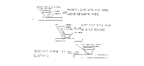
Integrated Circuit Chip Test Procedures (Test Fixture)
The integrated circuit chip is tested substantially as shown
in Figure 2. The integrated circuit chip, with connectors on its
substrate facing is positioned on the substrate or test fixture.
In a preferred embodiment the chip contacts or connectors on the
chip bonding surface have deposited solder connectors, as solder
balls or C4 (controlled collapse chip connectors) thereon for
bonding to the substrate.
The substrate or fixture has dendrites on the chip connect
surfaces, contacts, or pads, substantially as described above. The
chip and substrate are brought into contact and a compressive force
is applied to the chip and substrate. The compressive force is
sufficient to allow the dendrites to break through any oxide or
corrosion films on the solder balls or C4 connectors on the chip.
This provides direct, metal to metal contact, characterized by a
contact resistance of less then 10 milliohms, and preferably less
than 6 milliohms.
The integrated circuit chip is powered, e.g., between inputs
_ _ _
211~7~
EN9-93-001 11
of VDD or Vcc, and Ground, and subjected to various logic and memory
tests. Chips that fail to pass these tests are discarded, while
chips that pass these tests are installed in systems. In a
particularly preferred exemplification of the invention the testing
fixture is also the substrate, and chips that pass are bonded to
the substrate between the bonding pad and the dendritic surface.
Bonding may be by thermal compression bonding, transient liquid
phase bonding, solder reflow, controlled collapse chip connect (C4
bonding) or the like. In the case of polymeric substrates bonding
should take place below about 200 degrees Centigrade. After bonding
the bond, or the bond, chip, and adjacent areas of substrate, may
be encapsulated in a suitable organic encapsulant. Thus, after
testing the Au, Bi-Sn, Pb-Sn, or other low melting film, coating
or layer on the dendrites may be caused to fuse, bond, or alloy
with the older balls or low melting materials on the integrated
circuit chip to form an electrical or electrical and metallurgical
bond.
Integrated Circuit Test Procedures (Test Vectors~.
The integrated circuit chip may be tested for various defects
while in dendritic contact with the dendritic surfaced pad. While
the description herein is of the type of test procedures normally
utilized for memory chips, especially CMOS memory chips, it is, of
course, to be understood that the method of this invention is
equally applicable to logic integrated circuit chips, and even to
analog integrated circuit chips, as power processing chips and
amplifier chips.
In the case of memory chips, the chip or chips may be tested
for "cell stuck" faults. In a "cell stuck at" fault, one or more
cells or gates are stuck-at-1 or stuck-at-O. When a cell or gate
is stuck-at-x, it will remain stuck-at-x regardless of what is done
to the cell or to surrounding cells or gates.
Memory chips have a decoder. The decoder is the combinational
circuit that selects a unique memory word corresponding to an
address. Failures in decoder logic result in "no access faults"
and in "multiple access faults." In "no access faults" the decoder
will not address the accessed cell. The decoder may address non-
. _ _ _
2110~2
EN9-93-001 12
addressed cells. In "multiple access faults" the decoder will
address multiple cells, possibly including the addressed cell. *
"No access" faults are similar to "stuck-at-x" faults except
that the failure is in the decoder and not the memory array, and"
multiple access" faults are similar to "coupling" or "pattern
sensitive" faults, except, again, the failure is in the decoder and
not the memory array.
Integrated circuits are also susceptible to pattern sensitive
faults. Pattern sensitive faults exist when cells are "coupled."
Cells are "coupled" when a transition at a cell, due to a write
operation at this cell, changes the contents of a second cell,
independently of the contents of the second cell or of any other
cells. Coupling can be uni-directional, i.e., a change the state of
cell i can change the state of cell j, but a change of the state of
cell j does not change the state of cell i, or bi-directional,
i.e., a change of the state of cell i changes the state of cell j,
and a change of the state of cell j changes the state of cell i.
Typically, pattern sensitive faults are identified with capacitive
coupling and leakage currents.
Another class of faults to which integrated circuit chips,
especially memory chips, are susceptible to are faults in access
circuitry. Accessing faults occur when more then one memory cell is
accessed during a READ or WRITE operation. During a READ operation
at some address, i,j, more then one cell can be accessed, and the
output is some combinatorial function of the contents of both
cells. During a write operation at one of the "coupled" addresses,
all of the activated or accessed cells are written to
simultaneously. Other types of accessing faults occur when the
sense amplifier logic or the write driver logic are "stuck at X."
These faults may be due to capacitive coupling or due to shorts.
A memory array, with column and row decoders is shown in
Figure 3. Consider a simplified RAM having a 8X4 memory array of
8 rows by 4 words per row. The routine shown below, which requires
4n tests (where n is the number of memory cells in the memory
array) detects decoder faults and cell "stuck at" faults.
.. ....
21104'~2
EN9-93-001 13
For i = O to i = n-1
Write (ci, O)
For i = O to i = n-1
Read (ci, =O)
Write (ci, =l)
Read (ci, =1)
Another test used in testing CMOS integrated memory circuits
is the March Test. The March Test is a finite sequence of March
Elements. A March Element is a finite sequence of operations (Read,
Write 1. Write O, Write the complement) applied to every cell in
the memory array. The operations can be applied in either
increasing address order (from address O) or in decreasing address
order (from address n-1). The same operations are applied to each
cell.
There are various procedures for generating the March test
pattern. Specifically, one such procedure starts by classifying
possible physical defects (shorts, opens, oxide too thin, etc.)
likely to effect memory functionality or having a high probability
of occurrence.
Next, the circuit is simulated by a circuit simulator, as
SPICE or ASTAP. The purpose of this simulation is to determine the
impact the effect of the physical defect on the memory. Defects
can affect either memory functionality or memory performance.
The faults determined by SPICE or ASTAP simulation are then
mapped into specific memory failure modes, that is, "Stuck-At-X" or
"Access" or ""Coupling" failure modes.
Functional test patterns are then derived from the failure
modes. The test patterns are derived to cover all of the failure
modes identified for the memory.
The test patterns are then run against the simulator to insure
that the test pattern detects defined failure modes.
Most defects are memory cell defects that initially appear as
a "Stuck-At-X" defect. However, sometimes a defective cell can
2110472
EN9-93-001 14
drive the entire output of an entire row, or appear as a pattern
sensitive fault.
The March Test is particularly preferred for testing the
decoder. The March Test tests for cell "stuck at" faults, and it
tests for coupling faults. However, the March Test does not test
for pattern sensitive faults. This is because the March test is
linearly sequential, and can mask pattern sensitive faults.
In the March Test, the signal pattern is
For i = O,l,...,n-1
Write (ci, O)
For i = O,l,..,n-1
Read (ci, =O)
Write (ci, =l)
Read (c;, =1)
For i = n-1, n-2,..,0
Read (ci, =1)
Write (ci, =O)
Read (ci, =O)
Repeat the above steps, interchanging O's and l's.
The March Test detects the following faults:
a. Stuck Cell. To detect a "Stuck-At-1" fault in a memory
cell, the cell must be initialized to O, and the value O
must actually be read. If O is read, there is no "Stuck-
At-1" fault. Similarly, to detect a "Stuck-At-O" fault
in a memory cell, the cell must be initialized to 1, and
the value 1 must actually be read. If 1 is read, there is
no "Stuck-At-O" fault.
b. No-select on Write. The No select on write fault is a
Write Decoder fault. Define foflf2f3f4f5f6f7 be the memory
word not selected as the result of the fault. A
necessary and sufficient condition for detecting the No
Select On Write fault is that:
2110472
EN9-93~001 15
i. Write pattern a at word f.
ii. Write and read the complement of pattern a from f.
Since the word f can not be selected for a Write
operation, the word contains a random pattern. Writing
and reading a specific pattern is necessary to detect
this failure mode.
c. No Select On Read. This is read decoder failure mode.
d. Write Multiple Words. Let i be the word being addressed
and f be the word actually being written as a result of
the Write Multiple Words failure. To detect the Write
Multiple Words failure,
i. f should contain the complement of the pattern
written at i. This is necessary to distinguish
between the patterns at i and f.
ii. The test sequence for each word i should include
a. Read pattern a at location i.
b. Write complement of a at location i. This
reads the complement data at f before the
value in f is destroyed.
c. Ripple the linear addressing through the
memory.
If f>i and conditions i and ii are satisfied, then
the fault is detected when addressing in ascending
order. If f<i then the fault is detected when
addressing is descending order.
e. Read Multiple Words. This failure, also called multi-
select, occurs when two words are read simultaneously.
In the test for this failure mode the two words i and f
should have complementary data. The sense amplifier
should be able to discriminate between reading a
simultaneous O and 1 on the same line, and reading normal
- 21104~2
EN9-93-001 16
O's and l's.
f. Shorts Between Read Ports. This is an electrical
failure, that can result in a Read To Write Port short,
a Write to Read Port Short, or a Write To Write Port
Short.
An improved March Test Pattern that can be utilized with the
~tructure and method of the invention is:
1. Initialization to write the background pattern,
For i=1 to n-1 Write to the ith row a background
pattern~ ai-
2. Forward ripple. This reads the background pattern
and writes the complement, rippling though the
address space from O to n.
For i=l to n-1, read the background pattern, write
the complement of the background back into the row,
read the row, and increment the row decoder..
3. Reverse ripple. This reads the new background
pattern (the complement of the previous contents of
the row - hopefully), writes the complement (which
is, hopefully, the original background pattern of
the row), and ripples through the address space
from n-1 to o.
For i=n-l to 0, read the contents of the row, write
the complement of the row back into the row, and
ripple through the address space from n-l to 0.
2110~72
EN9-93-001 17
The method and structure of the invention can be used to test
for Pattern Sensitive Faults. Pattern sensitive faults can be
passive or active.
Passive pattern sensitive faults are faults such that a
pattern of cell values prevents writing a value into a cell. A
passive pattern sensitive fault pattern is shown in Figure 4. In
the Figure the states of cells, A, B, C, and D determine the state
of cell E, that is
A=B=C=D=O => E=O.
Active pattern sensitive faults occur when the change of value
in one memory cell causes the value stored in another cell to
change. An active pattern sensitive fault is shown in the Figure 5,
where the contents of cell D determine the contents of cell E. That
iS,
A=B=C ~> D,E, but
D~ => E~.
Passive pattern sensitive faults are tested for by setting the
contents of the adjacent memory cells, A,B,C,D from {0,1}, and
setting the base cell, E, to E=~ and E=~, and reading the base
cell, E. For a passive pattern sensitive fault, we expect the
measured value of the contents of cell E to be a function of the
contents of the surrounding cells, and not necessarily the value
set by the testing program.
In testing for active pattern sensitive faults, we place fixed
values in three of the four neighboring cells (i.e., three of the
four cells, A,B,C, and D), and the base cell. We then transition
the remaining neighbor cell, and see if this changes the contents
of the base cell, E.
Testing for passive pattern sensitive faults requires ~ 65_
tests, where _ is the number of cells. Testing for active pattern
sensitive faults requires ~ lOOn tests, where _ is the number of
cells.
The above described tests and test procedures may be applied
2110472
EN9-93-001 18
to an integrated circuit chip in situ in the environment where it
i8 to function in service, along with actual fan-out and latency
effects. This is a particular advantage over existing test
procedures.
While the invention has been described with respect to certain
preferred embodiments and exemplifications hereof, it is not
intended to limit the scope of the invention thereby, but solely by
the claims appended hereto.