Note : Les descriptions sont présentées dans la langue officielle dans laquelle elles ont été soumises.
2110881
ADAPTIVE EQUALIZER CAPABLE OF COMPENSATING FOR
CARRIER FREQUENCY OFFSET
BACKGROUND OF THE INVENTION
Field of the Invention:
The present invention relates to an adaptive
equalizer for use in digital cellular receiver terminals or
the like, and more particularly to an adaptive equalizer
capable of compensating for a deterioration in the channel
characteristics which results from a carrier frequency
offset.
Description of the Related Art:
Heretofore, land mobile communications systems,
typically automobile telephone system, have been analog com-
munications systems. To meet demands for a rapid increase
in the number of subscribers to such land mobile
communications systems, more diverse types of data to be
transmitted, and compatibility with ISDN (Integrated-
Services Digital Network), efforts are being made to develop
digital mobile communications systems.
For example, the Telecommunication Industries
Association in the U.S.A. established in 1989 the digital
automobile telephone standards which are summarized as
follows:
Frequency band: 800/900 MHz
Access method: TDMA
Audio encoding method: 13 kbps VSELP
2110881
Number of channels per wave: 3
Carrier interval: 60 kHz (30 kHz
interleave)
Modulation method: ~/4-shift DQPSK
Base station radius: 0.5 ~ 20 km
A ~/4-shift DQPSK (~/4-shift differentially
encoded quadrature phase shift keying) signal is a signal
which is produced by differentially encoding symbols to be
transmitted and then subjecting them to ~/4-shift QPSK.
The process of ~/4-shift QPSK Will be described
below. The differentially encoding process that has no
effect on an understanding of the present invention will not
be described below.
In ~/4-shift QPSK, a series of bits of digital
signals 0 and 1 is divided into pairs of bits, and the phase
angle ~k Of a high-frequency sine wave is determined
depending on one of 2-bit combinations 00, 01, 10, 11 (a 2-
bit combination {Xk, Yk} is referred to as a "symbol"). A
sine wave S(t) having a phase angle ~k corresponding to the
kth symbol is expressed by:
S(t) = cos(~ct + ~k) k = 1, 2, 3, 4
(-T/2 < t ' T/2) (1)
where
~k = + ~/4, + 3~/4 (2),
~ )c is the angular frequency of a carrier sine wave
(if a carrier frequency is fc~ then ~)c = 2~fc), and
T is the duration of one symbol.
2110881
The sine wave S(t) may also be expressed as fol-
lows:
S(t) = akcos(~ct) + bksin(~ct) (3)
where (ak, bk) = (1/~2,1/~2), (-1/~2,1/~2),
(-1/~2,-1/~2), (1/~2,-1/~2) (4)
a2 + b2 = 1 . (5).
The values of (ak, bk) represent the components of a symbol
on an I-Q rectangular Cartesian coordinate plane composed of
an in-phase axis (I axis) and a quadrature axis (Q axis).
FIG. 8 of the accompanying drawings shows, by way
of example, a conventional digital cellular receiver for re-
ceiving QPSK-modulated waves. It is assumed that the
digital cellular receiver has received a signal R(t) that is
expressed by:
R(t) = a'cos(~ct) + b'sin(~ct) (6)
where (a', b') is (ak, bk) that has been received (the
suffix k is omitted).
In the digital cellular receiver shown in FIG. 8,
the received signal R(t) expressed by the equation (6) is
subjected to quadrature detection to reproduce the combina-
tions (ak, bk) (and further to determine phase differences
between succeeding combinations (ak, bk) in differential
decoding) thereby reproducing the symbols, and then
demodulate the symbols into a series of bits O and 1 which
.
lS Orlglnal Serlal SlgnalS.
The quadrature detector divides the received
signal expressed by the equation (6) into two signals,
-- 3
2110881
multiplies one of the signal by a sine wave cos(oct) which
is of the same frequency and phase as the transmitted
carrier, and multiplies the other signal by a sine wave
sin(o~ct). This quadrature detection process is called a
synchronous detection process. The results of the process
are given as follows:
R(t)cos(o)ct)
= (1/2)(a' + a'cos2(1)ct + b'sin20)ct) (7), and
R(t)sin(o)ct)
= (1/2)(b' - b'cos20)ct + a'sin20)ct) (8).
The signals expressed by the above equations (7) and (8) are
passed through a low-pass filter to remove multiple
frequency components therefrom, thus obtaining (1/2)a',
(1/2)b'.
In the above synchronous detection process, how-
ever, it is necessary to generate a carrier whose frequency
and phase are equal to those of the transmitted carrier.
Methods of extracting and reproducing such a carrier in a
receiver generally include inverse modulation,
multiplication, and Costas loop. These methods reproduce a
carrier based on waveform information contained in the
received signal. Therefore, if the received signal has a
distorted waveform due to multipath fading, for example,
then they fail to extract and reproduce a carrier with high
accuracy. Under such an adverse condition, the synchronous
detection process cannot be relied upon.
In conventional digital communications between
2110881
stationary stations, there has been employed an adaptive
equalizer to compensate for a decoding error rate because
they are also susceptible to multipath fading. FIG. 9 of
the accompanying drawings illustrates, for example, an
adaptive equalizer in the digital communication terminal
shown in FIG. 8.
An output signal (a', b') from the synchronous de-
tector is inputted to a demultiplexer which selects a signal
of its own slot and sends it to the adaptive equalizer.
As shown in FIG. 9, the adaptive equalizer com-
prises a filter unit composed of a feed-forward filter and a
feedback filter for processing a complex input signal whose
real part is the I component of the output signal from the
synchronous detector and imaginary part is the Q component
of the output signal from the synchronous detector, the
feed-forward and feedback filters having complex
coefficients, a decision unit for determining the phase of
an output signal from the filter unit, a complex adder for
calculating an equalization error signal, a coefficient
updating unit for updating the coefficients of the feed-
forward and feedback filters based on the equalization error
signal according to an algorithm, and a training signal
generator for training the adaptive equalizer.
The input signal (a', b') is filtered by the
filter unit to remove a waveform distortion due to multipath
fading therefrom, and then sent to the decision unit. If it
is assumed that the filter unit outputs a signal (aOf, bof),
21108~1
then the decision unit determines which phase of the
equation (4) the output signal from the filter unit
corresponds to, and outputs a signal (adec, bdec)
corresponding to the phase. The complex adder determines
the difference (aOf - adeC, bof - bdeC) between the output
signal (aOf, bof) from the filter unit and the output signal
(adeC, bdeC) from the decision unit, and outputs the
difference as an equalization error signal. The coefficient
updating unit updates the coefficients of the feed-forward
and feedback filters. The output signal (adeC, bdeC) from the
decision unit is fed back to the feedback filter. The
adaptive equalizer of this type is referred to as a decision
feedback equalizer, which is known to be effective in
compensating for a delay dispersion of a received signal due
to multipath fading.
Digital mobile communication devices are more sus-
ceptible to multipath fading than conventional digital
communication devices for use between stationary stations
because they are often required to communicate with each
other in locations such as between buildings or the like in
cities. Therefore, the receivers of digital mobile
communication terminals should be equipped with an
oscillator for generating a detecting carrier to carry out
detection (quasi-synchronous detection) similar to the
synchronous detection using the oscillated detecting
carrier.
Since the frequency of the transmitted carrier is
2110881
known, the oscillator in the receiver is required to
generate a carrier having the same frequency as the
frequency of the transmitted carrier. However, such a
requirement may not necessarily be met. It is also
impossible to eliminate the phase difference. In the quasi-
synchronous detection, therefore, it is necessary to effect
quadrature detection using the detecting carrier whose
frequency and phase are slightly different from those of the
transmitted carrier, for reproducing a transmitted series of
symbols.
The quadrature detector for carrying out the
quasi-synchronous detection divides the received signal
expressed according to the equation (6) into two signals,
multiplies one of the signals by a sine wave cos(o't + ~),
and multiplies the other signal by a sine wave sin(o't + ~),
where o)' is the angular frequency of the detecting carrier
which is different from the frequency of the transmitted
carrier, and ~ the phase difference between the detecting
carrier and the transmitted carrier. The signals produced
by the above multiplication are passed through a low-pass
filter, which outputs the following signals:
R(t)cos(~'t + ~)
~ (1/2)[a'cos(~ot + ~) - b'sin(~)t + ~)] (9)
R(t)sin(~'t + ~)
~ (1/2)[a'sin(~ot + ~) + b'cos(~t + ~)] (10)
where ~ is the difference between the transmitted carrier
and the detecting carrier ~', and called a carrier
-- 7
21 1 0881
offset.
As can be seen from the equations (9) and (10),
the signal (a', b') produced as a result of the quasi-
synchronous detection is expressed as a vector, on the I-Q
plane, whose absolute value is (1/2)(a' 2 + b'Z) 1/2 and which
keeps rotating at an angular velocity ~. While the vector
(a', b') is rotating, if the angular velocity ~ exceeds
about 1~ Hz, then the error rate is large with the normal
decoding process. Therefore, it is necessary to detect and
compensate for a carrier offset with some means.
The manner in which the adaptive equalizer
responds to a carrier offset will be described below.
If an input signal produced by quadrature
detection of a signal which is received by the receiver and
applied to the adaptive equalizer contains a carrier offset
~w, then the spectrum Reql(~) of the input signal is
represented by:
Reql(~) = W(~ - ~)G((~ - ~w)H(~) - ~) (11)
where W(~) is the spectrum of a transmitted series of
symbols w1, H(~) the spectrum of an impulse response h(t) of
the transmission path, and G(~) the spectrum of an impulse
response g(t~ of the waveform shaping filter. These
spectrums are frequency-shifted by the carrier offset ~.
Since the filter unit of the adaptive equalizer realizes a
transfer function 1/{G(~ - o~)H(~ - ~)} to equalize the
input signal, it produces an output signal:
-- 8 --
,
. . ~
, .. .
21 10~1
Ofil(~) = W(~ - a~)G((o - a~)H(~ - a(~)
~1/{G(~ )H((~ )}
W ( ~o - ~(o ) .
The spectrum of the received symbols is shifted by the car
rier offset a~. An inverse Fourier transform of the output
signal is expressed by:
Ofil(~-) = wlexp{j ~t}
where i = O, 1, 2, 3, ...
iT ~ t < (i+l)T
T: symbol interval (sec).
Therefore, the received symbols in the output signal from
the filter unit rotate at the angular velocity ~ without
stopping at rest, and hence the equalization error signal
contains the carrier offset ~.
Accordingly, even the adaptive equalizer cannot
compensate for the carrier offset. It is one of the taske
to be achieved in developing digital mobile communications
receivers to provide appropriate means for compensating for
a carrier offset.
SUMMARY OF THE INVENTION
It is therefore an object of the present invention
to provide an adaptive equalizer having means for compensat-
ing for a carrier offset between the frequency of a carrier
used for quasi-synchronous detection and the frequency of a
transmitted carrier in a digital mobile communications re-
ceiver.
21108~1
To achieve the above object, the principles of the
present invention are based on the fact that an equalization
error signal of an adaptive equalizer contains a carrier
offset, and equalization error signals are accumulated to
extract the carrier offset to compensate for the carrier
offset.
According to a first aspect of the present inven-
tion, there is provided an adaptive equalizer comprising a
filter unit for compensating for a signal distortion to
which input digital data supplied to the filter unit is
subjected, correcting means for correcting output data from
the filter unit based on corrective data, a decision unit
responsive to output data from the correcting means for
determining and outputting symbols of the digital data,
first inversely correcting means for inversely correcting
output data from the decision unit which have been corrected
by the correcting means, second inversely correcting means
for inversely correcting difference output data produced by
subtracting the output data of the decision unit from the
output data of the correcting means and corrected by the
correcting means, coefficient updating means for updating
filter coefficients of the filter unit based on output data
from the second inversely correcting means, and frequency
offset estimating means for estimating corrective data based
on an offset of a carrier frequency in the output data from
the filter unit on the basis of the output data from the
second inversely correcting means, and outputting the
-- 10 --
-
2110881
estimated corrective data as the corrective data to the
correcting means.
The correcting means may comprise a complex multi-
plier for multiplying the output data from the filter unit
by the corrective data.
The first inversely correcting means may comprise
complex conjugate converting means for converting the
corrective data into complex conjugate data, and a first
complex multiplier for multiplying output data from the
complex conjugate converting means by the output data from
the decision unit, and the second inversely correcting means
may comprise a second complex multiplier for multiplying the
output data from the complex conjugate converting means by
the difference output data.
The frequency offset estimating means may comprise
converting means for converting the output data from the
second inversely correcting means into a phase quantity
based on the output data from the second inversely
correcting means, a first accumulator/adder for accumulating
and adding phase quantities outputted from the converting
means for a predetermined period, a second accumulator/adder
for accumulating and adding output data from the first
accumulator/adder, and a vector data converter for
converting output data from the second accumulator/adder
into unit vector data, as the corrective data, which has a
phase angle based on the output data from the second
accumulator/adder.
21108~
According to a second aspect of the present inven-
tion, there is provided an adaptive equalizer comprising a
filter for compensating for a transmission distortion to
which an input signal composed of a training signal and data
following the training signal is subjected, decision means
for estimating and outputting symbols of the input signal in
response to an output signal from the filter, training
signal generating means for outputting a training signal,
first selecting means for selecting one of an output signal
from the decision means and the training signal outputted
from the tralning signal generating means, coefficient
updating means for controlling the coefficients of the
filter based on an output signal which is produced by
subtracting an output signal of the first selector means
from the output signal of the filter, memory means for
storing the input signal, a modulator for successively
modulating signals, as a carrier, having a plurality of
frequencies within a predetermined frequency range
containing an expected frequency offset with the training
signal read from the memory means, second selecting means
for supplying a modulated output signal from the modulator
to the filter, adding means for adding an output signal, per
carrier frequency, which is produced by subtracting the out-
put signal of the filter supplied with the training signal
outputted through the second selecting means, from the
training signal outputted through the first selecting means,
and correcting means for converting the carrier frequency
- 12 -
21 10881
corresponding to a minimum value of a sum output signal from
the adding means into a corrective signal based on the
carrier frequency, and correcting the input signal with the
corrective signal.
The correcting means may comprise converting means
for converting the carrier frequency corresponding to the
minimum value of the sum output signal from the adding means
into a unit vector having a phase angle based on the carrier
frequency, and a complex multiplier for multiplying the
input signal read from the memory means by the unit vector
outputted from the converting means, and supplying a product
output signal through the second selecting means to the fil-
ter.
The correcting means may comprise converting means
for converting the carrier frequency corresponding to the
minimum value of the sum output signal from the adding means
into a voltage based on the carrier frequency, and a local
oscillator in a stage preceding the adaptive equalizer for
controlling an oscillating frequency in response to the
voltage which is supplied as a corrective control voltage
from the converting means.
According to a third aspect of the present inven-
tion, there is provided an adaptive equalizer comprising
memory means for storing an input signal composed of a
training signal and data following the training signal,
a modulator for sl~c~s~ively modulating a
plurality of frequencies, as a carrier, within a
- 13 -
21~0881
predetermined frequency range containing an expected
frequency offset with the training signal read from the
memory means, a filter for compensating for a transmission
distortion to which the input signal is subjected, first
selecting means for selecting and supplying one of an output
signal from the modulator and stored contents of the memory
means to the filter, correcting means for correcting an
output signal from the filter with corrective data, decision
means for estimating and outputting symbols of the input
signal in response to an output signal from the correcting
means, training signal generating means for outputting a
training signal, second selecting means for selecting one of
an output signal from the decision means and the training
signal outputted from the training signal generating means,
inversely correcting means for inversely correcting a
difference output signal produced by subtracting an output
signal of the second selecting means from the output signal
of the correcting means and corrected by the correcting
means, coefficient updating means for updating the coeffi-
cients of the filter based on an output signal from the in-
versely correcting means, initial value estimating means for
adding, per carrier frequency, the output signal from the
inversely correcting means when the output signal from the
modulator is selected by the first selecting means and the
training signal outputted from the training signal
generating means is selected by the second selecting means,
and converting a carrier frequency corresponding to a
- 14 -
2 1 1 088 1
"
minimum value of a sum into corrective data as an estimated
initial value based on the carrier frequency, and frequency
offset estimating means for estimating corrective data based
on the output signal from the inversely correcting means,
using the estimated initial value from the initial value
estimating means as an initial corrective value, when the
stored contents of the memory means are selected by the
first selecting means and the output signal from the
decision means is selected by the second selecting means,
and outputting the estimated corrective data to the
correcting means.
According to a fourth aspect of the present inven-
tion, there is provided an adaptive equalizer comprising
memory means for storing an input signal composed of a
training signal and data following the training signal,
a modulator for successively modulating a
p~urality of frequencies, as a carrier, within a
predetermined frequency range containing an expected
frequency offset with the training signal read from the
memory means, a filter for compensating for a transmission
distortion to which the input signal is subjected, first
selecting means for selecting and supplying one of an output
signal from the modulator and stored contents of the memory
means to the filter, correcting means for correcting an
output signal from the filter with corrective data, decision
means for estimating and outputting symbols of the input
signal in response to an output signal from the correcting
- 15 -
2110881
means, training signal generating means for outputting a
training signal, second selecting means for selecting one of
an output signal from the decision means and the training
signal outputted from the training signal generating means,
first inversely correcting means for inversely correcting an
output signal from the second selecting means which is
corrected by the correcting means, and feeding back the
inversely corrected output signal to the filter, second
inversely correcting means for inversely correcting a
difference output signal produced by subtracting an output
signal of the second selecting means from the output signal
of the correcting means and corrected by the correcting
means, coefficient updating means for updating the
coefficients of the filter based on an output signal from
the second inversely correcting means, initial value
estimating means for adding, per carrier frequency, the
output signal from the second invèrsely correcting means
when the output signal from the modulator is selected by the
first selecting means and the training signal outputted from
the training signal generating means is selected by the
second selecting means, and converting a carrier frequency
corresponding to a minimum value of a sum into corrective
data as an estimated initial value based on the carrier
frequency, and frequency offset estimating means for
estimating corrective data based on the output signal from
the second inversely correcting means, using the estimated
initial value from the initial value estimating means as an
2110~1
initial corrective value, when the stored contents of the
memory means are selected by the first selecting means and
the output signal from the decision means is selected by the
second selecting means, and outputting the estimated cor-
rective data to the correcting means.
With the adaptive equalizer according to the first
aspect of the present invention, the signal distortion is
compensated for by the filter unit, the output data from the
filter unit are corrected based on the corrective data esti
mated by the frequency offset estimating means, and symbols
of the output data from the filter unit which are corrected
are estimated and outputted as output data from the decision
unit. The output data from the decision unit which have
been corrected by the correcting means are inversely
corrected by the first inversely correcting means into
uncorrected output data from the filter unit, which are fed
back to a feedback filter of the filter unit. Equalization
error data are calculated by subtracting the output data of
the decision unit from the output data of the filter unit,
and then inversely corrected by the second inversely
correcting means into uncorrected equalization error data.
Based on the uncorrected equalization error data, the
coefficients of the filter unit are updated by the
coefficient updating means. Corrective data based on a
carrier frequency offset in the output data from the filter
unit are estimated by the frequency offset estimating means
on the basis of the uncorrected equalization error data, and
21108~1
the output data from the filter unit are corrected by the
estimated corrective data. Therefore, effects based on
transmission characteristics of a transmission path are
corrected, and an error based on the frequency offset is
corrected.
If the frequency offset estimating means comprises
the converting means for converting the output data from the
second inversely correcting means into a phase quantity
based on the output data from the second inversely
correcting means, the first accumulator/adder for
accumulating and adding phase quantities outputted from the
converting means for a predetermined period, the second
accumulator/adder for accumulating and adding output data
from the first accumulator/adder, and the vector data
converter for converting output data from the second
accumulator/adder into unit vector data, as the corrective
data, which has a phase angle based on the output data from
the second accumulator/adder, then the output data from the
second inversely correcting means, i.e., the uncorrected
equalization error data, are converted into the phase
quantity based on the equalization error data by the
converting means, and the phase quantities are added so that
variations based on the distortion which the input signal
has suffered in the transmission path are averaged and
eliminated by being accumulated and added. The phase quan-
tity based on the frequency offset is outputted, and the
phase quantities are accumulated and added so as to be con-
- 18 -
2110~81
verted into the unit vector data having the phase angle cor-
responding to the accumulated and added output data. The
output data from the filter unit are corrected based on the
unit vector data, and hence the error based on the frequency
offset is corrected.
With the adaptive equalizer according to the
second aspect of the present invention, the training signal
of the input signal is read from the memory means, and the
signals, as a carrier, having a plurality of frequencies in
the predetermined frequency range containing the expected
frequency offset are modulated with the read training signal
by the modulator at carrier frequencies at given frequency
intervals. The modulated output signal is supplied through
the second selecting means to the filter, which compensates
for the transmission distortion. The training signal
outputted through the first selecting means is subtracted
from the output signal from the filter. The difference
output signal is added per carrier frequency, and the
minimum value of the sum output signal is searched for and
converted into the corrective signal based on the carrier
frequency corresponding to the minimum value. The input
signal read from the memory means is corrected on the basis
of the converted corrective signal.
If the input signal has suffered an offset of fre-
quency f in the preceding stage, then the input signal has
been rotated by the phase angle ~ corresponding to the fre-
quency f. When the input signal is modulated with a carrier
_ 19 --
~ 2110881
frequency (-f) which inversely gives a rotation by the phase
angle (-~), the output signal from the filter becomes equal
to the training signal outputted from the training signal
generating means, thus canceling the offset from the modu-
lated output signal. Therefore, the carrier frequency
corresponding to the minimum value of the sum output signal
is the frequency offset. As a result, the frequency offset
is corrected by the above correction.
If the correcting means comprises the converting
means for converting the carrier frequency corresponding to
the minimum value of the sum output signal from the adding
means into a unit vector having a phase angle based on the
carrier frequency, and the complex multiplier for
multiplying the input signal read from the memory means by
the unit vector outputted from the converting means, and
supplying a product output signal through the second
selecting means to the filter, then the unit vector
outputted from the converting means has a phase angle (~
and the frequency offset is corrected by multiplying, with
the complex multiplier, the unit vector having the phase
angle (-~) by the input signal read from the memory means
and rotated through the phase angle (~) by the frequency
offset.
If the correcting means comprises the converting
means for converting the carrier frequency corresponding to
the minimum value of the sum output signal from the adding
means into a voltage based on the carrier frequency, and a
- 20 -
2110881
quadrature-detection carrier oscillator as a local
oscillator in a stage preceding the adaptive equalizer for
controlling an oscillating frequency in response to the
voltage which is supplied as a corrective control voltage
from the converting means, then the converting means outputs
a voltage corresponding to the frequency -f, and the
oscillating frequency of the local oscillator is corrected
by the voltage. Therefore, the frequency offset of the
frequency f which has occurred in the stage preceding the
adaptive equalizer can be corrected.
With the adaptive equalizer according to the third
aspect of the present invention, the output signal from the
modulator is selected by the first selecting means, and the
training signal outputted from the training signal
generating means is selected by the second selecting means.
The training signal of the input signal is read from the
memory means, and a plurality of frequencies, as a carrier,
in a predetermined frequency range containing an expected
frequency offset are successively modulated by the training
signal read from the memory means at predetermined frequency
intervals. The modulated output signal is supplied through
the first selecting means to the filter, which compensates
for the transmission distortion. The training signal
outputted through the second selecting means is subtracted
from the output signal from the filter. The difference
output signal is added per carrier frequency, and converted
into the corrective data, as an estimated initial value,
- 21 -
21iO881
based on the carrier frequency corresponding to the minimum
value.
Then, the stored contents read from the memory
means are selected by the first selecting means, and the
output signal from the decision means is selected by the
second selecting means. The stored contents read from the
memory means and outputted through the first selecting means
are supplied to the filter to compensate for the
transmission distortion. The output signal from the filter
is corrected by the correcting means based on the corrective
data outputted from the frequency offset estimating means.
The output signal outputted from the decision means through
the second selecting means is subtracted from the corrected
output signal from the filter. The difference output signal
which has been corrected by the correcting means is
inversely corrected by the inversely correctiny means, and
the coefficients of the filter are updated based on the
inversely corrected difference output signal. The
corrective data are estimated on the basis of the inversely
corrected difference output signal. Specifically, the
corrective data are estimated using the estimated initial
value as an initial value, and the estimated corrective data
are outputted as corrective data to the correcting means for
use in correcting the output signal from the filter. Since
the estimated initial value is used as an initial value for
estimating the corrective data, the adaptive equalizer can
compensate for a frequency offset in a wide range.
211~8~1
With the adaptive equalizer according to the
fourth aspect of the present invention, the output signal
from the modulator is selected by the first selecting means,
and the training signal outputted from the training signal
generating means is selected by the second selecting means.
The training signal of the input signal is read from the
memory means, and a plurality of frequencies, as a carrier,
in a predetermined frequency range containing an expected
frequency offset are successively modulated by the training
signal read from the memory means at predetermined frequency
intervals. The modulated output signal is supplied through
the first selecting means to the filter, which compensates
for the transmission distortion. The training signal
outputted through the second selecting means is subtracted
from the output signal from the filter. The difference
output signal is added per carrier frequency, and converted
into the corrective data, as an estimated initial value,
based on the carrier frequency corresponding to the minimum
value.
Then, the stored contents read from the memory
means are selected by the first selecting means, and the
output signal from the decision means is selected by the
second selecting means. The stored contents read from the
memory means and outputted through the first selecting means
are supplied to the filter to compensate for the
transmission distortion. The output signal from the filter
is corrected by the correcting means based on the corrective
- 23 -
2110881
data outputted from the frequency offset estimating means.
The output signal outputted from the decision means through
the second selecting means which has been corrected by the
correcting means is inversely corrected by the first
inversely correcting means, and the inversely corrected
output signal from the decision means is fed back to the
filter. As a result, a multipath distortion is removed.
The output signal outputted from the decision
means through the second selecting means is subtracted from
the corrected output signal from the filter. The difference
output signal which has been corrected by the correcting
means is inversely corrected by the second inversely
correcting means, and the coefficients of the filter are
updated based on the inversely corrected difference output
signal. The corrective data are estimated on the basis of
the inversely corrected difference output signal.
Specifically, the corrective data are estimated using the
estimated initial value as an initial value, and the
estimated corrective data are outputted as corrective data
to the correcting means for use in correcting the output
signal from the filter. Since the estimated initial value
is used as an initial value for estimating the corrective
data, the adaptive equalizer can compensate for a frequency
offset in a wide range.
In the adaptive equalizer according to the third
or fourth aspect of the present invention, the frequency
offset estimating means may comprise converting means for
- 24 -
21i~881
converting the output signal from the inversely correctingmeans (second inversely correcting means) into a phase
quantity based on the output signal from the inversely
correcting means (second inversely correcting means), first
accumulating/adding means for accumulating and adding phase
quantities outputted from the converting means for a
predetermined period, second accumulating/adding means for
accumulating and adding output phase quantities from the
first accumulating/adding means for a predetermined period,
and a vector data converter for converting an output phase
quantity from the second accumulating/adding means into a
unit vector, as the corrective data, which has a phase angle
based on the output phase quantity from the second
accumulating/adding means. In such an arrangement, the
output data from the inversely correcting means (second
inversely correcting means), i.e., the uncorrected
difference output signal, are converted into the phase
quantity based on the difference output signal, and the
phase quantities are added so that variations based on the
distortion which the input signal has suffered in the
transmission path are averaged and eliminated by being
accumulated and added. The phase quantity based on the
frequency offset is outputted, and the phase quantities are
accumulated and added by the second accumulating/adding
means so as to be converted into the unit vector data having
the phase angle corresponding to the accumulated and added
output data from the second accumulating/adding means.
2~1û881
Since the output signal from the filter is corrected based
on the unit vector data, the error based on the frequency
offset is corrected.
The above and other objects, features, and advan-
tages of the present invention will become apparent from the
following description when taken in conjunction with the ac-
companying drawings which illustrate preferred embodiments
of the present invention by way of example.
BRIEF DESCRIPTION OF THE DRAWINGS
FIG. 1 is a block diagram of an adaptive equalizer
according to a first embodiment of the present invention;
FIG. 2 is a block diagram of a frequency offset
estimating unit in the adaptive equalizer according to the
first embodiment;
FIG. 3 is a diagram showing the format of input
signal data;
FIG. 4 is a block diagram of an adaptive equalizer
according to a second embodiment of the present invention;
FIG. 5 is a block diagram of an adaptive equalizer
according to a third embodiment of the present invention;
FIG. 6 is a block diagram of an adaptive equalizer
according to a fourth embodiment of the present invention;
FIG. 7 is a block diagram of a frequency offset
estimating unit in the adaptive equalizer according to the
fourth embodiment;
FIG. 8 is a block diagram of a conventional
21 13881
digital cellular receiver; and
FIG. 9 is a block diagram of an adaptive equalizer
in the conventional digital cellular receiver.
DETAILED DESCRIPTION OF THE PREFERRED EM~ODIMENTS
1 s t Embod~ment:
An adaptive equalizer according to a first embodi-
ment of the present invention, as shown in FIG. 1, may re-
place the adaptive equalizer in the conventional digital
cellular receivar shown in FIG. 8. Therefore, the~I and Q
components of an.output signal of the ~uadrature detector shown
in FIG. 8 are supplied through the A/D converter and the
demultiplexer to the adaptive equalizer shown in FIG. 1. In
the adaptive equalizer, the I and Q components are supplied
as a complex signal whose real part composed of the I
component and imaginary part.composed of the Q component to
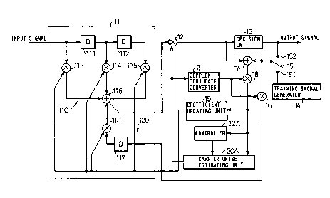
a filter unit 11.
The filter unit 11 comprises a feed-forward filter
110 composed of unit delay operators 111, 112, complex coef-
ficient multipliers 113, 114, 115, and a complex adder 116,
and a feedback filter 120 composed of a unit delay operator
117 and a complex coefficient multiplier 118.
An output signal from the complex adder 116, i.e.,
a filter output signal (aOf, bo~) from the feed-forward
filter 110, is supplied to a complex multiplier 12 which
multiplies the filter output signal by a reversely rotating
unit vector representlng an estimated carrier offset that is
estimated by a carrier offset estimating unit 20A for
- 27 -
A
21~0~81
thereby canceling out a carrier offset contained in the
output signal from the filter unit 11.
The complex multiplier 12 supplies its output sig-
nal to a decision unit 13 that determines which phase angle
range of the equation (2) the distorted phase angle of the
output signal from the filter unit 11 falls in. The
decision unit 13 then outputs a signal having the I and Q
components with a standardized phase angle expressed by the
equation (2).
The output signal from the decision unit 13 is
also supplied to a terminal 152 of a selector switch 15, and
subtracted from the output signal from the complex
multiplier 12 by a complex subtractor 17, thus producing an
equalization error signal. The equalization error signal is
a vector having, as its phase angle, the difference between
the above distorted phase angle and the standardized phase
angle expressed by the equation (2).
A training signal generated by a training signal
generator 14 is supplied to the other terminal 151 of the
selector switch 15. The selector switch 15 can thus select
the training signal from the training signal generator 14 or
the output signal from the decision unit 13.
The reversely rotating unit vector representing
the estimated carrier offset estimated by the carrier offset
estimating unit 20A is supplied to a complex conjugate con-
verter 21 as well as the complex multiplier 12. The complex
conjugate converter 21 converts the supplied unit vector
- 28 -
21iO881
into its conjugate complex signal, which is supplied to a
complex multiplier 16 that multiplies the supplied conjugate
complex signal by the output signal from the decision unit
13, thereby reversely correcting the corrected signal which
has been corrected based on the estimated carrier offset by
the complex multiplier 12, i.e., introducing the carrier
offset again. The complex multiplier 16 supplies its
reversely corrected output signal to the unit delay operator
117 of the feedback filter 120.
The equalization error signal from the complex
subtractor 17 is also supplied to a complex multiplier 18,
which multiplies it by the output signal from the complex
conjugate converter 21, thereby inversely correcting the
equalization error signal which has been corrected based on
the estimated carrier offset by the complex multiplier 12,
i.e., introducing the carrier offset again. The complex
multiplier 18 supplies its inversely corrected output signal
to a coefficient updating unit 19. The coefficient updating
unit 19 updates the coefficients of the coefficient
multipliers 113 ~ 115, 118 of the filter unit 11.
The output signal from the complex multiplier 18
is also applied to a controller 22A and also the carrier
offset estimating unit 20A. The controller 22A accumulates
the levels of equalization error signals for a certain
period of time to monitor the operation of the adaptive
equalizer. If the accumulated error is smaller than a
predetermined value, then the controller 22A determines that
- 29 -
2~881
the adaptive equalizer is operating normally, and turns on a
switch 200A (see FIG. 2). If the accumulated error is in
excess of the predetermined value, then the controller 22A
determines that the adaptive equalizer is malfunctioning,
and turns off the switch 200A thereby stopping the
estimating operation of the carrier offset estimating unit
20A.
As shown in FIG. 2, the carrier offset estimating
unit 20A comprises the switch 200A, an equalization error-
to-phase converter 201A for converting the inversely
corrected equalization error signal supplied from the
complex multiplier 18 through the switch 200A into a phase
quantity, an accumulator/adder 202A for accumulating and
adding phase quantities converted by the equalization error-
to-phase converter 201A, an accumulator/adder 203A for
accumulating and adding output signals from the
accumulator/adder 202A, and a phase-to-vector converter 204A
for convérting an output signal from the accumulator/adder
203A into a reversely rotating unit vector having a
corresponding phase angle and supplying the reversely
rotating unit vector to the complex multiplier 12.
The carrier offset estimating unit 20A operates as
follows: The inversely corrected equalization error signal
supplied from the complex multiplier 18 through the switch
200A, i.e., a signal containing noise in the transmission
path, phase and amplitude variations due to fading, and a
phase rotation due to the carrier offset, is converted into
- 30 -
2110881
a phase quantity by the equalization error-to-phase
converter 20lA.
Then, signals indicative of phase quantities from
the equalization error-to-phase converter 201A are accumu-
lated and added by the accumulator/adder 202A. When the
signals indicative of phase quantities are accumulated and
added for a certain period of time, the accumulated values
of noise in the transmission path and phase and amplitude
variations due to fading become zero, and the phase rotation
due to the carrier offset amounts to an angular velocity ~s~
Output signals from the accumulator/adder 202A are
also accumulated and added by the accumulator/adder 203A for
the time of a one-symbol interval, and converted into a
phase rotation quantity k-~s per symbol (k represents the
time of the one-symbol interval).
The phase rotation quantity k-~s is then converted
by the phase-to-vector converter 204A into a unit vector
which has the phase rotation quantity and is reversely
rotating. Thereafter, the reversely rotating unit vector
is supplied to the complex multiplier 12, which reversely
rotates the phase of the output signal from the filter unit
11 to cancel out the carrier offset.
If the input signal contains an excessive carrier
offset and cannot be corrected by the output signal from the
carrier offset estimating unit 20A, and the equalization er-
ror signal supplied to the controller 22A exceeds a
predetermined level, then the controller 22A applies a
- 31 -
-
2~08~1
control signal to turn off the switch 200A. At this time,
the carrier offset estimating unit 20A outputs a unit vector
having a phase angle that has been estimated in the
preceding slot.
As described above, the adaptive equalizer accord-
ing to the first embodiment of the present invention compen-
sates for a distorted component, i.e., a fading component,
produced in the transmission path, and also estimates a car-
rier offset from the e~ualization error signal and corrects
the output signal from the filter unit based on the
estimated carrier offset. The adaptive equalizer can thus
compensate for a phase rotation caused by the carrier offset
which results from the difference between the frequencies of
the detecting carrier and the transmitted carrier in the
quadrature detector, for thereby preventing the bit error
rate from being deteriorated by the carrier offset.
In estimating the carrier offset, the distorted
component that varies with time in the transmission path is
removed by accumulation and addition for a certain period of
time for extracting a phase quantity based on the carrier
offset. Consequently, the carrier offset estimating unit is
relatively simple in arrangement.
2nd Embodiment:
FIG. 4 shows an adaptive equalizer according to a
second embodiment of the present invention. Those parts
shown in FIG. 4 which are identical to those shown in FIG. 1
are denoted by identical reference numerals and will not be
- 32 -
2110881
described in detail below.
As shown in FIG. 3, an input signal applied to the
adaptive equalizer according to the second embodiment com-
prises a training signal 2 and data 3. As shown in FIG. 4,
the training signal 2 and the data 3 are stored in a buffer
memory 23. Then, the training signal stored in the buffer
memory 23 is read and supplied to a digital modulator 24,
which digitally modulates the training signal with carrier
frequencies at the interval of a predetermined frequency ~f
within a carrier offset range of from - fOff to ~ fOff which
is intentionally added. The digital modulator 24 outputs
and applies the digital modulated signal to a terminal 251
of a selector switch 25, which can select the modulated
signal.
After the training signal is read a predetermined
number of times from the buffer memory 23, the training sig-
nal and the data stored in the buffer memory 23 are read and
supplied to the complex multiplier 12, which multiplies them
by estimated corrective data (described later on). The com
plex multiplier 12 supplies its output signal to the other
terminal 252 of the selector switch 25, which can select the
output signal from the complex multiplier 12. The digital
modulated signal from the digital modulator 24 or the output
signal from the complex multiplier 12, which is selected by
the selector switch 25, is supplied to the filter unit 11.
The filter unit 11 is identical to the filter unit
11 according to the first embodiment. The output signal
21108~1
from the filter unit 11 is applied to the decision unit 13
that determines the phase of the output signal from the
filter unit 11. The decision unit 13 supplies its output
signal to the terminal 152 of the selector switch 15.
The training signal generated by the training sig-
nal generator 14 is supplied to the terminal 151 of the se-
lector switch 15. The selector switch 15 can thus select
the training signal from the training signal generator 14 or
the output signal from the decision unit 13.
The selected output data from the selector switch
15 are fed back to the unit delay operator 117, i.e., the
feedback filter 119 of the filter unit 11. The selected
output data from the selector switch 15 is also subtracted
from the output data from the filter unit 11, thus producing
equalization error data. The equalization error data are
supplied to the coefficient updating unit 19, which updates
the coefficients of the coefficient multipliers 113 ~ 115,
118 of the filter unit 11, i.e., updates the filter coeffi-
cients based on the equalization error data.
The equalization error data are also supplied
through a terminal 271 of a selector switch 27 to an equal-
ization error calculator/memory 26. The equalization error
calculator/memory 26 has a calculating unit for adding
equalization error data with respect to all symbols supplied
to the digital modulator 24 for each of the carrier
frequencies, and a memory unit for storing the sum for each
of the carrier frequencies.
- 34 -
21 1088:~
The sum of equalization error data stored in the
equalization error calculator/memory 26 is read into a car-
rier offset estimating unit 20B, which detects the minimum
value of the sum, converts the detected minimum value into a
phase angle, and adds the converted phase angle each time a
symbol is read, for conversion into a unit vector with the
converted phase angle. The carrier offset estimating unit
20B supplies the unit vector as corrective data to the com-
plex multiplier 12 in synchronism with the reading of the
symbols.
The selector switches 25, 15, 27 are controlled by
a control circuit 28 to shift in different patterns in dif-
ferent modes (described below).
Operation of the adaptive equalizer according to
the second embodiment will be described below with reference
to Tables 1 through 4 below.
When the input signal 1 having a format as shown
in FIG. 3 is supplied to the buffer memory 23, it is stored
in the buffer memory 23. An initializing mode and a carrier
offset estimating mode for the filter unit 11 are carried
out using the training signal 2, and an adaptive equalizing
mode is carried out using the training signal 2 and the data
3 according to the sequences described below. As described
above, the range of carrier frequencies intentionally
applied to the digital modulator 24 is the same as the range
(- fOff to ~ fOff (Hz)) of the carrier offset which the
received series of symbols is supposed to suffer, and the
- 35 -
211088:~
carrier frequencies change at the interval of the frequency
~f (Hz).
(a) First, the initializing mode is carried out.
The initializing mode and the carrier offset esti-
mating mode are related to each other as follows:
The filter coefficients are initialized with re-
spect to all the symbols of the training signal for one car-
rier frequency, and then the carrier offset estimating mode
is carried out with respect to all the symbols of the train-
ing signal for the same carrier frequency. Thereafter, the
carrier frequency is varied by the frequency ~f, and then
the filter coefficients are initialized and the carrier
offset estimating mode is carried out.
Table 1 below shows the manner in which the ini-
tializing mode is carried out.
- 36 -
~ Table 1
- Initializing mode 2110 8 8 1
Read sig- Training signal
nal
Carrier-foff -foff -foff +foff
frequency + ~f + 2~f
Operating Setting Updating, Updating, Updating, Updating,
phase I of FC Setting Setting Setting Setting
of FC of FC of FC of FC
Operating
phase II
Operating - - - - _
phase III
Connected 25: 251 25: 251 25: 251 25: 251 25: 251
terminals 15: 151 15: 151 15: 151 15: 151 15: 151
of SW 25, 27: Open 27: Open 27: Open 27: Open 27: Open
15, 27
FC: Filter coefficients
(a-0) During the initializing mode, the selector
switch 25 is connected to the terminal 251, the selector
switch 15 is connected to the terminal 151, and the selector
switch 27 is open under the control of the control circuit
28.
(a-1) The training signal of the input signal 1
stored in the buffer memory 23 is read and applied to the
digital modulator 24, which modulates the training signal
with a carrier frequency f. The modulated signal is
supplied to the filter unit 11, which removes an intersymbol
interference from the modulated signal by filtering.
2110881
(a-2) The output data from the filter unit 11 is
supplied to the complex subtractor 17, which calculates the
difference between the output data from the filter unit 11
and the training signal that is generated by the training
signal generator 14 depending on the training signal read
from the buffer memory 23, i.e., equalization error data.
(a-3) The equalization error data calculated by
the complex subtractor 17 are supplied to the coefficient
updating unit 19 thereby to update the filter coefficients
of the filter unit 17 based on the equalization error data.
(a-4) The training operation based on the carrier
frequency f is effected with respect to all the symbols of
the training signal. When the training operation is fin-
ished, the filter coefficients are converged.
The initializing mode based on the carrier fre-
quency f is followed by the carrier offset estimating mode
that is carried out at the carrier frequency f. Table 2 be-
low shows the manner in which the carrier offset estimating
mode is carried out.
- 38 -
21108~1
Table 2
Carrier offset estimating mode
Read sig- Training signal
nal
Carrier -fOff -fOff -fOff .................. +fOff
frequency + ~f + 2~f
Operating Setting Updating, Updating, Updating, Updating,
phase I of FC Setting Setting Setting Setting
of ~C of FC of FC of FC
Operating Accumu- Accumu- Accumu- Accumu- Accumu-
phase II lating, lating, lating, lating, lating,
adding of adding of adding of adding of adding of
equal- equal- equal- equal- equal-
ization ization ization ization ization
error error error error error
data data data data data
Operating Searching for minimum value ~
phase III Estimating phase angle
Connected 25: 251 25: 251 25: 251 25: 251 25: 251
terminals 15: 151 15: 151 15: 151 15: 151 15: 151
of SW 25, 27: 271 27: 271 27: 271 27: 271 27: 271
15, 27
FC: Filter coefficients
(b-O) During the carrier offset estimating mode,
the selector switch 25 is connected to the terminal 251, the
selector switch 15 is connected to the terminal 151, and the
- 39 -
2110881
selector switch 27 is connected to the terminal 271 under
the control of the control circuit 28. In the carrier
offset estimating mode, the filter coefficients obtained in
the initializing mode are used as initial values.
(b-1) The training signal of the input signal 1
stored in the buffer memory 23 is read and applied to the
digital modulator 24, which modulates the training signal
with a carrier frequency f. The modulated signal is
supplied to the filter unit 11.
(b-2) The output data from the filter unit 11 is
supplied to the complex subtractor 17, which calculates the
difference between the output data from the filter unit 11
and the training signal that is generated by the training
signal generator 14 depending on the training signal read
from the buffer memory 23, i.e., equalization error data.
(b-3) The equalization error data calculated by
the complex subtractor 17 are supplied to the coefficient
updating unit 19 thereby to update the filter coefficients
of the filter unit 17 based on the equalization error data.
(b-4) At the same time, the equalization error
data are supplied to the equalization error
calculator/memory 26, which calculates, in its calculating
unit, the sum of equalization error data with respect to all
the symbols at the carrier frequency f supplied to the
digital modulator 24. The calculated sum is stored in the
memory unit of the equalization error calculator/memory 26
with respect to the carrier frequency f supplied to the
- 40 -
2110881
digital modulator 24.
( c-O ) Then, the carrier frequency f is increased
by the frequency ~f . The initializing mode from ( a-O ) to
( a-4 ) is carried out at the frequency ( f + ~f ), and then the
carrier offset estimating mode from ( b-O ) to ( b-4 ) is
carried out at the frequency ( f + ~f ) .
( c-1 ) The above process is repeated as the carrier
frequency is varied from -fOff to +fOff at the interval ~f.
The stored contents of the equalization error cal-
culator/memory 26 upon completion of the above operation are
given in Table 3 below.
Table 3
Frequency f Accumulated and added equalization errors
- fOff a1
- f off + ~f a2
-fOff + 2~f a3
+fOff ~ ~f an+
+fOff an
(c-2 ) When the operation up to the carrier fre-
quency +fOff is over, the carrier offset estimating unit 22
searches for the minimum value of all accumulated and
added equalization error data stored in the equalization
error calculator/memory 26, converts the minimum value
into a phase angle based on a carrier frequency
-- 41 --
21~0881
corresponding to the minimum value, and converts the
converted phase angle into a unit vector having the
converted phase angle. The unit vector is sent as
corrective data to the complex multiplier 12. The unit
vector having the phase angle (-~) based on the minimum
value of all accumulated and added equalization error data
is sent as corrective data to the complex multiplier 12
for the reasons as follows:
If the input signal 1 has suffered an offset of
frequency f in the preceding stage, then the input signal
has been rotated by the phase angle ~. When the input
signal is modulated with a carrier frequency -f which
inversely gives a rotation by the phase angle (-~), the
output signal from the filter unit 11 becomes equal to the
training signal outputted from the training signal
generator 14, thus canceling the offset from the modulated
output signal.
Therefore, the input signal which has been
rotated by the phase angle ~ can be corrected by being
multiplied by the unit vector having a phase angle (-~1)
based on a frequency -f1 (~ -f) where the sum of
equalization error data is minimum.
Then, the adaptive equalizing mode is carried
out following the completion of the carrier offset
estimating mode. Table 4 below shows the manner in which
the adaptive equalizing mode is carried out.
- 42 -
211~8~1
Table 4
Adaptive equalizing mode
Read sig- Training signal Data
nal
Carrier - _
frequency
Operating Updating, Setting of FC Updating, Setting of FC
phase I
Operating Correction of each Correction of data with
phase II training signal with estimated phase angle
initial phase angle
Operating
phase III
Connected 25: 252 25: 252
terminals 15: 151 15: 152
of SW 25, 27: Open 27: 271
15, 27
FC: Filter coefficients
(d-O) During the adaptive equalizing mode, the
selector switch 15 is connected to the terminal 151 in a
training signal period under the control of the control
circuit 28, and the selector switch 15 is connected to the
terminal 152, the selector switch 25 is connected to the
terminal 252, and the selector switch 27 is open in a data
equalizing period under the control of the control circuit
28. In the adaptive equalizing mode, the filter
- 43 -
- 21iO881
coefficients obtained in the carrier offset estimating
mode are used as initial values.
(d-1) A training signal of the input signal 1
stored in the buffer memory 23 is read and applied to the
complex multiplier 12, which multiplies the training
signal by the initial unit vector as corrective data. The
corrected signal is then filtered by the filter unit 11.
(d-2) The output data from the filter unit 11 is
supplied to the complex subtractor 17, which calculates
the difference between the output data from the filter
unit 11 and the training signal that is generated by the
training signal generator 14 depending on the training
signal read from the buffer memory 23, i.e., equalization
error data.
(d-3) The equalization error data calculated by
the complex subtractor 17 are supplied to the coefficient
updating unit 19 thereby to update the filter coefficients
of the filter unit 17 based on the equalization error
data.
(d-4) Following training signals are
successively read, and the above process (d-1) ~ (d-3) is
effected until all the training signals are finished.
Each time the next training signal is read, the phase
angle of the unit vector is rotated by the phase angle of
the unit vector as the initial value in the carrier offset
estimating unit 20B. The unit vector whose phase angle is
multiplied by an integer is supplied as corrective data to
2110881
the complex multiplier 12, which multiplies the output
data from the filter unit 11 by the corrective data,
thereby correcting the output data from the filter unit
11 .
In the carrier offset estimating unit 20B, the
converted phase angle is added each time a symbol is read
because the phase angle of the input signal which has
suffered the carrier offset is incremented by the phase
angle ~ per input signal so that it varies from ~ to 2~ to
3~ .... In the adaptive equalizing mode, the phase angle
(-~1) of the corrective data, i.e., the unit vector, is
incremented by (-~1) each time the data is read from the
buffer memory 23 so that the phase angle varies from (-~1)
to (-2~1) to (-3~1) to (-4~1) ----
(d-5) After the reading of all training signals
is finished, the selector switch 25 is connected to the
terminal 152, and the data are successively read from the
buffer memory 23. The read data are corrected by being
multiplied by the unit vector which is rotated by the
phase angle ~1 each time the data is read and which is
outputted from the carrier offset estimating unit 20B, and
the corrected data are supplied to and filtered by the
filter unit 11.
(d-6) The output data from the filter unit 11
are supplied to the complex subtractor 17, which
calculates the difference between the output data from the
filter unit 11 and the output data from the decision unit
- 45 -
21~0881
13 to produce equalization error data.
(d-7) The equalization error data calculated by
the complex subtractor 17 are supplied to the coefficient
updating unit 19 thereby to update the filter coefficients
of the filter unit 17 based on the equalization error data
for an adaptive equalizing process.
(d-8) The above operation is repeated until all
the data are read from the buffer memory 23.
Consequently, the carrier offset produced in the preceding
stage such as a radio transmission unit can be compensated
for.
In the adaptive equalizer according to the
second embodiment, as described above, signals, as a
carrier, having a plurality of frequencies in a
predetermined frequency range including an expected
carrier offset are successively modulated by the training
signals of the input signal that are read from the buffer
memory, and the modulated output signals are supplied to
the filter unit. Output signals produced by subtracting
the training signal outputted by the training signal
generator from the output signals from the filter unit are
added for each carrier frequency. The carrier frequency
corresponding to the minimum value of the sum output
signal is converted into a signal based on the carrier
frequency, and the input signal is equalized by the
converted signal. Therefore, the carrier offset which the
input signal has suffered can be compensated for to
- 46 -
211~ J
prevent the error rate from being deteriorated.
3rd Embodiment:
FIG. 5 shows an adaptive equalizer according to
a third embodiment of the present invention.
The adaptive equalizer according to the third
embodiment differs from the adaptive equalizer according
to the second embodiment in that the complex multiplier 12
of the second embodiment is dispensed with, and the
carrier offset estimating unit 20B of the second
embodiment is replaced with a carrier offset estimating
unit 20C and a voltage-controlled oscillator 29 which
controls an oscillating frequency with the sum of a
voltage outputted from the carrier offset estimating unit
20C and a voltage applied from another source (not shown),
the voltage-controlled oscillator (VC0) 29 serving as a
local oscillator in a frequency conversion stage or a
quadrature-detection carrier oscillator. The other
details of the adaptive equalizer according to the third
embodiment are identical to those of the adaptive
equalizer according to the second embodiment.
The carrier offset estimating unit 20C is of the
same arrangement as the carrier offset estimating unit
20B. The carrier offset estimating unit 20C searches for
a minimum frequency and converts the minimum frequency
into a corresponding voltage. The voltage thus produced
is maintained at a constant level irrespective of the
reading of the training signal and the data from the
- 47 -
21~08~1
buffer memory 23. The voltage is added to the voltage
applied from the other source, and the sum voltage is
applied as a control voltage to the voltage-controlled
oscillator 29.
The adaptive equalizer according to the third
embodiment operates in the same manner as the adaptive
equalizer according to the second embodiment with respect
to the initializing mode and the carrier offset estimating
mode. In the adaptive equalizing mode, however, the
converted voltage corresponding to the minimum frequency
is maintained at a constant level irrespective of the
reading of the training signal and the data from the
buffer memory 23, and added to the voltage applied from
the other source, and the sum voltage is applied as a
control voltage to the voltage-controlled oscillator 29
for controlling the oscillating frequency.
Therefore, the oscillating frequency of the
local oscillator in the frequency conversion stage is
corrected based on the voltage outputted from the carrier
offset estimating unit 20C to compensate for the carrier
offset.
Furthermore, the adaptive equalizer according to
the third embodiment converts the carrier frequency corre-
sponding to the minimum value of the sum output signal
into the unit vector having the phase angle based on the
carrier frequency, multiplies the input signal read from
the buffer memory by the converted unit vector, and
- ~8 -
2~10~81
supplies the product output signal to the filter unit.
The multiplication process compensates for the carrier
offset which the input signal suffers to prevent the error
rate from being deteriorated.
In addition, the adaptive equalizer converts the
carrier frequency corresponding to the minimum value of
the sum output signal into the voltage based on the
carrier frequency, and applies the converted voltage to
the local oscillator in the stage preceding the adaptive
equalizer. Consequently, the carrier offset which the
input signal is- subjected to is compensated for in the
stage preceding the adaptive equalizer to prevent the
error rate from being deteriorated.
4 th Embodiment:
FIG. 6 shows an adaptive equalizer according to
a fourth embodiment of the present invention.
According to the fourth embodiment, the buffer
memory 23 and the digital modulator 24 in the second
embodiment are incorporated in the adaptive equalizer
according to the first embodiment. The adaptive equalizer
according to the fourth embodiment includes a carrier
offset estimating unit 20D and a controller 22B which are
similar to the carrier offset estimating unit 20A and the
controller 22A, respectively, in the first embodiment, and
an equalization error calculator/memory 26 which is
similar to the equalization error calculator/memory 26 in
the second embodiment. The other components and their
- 49 -
2 1 ~
operation according to the fourth embodiment are identical
to those according to the first through third embodiments,
and will not be described in detail below.
The adaptive equalizer according to the fourth
embodiment additionally has an initial value estimating
unit 30. The initial value estimating unit 30 is supplied
with the sum of equalization error data added per
modulation frequency in the digital modulator 24 and
stored in the equalization error calculator/memory 26,
detects the minimum value of the sum, converts the
detected minimum value into a phase angle based thereon,
and outputs it as an initial phase angle.
As with the second embodiment, the adaptive
equalizer according to the fourth embodiment operates in
three modes, i.e., the initializing mode, the carrier
offset estimating mode, and the adaptive equalizing mode.
These modes are also identical to those according to the
second embodiment except for details which will be
described below.
During the initializing mode and the carrier
offset estimating mode with the training signals, the
carrier offset estimating unit 20D outputs a unit vector
(1 + jO), and the complex conjugate converter 21 generates
a unit vector (1 - jO). Therefore, during the
initializing mode and the carrier offset estimating mode,
the output signal from the filter unit 11 and the
equalization error signal outputted from the complex
- 50 -
2 1 1 088 1
~. .
subtractor 17 are not corrected or inversely corrected
with respect to the carrier offset, and the coefficients
of the filter unit 11 are set and updated (see Table 1).
The equalization error calculator/memory 26 does
not operate in the initializing mode, but operates in a
certain manner in the carrier offset estimating mode.
More specifically, in the range of modulation frequencies
from -fOff to +fOff in the digital modulator 24, the sum of
equalization error data is accumulated in the equalization
error calculator/memory 26 per frequency interval ~f.
After the sum has been accumulated in the entire
modulation frequency range, the initial value setting unit
30 detects the minimum value of the sum of equalization
error data stored in the equalized error calculator/memory
26 (see Tables 2 and 3). The initial value setting unit
30 also generates an initial phase angle (-~)
corresponding to the detected minimum value of the sum of
equalization error data.
Then, the adaptive equalizing mode is carried
out. The adaptive equalizing mode is composed of a former
stage which employs the training signals and a latter
stage which employs the data (see Table 4). In the
adaptive equalizing mode, the digital modulator 24 is
inactive, and the training signals or the data read from
the buffer memory 24 is supplied directly to the filter
unit 11. In the adaptive equalizing mode, the
equalization error calculator/memory 26 and the initial
r ~
21~0881
value setting unit 30 are also inactive. The carrier
offset estimating unit 20D does not output the unit vector
(1 + jO), but outputs a unit vector (described below).
In the former stage which employs the training
signals, the carrier offset estimating unit 20D outputs a
unit vector having an initial phase angle (-~) which has
been obtained in the carrier offset estimating mode, to
the complex multiplier 12. The complex multiplier 12
cancels out a phase angle ~ corresponding to the carrier
offset which has been estimated in the carrier offset
estimating mode. In the former stage, the coefficients of
the filter unit are updated using the training signals
where the estimated carrier offset is canceled out.
When the former stage is over, the selector
switch 15 is shifted to the terminal 152, the selector
switch 27 is closed, and the data are read from the buffer
memory 23. At this time, the adaptive equalizer according
to the fourth embodiment operates in the same manner as
the adaptive equalizer according to the first embodiment
except that the buffer memory 23 is involved. The carrier
offset estimating unit 20D also operates in exactly the
same manner as the carrier offset estimating unit 20A
according to the first embodiment.
Since the adaptive equalizer according to the
fourth embodiment employs the training signals to estimate
an initial value for a carrier offset correcting quantity,
it is possible to obtain corrective data within a short
- 52 -
21iO881
period of time even when the carrier offset is large.
Moreover, a carrier offset while a normal signal
is being received is corrected on the basis of a phase
quantity based on the carrier offset component, which
phase quantity is extracted by accumulating and adding
distorted components in the transmission path over a given
period of time. Consequently, the carrier offset
estimating unit is relatively simple in arrangement.
Although certain preferred embodiments of the
present invention has been shown and described in detail,
it should be understood that various changes and modifica-
tions may be made tnerein without departing from the scope
of the appended claims.
- 53 -