Note : Les descriptions sont présentées dans la langue officielle dans laquelle elles ont été soumises.
~ 2110891
ELECTRICAL INTERCONNECTS HAVING
A SUPPORTED BULGE CONFIGURATION
BACKGROUND OF THE INVENTION
1. Field of the Invention
The present invention relates to interconnects or
contacts for conductors in a flat electrical circuit and, in
particular, to such interconnects which have a pointed, serial
or continuous supported bulge configuration, such as one or
more upsets, e.g. V-shaped and hollow shaped, wrinkles, folds
and creases, in both one or more of the conductors in the
circuit and any insulation underlying the conductors at the
sites of the interconnects.
2. Description of Related Art and Other Considerations
The interconnection of the electronic components,
especially high density electronic components and printed
wiring boards, presents recurring problems for which
multitudes of solutions have been presented. Conventionally,
micro-connectors, because of their small sizes, reauire
soldering or other very expensive techniques. In particular,
most connectors cannot handle a 3 mil to 5 mil (0.0762 mm to
0.1270 mm) or smaller line width and spacing in an efficient
manner.
Accordingly, many conventional interconnection
systems utilize pads or electrically conductive dots as a
means of ~roviding the interconnection, such as is disclosed
in United States Patents ~o. 4,125,310 and 4,453,795. These
patents describe a plurality of generally resilient metallic
raised projections. In the latter patent, a resilient backup
mechanism is used to avoid overstressing and squashing of the
resilient projections or contacts beyond their elastic limit,
which overstressing precludes repeated mating and unmating of
connectors incorporating such projections. While these
terminations otherwise effectively and reliably interconnect
mating circuits, their manufacture can be difficult, time
2110891
consuming and costly. Furthermore, the manufacturing process
for forming such bumps is limited to a size of about 2 mil
(0.0508 mm) in diameter.
In addition, such bumps require proper support,
without placing them at haz~rd to delamination due to
outgassing from support materials during or after production
or to inattention to thermal matching with its surrounding
materials, or to possible electrical or chemical interaction
with the surrounding materials.
SUMMARY OF THE INVENTION
These and other problems are solved by the present
invention, which comprises an electrical connector for a flat
cable or circuit having contacts or interconnects formed as
a bulge arrangement or configuration. These bulge-type
contacts or interconnects are shaped to provide a pointed,
serial or continuous bulge configuration, such as one or more
upsets, wrinkles, folds and creases, e.g., V-shaped and hollow
shaped, both in one or more of conductors in the circuit and
in any insulation underlying the conductors. The shape of the
bulge configuration is maintained by a support, which also is
selected to match physically and chemically with materials
surrounding it.
More specifically, the bulge configurations result
from so forming the cable as to provide one or more bulges in
the circuit having concave and convex portions configured as
single upsets, or a series of single upsets, or a linear
bulge, e.g., having a V-shaped appearance, or a linear bulge.
The support is shaped in accordance with the bulge into which
it fits. Thus, it may comprise a dielectric resin for fitting
into the pointed upsets or an extending bar with a V-shaped
part, which respectively fits into the bulge concave portions
or portion. A backing may be applied to the underside of the
cable under the single upset, or the bar itself may be affixed
to the underside of the circuit by an adhesive or secured into
a mating bar on the upper side of the circuit.
21 1 08~
Accordingly, the bulge configuration may
comprise a series of upsets or a linear or curved
wrinkle, fold or crease extending in a pattern across
at least some of the conductors and the underlying
dielectric circuit material if only one side of the
conductors is exposed, although the conductor may be
exposed on both sides to enable, for example, a
plurality of the circuits to be stacked together and
their bulges to interfit and electrically
interconnect with adjacent bulges. The pattern may
extend across the width of the circuit in any desired
fashion, such as at right angles, diagonally,
undulating, e.g., as a '~V", curved, or arced.
Several advantages are derived from the present
invention. Line widths and spacing between lines of
less than 3 mil (0.0762 mm), e.g., 1 mil (0.0254 mm)
or less, are obtainable so that the cable may be
connected to a printed wiring board or a flexprint
circuit, without the need to utilize other
connectors, solder or welding. The resulting
interconnection scheme provides for a low weight, low
volume and low profile interconnection. The cost of
manufacturing such bump configurations is much lower
as related to those of prior connection systems.
Other aspects of this invention are as follows:
An electrical connector, capable of establishing
electrical contacts in flat circuits having line
widths and spacing of less than 3 mil, comprising:
a flat circuit having a smooth surface and
including electrical conductors whose line widths and
spacings may be less than 3 mil and which are
encapsulated in dielectric material;
said conductors having sites defining positions
of electrical interconnects and being free from said
dielectric material on at least that conductor
surface portion which is closest to the smooth
surface of said circuit; and
., ,~- '
,,~.
21 1 0891
_ 3a
a configuration, positioned at the sites,
defining at least one ridge-like deformation
extending across said circuit and both said
conductors and any dielectric material contiguous
thereto to define at least one ridged bulge in and
across said conductors, for elevating those portions
of said conductors and said dielectric material
contiguous therewith and adjacent thereto at the
sites above the smooth surface, and a support
supporting said bulge being electrically, physically
and chemically compatible with its surrounding
materials.
An electrical connector comprising:
at least two stacked together flat circuits,
each having a smooth surface and including electrical
conductors encapsulated in dielectric material and
which have sites defining positions of electrical
interconnects that are free from said dielectric
material on at least that conductor surface which is
adjacent to a-stacked one of said circuits; and
like configurations in each of said circuits,
each of said configurations being positioned at the
sites and defining at least one bulge in said
conductors, for elevating those portions of said
conductors at the sites above the smooth surface,
said bulge configurations having interfittable
concave and convex portions, to enable said
conductors which are free from said dielectric
material on both sides thereof and said bulge
conflgurations therein in each of said circuits to
interfit in electrical contact with one another when
said circuits are stacked together; and
a support which is electrically, physically and
chemically compatible with its surrounding materials
and which is fittable into one of said concave
portions at an outer face of said stacked together
2 1 1 089 ~
3b
circuits, for supporting said interfitted bulge
configurations.
An electrical connector capable of establishing
electrical contacts in flat circuits whose electrical
lines have widths and spacings therebetween of 3 mil
and less in dimension, comprising:
a flat circuit including electric conductors
encapsulated in dielectric material and having a
smooth surface, said conductors having sites defining
positions of electrical interconnects and being free
from said dielectric material on at least that
conductor surface portion which is closest to the
smooth surface of said circuit; and
a supported ridge-like bulge arrangement which
extends at least substantially across said circuit
and is positioned at the sites in both said
conductors and any of said dielectric material
underlying said conductors, and which includes ridge-
like deformations for elevating those portions of
said conductors at the sites above the smooth
surface.
A method for providing electrical interconnects
in a flat electrical circuit having a substantially
uniformly smooth surface and electrical conductors
which are sizable to 3 mil and less line width and
spacing and are encapsulated in dielectric material,
in which the conductors have sites defining the
positions of the electrical interconnects and being
free from the dielectric material on at least that
conductor surface portion which is closest to the
smooth surface of the circuit, comprising the step of
forming supported deformations which extend
substantially continuously across the circuit and in
both the conductors and any dielectric material
contiguous thereto for defining ridged bulges in the
smooth surface at and adjacent to the sites in the
conductors and any underlying and adjacent dielectric
., .~
21 1 08~1
- 3c
material for elevating those portions of the
conductors, which are free from dielectric material,
at the sites above the smooth surface.
A method for providing electrical interconnects
in at least two flat electrical circuits, each having
electrical conductors encapsulated in dielectric
material and a substantially uniformly smooth
surface, in which the conductors have sites defining
the positions of the electrical interconnects and
being free from the dielectric material on at least
that conductor surface portion which is closest to
the smooth surface of its circuit and the circuit
adjacent thereto, comprising the steps of:
forming supported bulges in the smooth surface
at the sites in the conductors and any underlying
dielectric material for elevating those portions of
the conductors, which are free from dielectric
material, at the sites above the smooth surface;
configuring the bulges of each of the circuits
with interfittable concave and convex shaped portions
for enabling the bulges of each of the circuits to
interfit in electrical contact with one another of
the bulges;
stacking the circuits together in such a manner
as to interfit the respective bulge portions threof,
thereby forming a stacked circuit arrangement; and
fitting a support into the concave portions at
an outer face of the arrangement for supporting the
interfitted portions of the bulges.
Other aims and advantages, as well as a more
complete understanding of the present invention, will
appear from the following explanation of exemplary
embodiments and the accompanying drawings thereof.
21 1 0891
- 3d
BRIEF DESCRIPTION OF THE DRAWINGS
FIG. 1 illustrates a corner of a chip and
multiple leaded flat circuit, such as a flexprint
circuit, extending therefrom with its contacts having
the bulge configuration of the present invention;
FIG. 2 is a side view in partial cross-section
of an arrangement, such as is illustrated in FIG. l;
FIG. 3 illustrates a further embodiment for
interconnecting a stack of chips and their flexprint
circuits, such as shown in FIGS. 1 and 2;
'~'
- 2110891
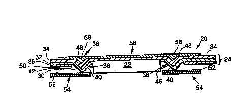
FIG. 4 is a top view of a flat cable arrangement;
FIG. 5 depicts the cable arrangement, such as shown
in FIG. 4, employing a bulge configuration having a linear or
curved pattern;
FIG. 6 is a top view of a flexible circuit with
individual bulge configurations on conductors therein;
FIG. 7 is a cross-sectional view of one of the bulge
configurations, such as depicted in FIG. 6;
FIG. 8 is an alternate arrangement of the bulge
configuration;
FIG. 9 depicts a method for forming one or more
bulge configurations; and
FIGS. 10a-lOd illustrate patterns of bulge
configurations extending across a cable.
DETAILED DESCRIPTION OF THE PREFERRED EMBODIMENTS
FIG. 1 illustrates a corner of an electronic
assembly 20 comprising a chip 22, a flexDrint circuit 24 and
supporting hardware 26. Flexprint circuit 24 includes a
plurality of fine lines, leads or conductors 28 which are
electrically connected to the chip and extend uDwardly to
electrical connecting points 30. The assembly thus far
described is of conventional construction, except that
connecting points 30 and their supports are configured in
accordance with the present invention.
As shown in FIG. 2, conductor 28, which is
illustrative of all conductors in flexprint circuit 24, is
imbedded within upper and lower layers 34 and 36 of dielectric
material, such as of polyimide plastic. A supported bulge
configuration 38, comprising individual bulges or upsets, is
formed at sites 40 on conductors 32 where contacts are
desired. These sites are produced by removal of plastic
insulation from lower plastic layer 36 to provide openings 42
therein. In the present invention, bulge configurations 38
are provided in both conductors 28 and underlying portions 44
of up?er plastic layer 3~. As shown, bulge configurations 38
- 21tO891
s
are V-shaped, having a convex portion 46 and a concave portion
48. The concave portion is of sufficient height that it
extends beyond the smooth surface, denoted by indicium S0, of
flexprint circuit 24. This extension of convex portion 46
S permits the exposed portion of conductor 28 to contact a
mating conductor 52 on another article 54, such as a
flexprint, printed wiring board, and a cable.
A support 56, having V-shaped protuberances 58, fits
within concave portions 48 of flexprint 24, to insure contact
between convex portions 46 and mating conductors 52. Support
56 may be formed of any rigid material, and may comprise a
metal, if the nletal is insulated from conductors 28, or a
rigid dielectric material. It is im~ortant that the material
of support 56 also be chemically compatible with the materials
constituting flexprint circuit.
The scheme shown with respect to FIG. 2 for a single
chip and flexprint circuit may be utilized for assembling a
plurality of chips and flexprint circuits into a stack, as
shown in FIG. 3. In this embodiment, the various elements are
substantially the same as that shown in FIG. 2 and, therefore,
are designated with the same numerals, but differentiated by
the addition of the letters ~a~ through ~d~ after the numeral,
in order to illustrate a plurality of flexprint circuits 24a,
24b, 24c and 24d, each having an upper plastic film 34a and
a lower plastic film 36a encapsulating electric conductors
32a. Because the intention in this embodiment is to
electrically couple all four chips of FIG. 3 into a stack at
interconnection sites 38a of the respective flexprint
circuits, insulation material from both upper layers 34a and
lower layers 36a are removed to provide respective openings
60 and 40a. The respective conductors 32a are bulged at sites
38a to provide V-shaped configurations, which define convex
portions 46a and concave portions 48a. These V-shaped
portions of conductor 32a are configured to be mutually
interfittable, so that all intermediate concave and convex
portions will contact. Support 56a having a V-shaped
~ 2110891
protuberance 58a is fitted into one of the concave portions
at an outer face 62 of the stacked together circuits. The
stacking of the V-shaped protuberances, in conjunction with
support 56a, provides support for all protuberances.
Referring now to FIGS. 4 and 5, a flexible circuit
or cable 64 comprises a plurality of conductors 66
encapsulated in plastic layers 68 and 70. Flexible cable 64
has smooth surfaces 72 and 74, with an opening 76 in surface
74 to define a site 78 for an interconnect. The interconnect
is formed by displacing a portion 80 of conductor 66 and an
underlying portion 82 of plastic layer 68. To insure that the
interconnect formed by portions 80 and 82 maintain their
shape, a support 84 having a V-shaped protuberance 86 is
positioned on smooth surface 72 of cable 64 and placed within
the concave portion of the interconnect. As illustrated in
FIG. 4, support 84 is maintained in contact with flexible
cable 64 by means of a cooperating plate secured to support
84 by fastening means such as screws 88 or to another plate
in contact with surface 74 of plastic layer 70.
FIGS. 6 and 7 illustrate the bulge configuration as
a sequence of pointed bulges or upsets 90 in a flat cable 92.
Cable 92 includes a plurality of electrical conductors 94
encapsulated between upper and lower plastic layers 96 and 98.
Material is removed from upper layer 96 to form an opening or
window 100 for exposing an upper surface 102 of conductor 94,
upper surface 102 being closest to the smooth surface, denoted
by indicium 104, of flexible cable 92 and its upper layer 96.
A pointed bulge is formed in each conductor 94 and its
underlying plastic portion 106 of lower layer 98 sufficient
to extend upper conductor surface 102 beyond smooth surface
104 of cable 92, in readiness for electrical contact with a
mating contact. A support 108, comprising a small amount of
rigid plastic, such as EPON 825 (a trademark of Shell Chemical
Company for a diglycidyl ether of Bisphenol A), is positioned
within the concave portion, designated by indicium 110, of
each upset 90. This EPON 825 rigid plastic is a preferred
- 2110891
material as meeting the several physical, electrical and
chemical criteria for a support. A backup film 112 or other
suitable layer is affixed to the surface, identified by
indicium 114, of lower layer 98 of flexible cable 92, to
assure that support 108 will remain in position.
In FIG. 8, which illustrates an alternate embodiment
of the present invention, a support 116 is configured with a
partial spherical surface 118 which interfits within a like
spherical concave portion 120 of a bulge confiquration 122.
FIG. 9 illustrates a method for forming a bulge
configuration and utilizes a tool 130. Tool 130 comprises a
die 132 and a blade 134. Die 132 has an opening 136 of width
W. Blade 134 has a thickness A and, preferably, terminates
in a rounded end 138. A flat cable 140 having a thickness B,
lS is positioned on die 132 and is so located that its opening
142 in a layer 143 of flat cable 140 defines a site 144 for
the interconnect to be formed. The relationships of the
dimensions of the tool and the cable is such that W = A + B
+ t, where t is a tolerance, for example of 0.005 inches
(0.127 mm), which is intended, in conjunction with rounded
blade end 138, to form a proper V-shaped bulge without
piercing or cutting into cable 140.
The bulge configurations of the present invention,
as shown FIGS. lOa-lOd, may take any suitable shape, whether
~ointed, serial or continuous, to form one or more upsets,
wrinkles, folds and creases in both one or more of the
conductors in the circuit or cable and in any insulation
underlying the conductors at the sites of the interconnects.
FIGS. lOa-lOd exemplify several paths of linear and curved
creases, folds or wrinkles. In FIG. lOa, bulge configuration
146 is patterned to take a path which extends linearly at an
angle or diagonal to conductors 148 of a cable 150. In FIG.
lOb, a bulge configuration 152 is patterned with a path which
extends at a sequence of lines 152a and 152b across conductors
154 of a cable 156. In FIG. lOc, bulge configuration 158 has
a pattern whose path gradually arcs across conductors 160 of
- 2110891
a cable 162. FIG. lOd illustrates a bulge configuration 164
formed as a semi-circle traversing conductors 166 of a cable
168. All of the bulge configurations shown in FIGS. lOa-lOd,
are supported by like-patterned supports.
Although the invention has been described with
respect to particular embodiments thereof, it should be
realized that various changes and modifications may be made
therein without departing from the scope of the invention.