Sélection de la langue

Search

Sommaire du brevet 2111433 

Énoncé de désistement de responsabilité concernant l'information provenant de tiers

Une partie des informations de ce site Web a été fournie par des sources externes. Le gouvernement du Canada n'assume aucune responsabilité concernant la précision, l'actualité ou la fiabilité des informations fournies par les sources externes. Les utilisateurs qui désirent employer cette information devraient consulter directement la source des informations. Le contenu fourni par les sources externes n'est pas assujetti aux exigences sur les langues officielles, la protection des renseignements personnels et l'accessibilité.

Disponibilité de l'Abrégé et des Revendications

L'apparition de différences dans le texte et l'image des Revendications et de l'Abrégé dépend du moment auquel le document est publié. Les textes des Revendications et de l'Abrégé sont affichés :

  • lorsque la demande peut être examinée par le public;
  • lorsque le brevet est émis (délivrance).
(12) Demande de brevet: (11) CA 2111433
(54) Titre français: FORMAT INTERNE ELARGI POUR CELLULE A MODE DE TRANSFERT ASYNCHRONE (MTA)
(54) Titre anglais: ASYNCHRONOUS TRANSFER MODE (ATM) EXPANDED INTERNAL CELL FORMAT
Statut: Réputée abandonnée et au-delà du délai pour le rétablissement - en attente de la réponse à l’avis de communication rejetée
Données bibliographiques
(51) Classification internationale des brevets (CIB):
  • H04J 03/08 (2006.01)
  • H04Q 11/04 (2006.01)
(72) Inventeurs :
  • DOMINIJANNI, DOMINIC (Etats-Unis d'Amérique)
  • PASHAN, MARK ALLEN (Etats-Unis d'Amérique)
(73) Titulaires :
  • AMERICAN TELEPHONE AND TELEGRAPH COMPANY
(71) Demandeurs :
  • AMERICAN TELEPHONE AND TELEGRAPH COMPANY (Etats-Unis d'Amérique)
(74) Agent: KIRBY EADES GALE BAKER
(74) Co-agent:
(45) Délivré:
(22) Date de dépôt: 1993-12-14
(41) Mise à la disponibilité du public: 1994-07-12
Requête d'examen: 1993-12-14
Licence disponible: S.O.
Cédé au domaine public: S.O.
(25) Langue des documents déposés: Anglais

Traité de coopération en matière de brevets (PCT): Non

(30) Données de priorité de la demande:
Numéro de la demande Pays / territoire Date
002,577 (Etats-Unis d'Amérique) 1993-01-11

Abrégés

Abrégé anglais


-7-
ASYNCHRONOUS TRANSFER MODE(ATM) EXPANDED
INTERNAL CELL FORMAT
Abstract
An ATM cell is formatted into an expanded internal cell format in order
to facilitate switched in a so-called "cell slice" memory based switching architecture.
Specifically, the ATM cells are expanded to the internal ATM cell format which is
matched to the throughput of the memory based switch architecture and the specific
bit assignments within the expanded ATM cell are matched to the cell slice
architecture. In one embodiment, the expanded ATM cells are each divided into a
plurality of parallel words which are, in turn, partitioned into so-called bundles. The
bundles correspond to the cell slice switch architecture with each bundle being
assigned to a particular portion of the switch architecture. (FIG. 1)

Revendications

Note : Les revendications sont présentées dans la langue officielle dans laquelle elles ont été soumises.


Claims:
1. Apparatus for generating expanded asynchronous transfer mode (ATM) cells
from a synchronous digital signal. for example, a SDH, SONET or the like digital signal,
having a predetermined clock rate and transporting ATM cells, comprising:
means for storing incoming ATM cells being transported by said synchronous
digital signal, said stored incoming ATM cells to be supplied as an output, each of said
incoming ATM cells having a predetermined number of bytes and each byte including a
predetermined number of bits;
means for increasing said number of bytes in said incoming ATM cells to be
supplied as an output to form internal ATM cells;
means for generating and inserting additional internal ATM cells to be supplied as
an output so that a clock rate equal to that of said incoming synchronous digital signal
clock rate may be used as a read clock for outputting said internal ATM cells from said
means for storing;
means for adding a predetermined number of bytes to said internal ATM cell to
form expanded ATM cells;
means for obtaining routing control information for each of said incoming ATM
cells;
means for inserting said routing control information for a particular incoming ATM
cell in predetermined bit positions of the added bytes in corresponding expanded ATM cell
transporting said particular incoming ATM cell; and
means for partitioning said bytes of said expanded ATM cells into a plurality ofpredetermined bundles, wherein said routing control information for said particular
incoming ATM cell is transported in a prescribed one of said bundles.
2. The apparatus of claim 1 wherein said predetermined number of bytes in said
incoming ATM cells is 53 bytes.
3. The apparatus of claim 2 wherein each of said internal ATM cells has 54 bytes.
4. The apparatus of claim 3 wherein each of said 54 byte internal ATM cells is
converted by a serial-to-parallel converter into a 48 bit parallel word.
5. The apparatus of claim 4 wherein said means for storing includes an elastic store
under control of a write controller so that nine of said 48 bit parallel words are
consecutively written into said elastic store during an ATM cell interval.

6. The apparatus of claim 5 wherein said means for expanding includes means for
reading out eight 56 bit parallel words from said nine stored 48 bit parallel words into
each of said expanded ATM cells.
7. The apparatus of claim 6 wherein each of said expanded ATM cells comprises a
20 bit header including two type bits. five reserve bits, an 8 by 8 control field, a 16 by 16
control field, six additional reserved bits, a 53 byte ATM cell, and four parity bits.
8. The apparatus of claim 7 wherein said means for obtaining routing control
information includes means for receiving a physical interface number from said incoming
ATM cells transported by said synchronous digital signal.
9. The apparatus of claim 8 wherein said means for obtaining routing control
information further includes means for generating a virtual path identifier value from said
56 bit parallel words read from said elastic store.
10. The apparatus of claim 6 wherein each of said expanded ATM cells is arrangedinto a sequence of 16, 28 bit parallel words wherein each 28 bit parallel word has 28 bit
positions.
11. The apparatus of claim 10 wherein said 28 bit parallel words are generated by
multiplexing said 56 bit parallel words.
12. The apparatus of claim 11 wherein said means for partitioning said bytes of
said expanded ATM cells into said plurality of predetermined bundles includes means for
shuffling said bits of said 16, 28 bit parallel words into said bundles.
13. The apparatus of claim 10 wherein a first of said 16, 28 bit parallel words
includes an expanded ATM cell header and a last of said 16, 28 bit parallel words includes
four parity bit positions.
14. The apparatus of claim 10 wherein said plurality of bundles includes a firstbundle, a second bundle, a third bundle, and a fourth bundle wherein said first bundle
includes bit positions 1 through 7 and bit position 25 of each of said 28 bit parallel words,
said second bundle includes bit positions 8 through 10 and bit position 26 of each of said
28 bit parallel words, said third bundle includes bit positions 11 through 17 and bit

position 27 of each of said 28 bit parallel words, and said fourth bundle includes bit
positions 18 through 24 and bit position 28 of each of said 28 bit parallel words.

Description

Note : Les descriptions sont présentées dans la langue officielle dans laquelle elles ont été soumises.


2 ~ 3
ASYN~HRONOUS TRANSFE~ MOD~: (AT~) E:~PANDED
INTERNAL CEI,L FO~MAT
Cross-Reference to Related Application
United States patent applicatis)ns SERIAL NO. (G.D. Martin- H. Ueda
5 Case 5-2) and SERIAL NO. (M.A. Pashan Case 6) were filed concurrently herewith.
Technical Fi~ld
This invention relates to digital transmission systems and/or switching
systems and, more particularly, to an ATM cell format.
Back~round of the Invention
In co-pending United States patent application Serial No. (M. A. Pashan
Case 6) a memory based switch arrangement is employed which requires the use of a
plurality of circuit cards in order to obtain desired cell buffer memory capacity. The
capacity is necessary in order to handle bursty data at high bandwidth and a low -
ATM cell loss rate. In order to eliminate the need of many bi-directional
15 communications links in such an arrangement, it is necessary to supply ATM cell
routing information to a controller in one of the circuit cards, which controller, in
turn, controls writing and reading of ATM cell data to and from cell buffer memory
on the master circuit card and cell buffer memory on a plurality of additional slave
circuit cards. This type of control of the additional slave circuit cards requires only
20 uni-directional communication links from the controller on the master card to the
cell buffer memory units on the additional slave circuit cards.
A problem that remains is to have an internal cell format that facilitates
such control and writing and reading of the ATM cell data.
Summary of the Invention
The elimination of the need to use numerous bi-directional
communications links in an enhanced cell buffer memory arrangement is facilitated,
in accordance with the invention, by employing an expanded internal ATM cell
format which is partitioned to supply all control information for data being supplied
to all of the circuit cards in the cell buffer memory arrangement, i.e., a master control
30 circuit card and a plurality of cell buffer memory slave circuit cards, directly ~o a
controller in the master circuit card and to supply predeterrnined other portions of
the expanded ATM cell directly to the plurality of slave circuit cards.
'~ '~ ` '~' ' .

3 ~
- 2 -
In an embodiment of the invention, an ATM cell is expanded to an
internal ATM cell forrnat matched to the throughput of the ATM memory based
switch arrangement and the specific bit assignments within the expanded ATM cellare matched to a so-called "cell slice architecture" of the memory based ATM switch
5 arrangement.
Specifically, each of the expanded ATM cells is divided into a plurality
of words, each word having a predetermined number of ~its. Then, each word is
partitioned into a plurality of bundles of bits corresponding to the memory based
ATM switch cell slice architecture. That is to say, each bundle is assigned to be
10 supplied to a predeterrnined one of the circuit cards in the memory based ATMswitch cell sliced architecture. Additionally, each bundle has an associated parity
check bit per expanded ATM cell. Initially, the plurality of parity check bits
corresponding to the plurality of bundles are in predeter nined bit positions of the
expanded ATM cell. The parity bits are then associated on a one-to-one basis, with a
15 corresponding one of the plurality of bundles and employed for fault isolation within
the circuit cards of the switching arrangement.
Brief Description of the Drawings
In the drawing:
FIG. I shows, in simplified block diagram form, an expanded ATM cell
20 formatter including an embodiment of the invention;
FIG. 2 shows an internal 54 byte ATM cell format useful in describing
the invention;
FIG. 3 shows an internal expanded 56 byte ATM cell format generated
in the formatter of FIG. 1.
FIG. 4 shows the expanded 56 byte ATM cell format of FIG. 3 arranged
in a sequence of 16, 28 bit parallel words; and
FIG. 5 shows the shuffled bits of each of the 28 bit words of FIG. 4 in
forming bundles.
Detailed Description
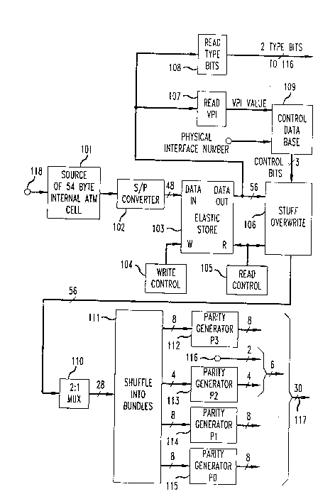
FIG. I shows a digital expanded ATM cell forrnatter 100 including an ~ ~
embodiment of the invention. Specifically, a digital transmission signal carrying
norrnal 53 byte ATM cells is supplied to the source of 54 byte internal ATM cell unit
101. This incoming digital signal may be anyone of a number of incoming digital
signals capable of transporting ATM cells in its payload portion. For example, the
35 digital transmission signal could be a digital synchronous hierarchy (SDH), signal or

2.~ 3 ~
- 3 -
a SONET digital signal. In this example, it is assumed that the ATM cells are being
transported in an STM- 1 SDH digital signal of a type known in the art. It is noted
that the standard 53 byte ATM cell is defined in CCITT Recommendation I.361,
entitled "B-ISDN ATM LAYER SPECIF~CATION" dated July, 1992 and the STM-
5 I digital signal format is described in CCITT Recommendation G.709, entitled"Synchronous Multiplexing Structure" dated 1988.
The output of source of 54 byte internal ATM cell unit 101 is a cell
structured as shown in F~G. 2. An arrangement for generating such an internal 54byte ATM cell format as shown in FIG. 2, is described in co-pending United States
10 patent application Serial No. (G. D. Martin-H. Ueda Case 5-2), filed concurrently
herewith. For brevity and clarity of exposition only a single ATM cell stream isshown and described. It will be apparent to those skilled in the art that a number
(e.g., 16) of such ATM cell streams may be combined, i.e., multiplexed together, for
internal processing. The internal 54 byte ATM cells are supplied from unit 101 to
15 serial-to-parallel (S/P) converter 102. S/P converter 102 converts the internal 54
byte ATM cell into parallel words, each having 48 bits. In turn, these 48 bit parallel
words are written into elastic store 103 under control of write control 104 such that
nine (9) consecutive 48 bit parallel words are written in during an ATM cell interval.
In turn, the stored bits of the internal 54 byte ATM cell are read out as 56 bit parallel
20 words under control of read control 105 during an ATM cell interval. In order to
expand the internal 54 byte ATM cell stored in elastic store 103 to an expanded 56
byte ATM cell, eight (8) 56 bit words are read out in an ATM cell interval. The first
56 bit parallel word being read out includes the two (2) type bits and two (2) reserve
(RSRV) bits from the internal 54 byte ATM cell shown in FIG. 2, 16 stuffed bits ~ ~
(i.e., 2 bytes) and 36 data bits. The next six (6) of the 56 bit parallel words transport ~ ~ -
ATM cell data, while the last parallel word transports 52 bits of data and includes 4
bit positions for parity check bits, to be described below.
This expanded 56 byte internal ATM cell is shown in FIG. 3. Note that
the expanded 56 byte ATM cell is comprised of a 20 bit header including the two (2)
type bits, then five (5) reserve (RSRV) bits, a "8 x 8" control field, a "16 x 16'1
control field (not important to this invention) and six (ff) additional reserved bits, 53
bytes including the standard ATM cell and four (4) parity bits.
Referring again to FIG. 1, the 56 bit parallel words being read from
elastic store 103 are supplied to stuff over~vrite unit 106, to read VPI (i.e., virtual
path identifier) unit 107 and to read type bits unit 108. It is noted that knowing the
specific physical interface number for the incoming signal and the ATM VPI value,
-- .. - . - . ~ , .

- ~ -
the destination of the ATM cells can be obtained from control data base 109. TheVPI value for a network-to-network interface AT~I cell structure is in the first 12
bits of the AT~I cell header, as defined in ~CITT Recommendation 1.361. That is,the routing control information for the ATM cell in the memory based ATM switch
S architecture can be obtained. In this particular example, the memory based ATMswitch architecture described in the above noted co-pending United States patentapplication Serial No. (M. A. Pashan Case 6) is an "8 x 8" switch having eight (8)
inputs and eight (8) outputs. Consequently, three bit positions are needed to carry
the routing control in~ormation. The three (3) control bits for the ATM cell are10 supplied to stuff overwrite unit 106, and under control of read control 105 overwrite
three (3) of the stuffing bit positions in the header of the expanded 56 byte ATM cell
format. This control field is shown as an "8 x 8" field in the header of the expanded
56 byte ATM format shown in FIG. 3. The 56 bit parallel words are then supplied
from stuff overwrite unit 106 to 2: I multiplexer (MUX) 110 to obtain 28 bit parallel
IS words. The 28 bit parallel words are supplied to shuffle into bundles unit 111 which
arranges the bits in each 28 bit word into predeterrnined bundles. FIG. S illustrates
the shuffling for word one (I) of ~he expanded 56 byte ATM cell. As shown in FIG.
4, it is noted that each expanded 56 byte ATM cell is comprised of 16, 28 bit parallel
words. The first word includes the expanded ATM cell header and the 16th word
20 includes four parity bit positions.
It should be noted that although FIG. S shows the first word as including
parity bit positions P0, Pl, P2 and P3, actual parity bits are only transported in word
16. As shown in FIG. S, bundle A includes bit positions I through 7 and bit position
25 of each word, bundle B includes bit positions 8 through I 0 and bit position 26 of - . ~-
25 each word, bundle C includes bit positions 11 through 17 and bit position 27 of each
word and bundle D includes bit positions 18 through 24 and bit position 28 of each
word. Bundle A is supplied as eight t~) parallel bits from shuMe into bundles unit
111 to parity generator P3 112. Bundle B is supplied as four (4) parallel bits from
shuMe into bundles unit 111 to parity generator P2 113. Bundle C is supplied as
30 eight (8) parallel bits from shuffle into bundles unit 111 to parity generator Pl 114.
Bundle D is supplied as eight (8) parallel bits from shuMe into bundles unit 111 to
parity generator P0 I IS. Each of parity generators 112 through I IS generates parity,
in known fashion, for its corresponding bundle A through bundle D, respectively,over the sequence of 16, 28 bit parallel words comprising the expanded 56 byte
35 ATM cell. Parity generators 112 through l lS supply as outputs bundles A through
D, respectively, as 28 bit parallel words. Each expanded 56 byte ATM cell, as noted

3 ~
above, comprises a sequence of 16 such 28 bit parallel words with the parity bit for
each bundle being transported in the 1 6th word only. Additionally, it is noted that
the two (2) type bits from read type bits unit 108 are supplied via 1 16 as an output
along with the four (4) bits in bundle B, thereby forming a six (6) bit bundle.
S Consequently, the parallel words being supplied as an output from expanded ATM cell forrnatter 100 via 1 17 are actually 30 bits parallel words.
The above-identified arrangements are, of course, merely illustrative of
the application of the principles of the invention. Other arrangements may be
devised by those skilled in the art without departing from the spirit or scope of the
1 0 invention.
.

Dessin représentatif
Une figure unique qui représente un dessin illustrant l'invention.
États administratifs

2024-08-01 : Dans le cadre de la transition vers les Brevets de nouvelle génération (BNG), la base de données sur les brevets canadiens (BDBC) contient désormais un Historique d'événement plus détaillé, qui reproduit le Journal des événements de notre nouvelle solution interne.

Veuillez noter que les événements débutant par « Inactive : » se réfèrent à des événements qui ne sont plus utilisés dans notre nouvelle solution interne.

Pour une meilleure compréhension de l'état de la demande ou brevet qui figure sur cette page, la rubrique Mise en garde , et les descriptions de Brevet , Historique d'événement , Taxes périodiques et Historique des paiements devraient être consultées.

Historique d'événement

Description Date
Inactive : CIB expirée 2013-01-01
Inactive : CIB de MCD 2006-03-11
Demande non rétablie avant l'échéance 1999-09-20
Inactive : Morte - Aucune rép. dem. par.30(2) Règles 1999-09-20
Réputée abandonnée - omission de répondre à un avis sur les taxes pour le maintien en état 1998-12-14
Inactive : Renseign. sur l'état - Complets dès date d'ent. journ. 1998-10-27
Inactive : Abandon. - Aucune rép dem par.30(2) Règles 1998-09-18
Inactive : Dem. de l'examinateur par.30(2) Règles 1998-03-18
Demande publiée (accessible au public) 1994-07-12
Toutes les exigences pour l'examen - jugée conforme 1993-12-14
Exigences pour une requête d'examen - jugée conforme 1993-12-14

Historique d'abandonnement

Date d'abandonnement Raison Date de rétablissement
1998-12-14

Taxes périodiques

Le dernier paiement a été reçu le 1997-10-23

Avis : Si le paiement en totalité n'a pas été reçu au plus tard à la date indiquée, une taxe supplémentaire peut être imposée, soit une des taxes suivantes :

  • taxe de rétablissement ;
  • taxe pour paiement en souffrance ; ou
  • taxe additionnelle pour le renversement d'une péremption réputée.

Les taxes sur les brevets sont ajustées au 1er janvier de chaque année. Les montants ci-dessus sont les montants actuels s'ils sont reçus au plus tard le 31 décembre de l'année en cours.
Veuillez vous référer à la page web des taxes sur les brevets de l'OPIC pour voir tous les montants actuels des taxes.

Historique des taxes

Type de taxes Anniversaire Échéance Date payée
TM (demande, 4e anniv.) - générale 04 1997-12-15 1997-10-23
Titulaires au dossier

Les titulaires actuels et antérieures au dossier sont affichés en ordre alphabétique.

Titulaires actuels au dossier
AMERICAN TELEPHONE AND TELEGRAPH COMPANY
Titulaires antérieures au dossier
DOMINIC DOMINIJANNI
MARK ALLEN PASHAN
Les propriétaires antérieurs qui ne figurent pas dans la liste des « Propriétaires au dossier » apparaîtront dans d'autres documents au dossier.
Documents

Pour visionner les fichiers sélectionnés, entrer le code reCAPTCHA :


Pour visualiser une image, cliquer sur un lien dans la colonne description du document. Pour télécharger l'image (les images), cliquer l'une ou plusieurs cases à cocher dans la première colonne et ensuite cliquer sur le bouton "Télécharger sélection en format PDF (archive Zip)" ou le bouton "Télécharger sélection (en un fichier PDF fusionné)".

Liste des documents de brevet publiés et non publiés sur la BDBC .

Si vous avez des difficultés à accéder au contenu, veuillez communiquer avec le Centre de services à la clientèle au 1-866-997-1936, ou envoyer un courriel au Centre de service à la clientèle de l'OPIC.


Description du
Document 
Date
(aaaa-mm-jj) 
Nombre de pages   Taille de l'image (Ko) 
Abrégé 1994-07-11 1 35
Dessins 1994-07-11 4 217
Revendications 1994-07-11 3 145
Description 1994-07-11 5 283
Dessin représentatif 1998-08-26 1 25
Courtoisie - Lettre d'abandon (R30(2)) 1998-11-15 1 171
Courtoisie - Lettre d'abandon (taxe de maintien en état) 1999-01-10 1 184
Taxes 1996-09-03 1 78
Taxes 1995-10-22 1 73
Taxes 1996-11-24 1 77
Demande de l'examinateur 1998-03-17 3 110
Correspondance de la poursuite 1994-03-13 3 53