Note : Les descriptions sont présentées dans la langue officielle dans laquelle elles ont été soumises.
CA
2 ~12180
-- 1 --
1 Electron Source and Manufacture Method of Same, and
Image Forming Device and Manufacture Method of Same -
BACKGROUND OF THE INVENTION ~ - -
Field of the Invention
The present invention relates to an electron
source for emitting an electron beam and a manufacture ;~
method of the electron source~ as well as an image -~
forming device such as a display for forming an image by
irradiation of an electron beam and a manufacture method
of the image forming device.
Related Background Art
Known hitherto are two kinds of electron
emitting elements, i.e., a thermo-electron source and
15 a cold cathode electron source. As a cold cathode -~
electron source~ there are electron emitting elements
of field emission type (hereinafter abbreviated as FE),
metal/insulating layer/metal type (hereinafter ;- -~
abbreviated as MIM)~ and surface conduction type.
Known as examples of FE are W.P. Dyke & W.W~
Dolan~ "Fieldemission", Advance in Electron Physics~
8, 89 (1956), C.A. Spindt, "Physical Properties of
thin-film field emission cathodes with Molybdenium
cones"~ J. Appl. Phys.~ 47~ 5428 (1976), etc.
Known as examples of MIM are C.A. Mead, "The
tunnel-emission amplifier"~ J. Appl. Phys.~ 32~ 646
(1961), etc.
~ 2:~12~8~
-- 2 --
Known a5 examples of an electron emitting element
of surface conduction type are M.I. Elinson, Radio Eng.
Electron Phys.~ 10 (1965), etc. ;
Here~ the term "electron emitting element of
surface conduction type" means an element which utilizes
a phenomenon of causing electron emission when a thin - ~ -
film of small area is formed on a base plate (substrate) -
and a current is supplied to flow parallel to the film --~
surface. As electron emitting elements of surface
conduction type~ in addition to the above-cited element ~;
by Elinson using an Sn~2 thin film~ there have been~
reported an element using an Au thin film [G. Dittmer~
"Thin Solid Films"~ 9~ 317 (1972)]~ an element using an
In2O3/SnO2 thin film [M. Hartwell and C.G. Fonstad~
"IEEE Trans. ED Conf."~ 519 (1975)3, an element using -
a carbon thin film [Hisashi Araki et. al.: "Vacuum"~ i
Vol~ 26~ No~ 1~ pO 22 (1983)]~ etc. -
As a typical element configurat~ion of those ~ }
electron emitting elements of surface conduction
type~ Fig. 28 shows a configuration of the above
element reported by M. Hartwell et. al. In Fig. 28
denoted by 231 is an insulating base plate and 232 lS
an electron emitting portion forming thin film which
is of a thin film of metal oxide or the like formed
;~ 25 by~ sputtering in~o a H-shaped pattern. An electron
emltting portion 233 is formed by an electrifying
process called 'forming' described later. 234 is
: ' - '''
~' 2 ~ 0
-- 3
-~'
1 referred to as an electron emitting portion including
thin film.
In such an electron emitting element of surface
conduction type, it has conventionally been general to
form the electron emitting portion forming thin film
232 into the electron emitting portion 233 beforehand
by an electrifying process called 'forming' prior to
start of electron emission. The term 'forming' means
a process of by applying a voltage across the electron
emitting portion forming thin film 232 to effect an
electrifying process so that the electron emitting
portion forming thin film is locally broken, deformed
or denatured, thereby forming the electron emitting
.. ::: . ...
portion 233 which is caused to have an electrically --
high-resistant state. With the electron emitting
element of surface conduction type thus subjected to ~ ~
the 'forming' process, electrons are emitted from the - ~-
electron emitting portion 233 by applying a vol~age to
the electron emitting portion including thin film 234
and flowing a current through the element.
However, the above prior art electron emitting
elements of surface conduction type have~ accompanied
various problems in realizing practical use. Therefore,
the applicant has conducted intensive studies alming
at various improvements and has solved the problems in
practical use as follows.
For example 7 the applicant has proposed a novel
, . , . ,, . , . . . . . - . . ... . ,, .. ,. ~ ,
2 ~
- 4 -
1 electron emitting element of surface conduction type
that, as shown in Fig. 27, a ~ine particle film 244 is
arranged as the electron emitting portion forming thin
film between electrodes 242 and 243 on a base plate
241, and the fine particle film 244 is subjected to ;~
the electrifying process to form an electron emitting
portion 245 (Japanese Patent Application Laid-Open
No. 2-56822).
As an example in which numerous electron
emitting elements of surface conduction type are formed
in an array, there have been proposed an electron ~-
source having a number of rows in each of which
electron emitting elements of surface conduction type
are arrayed in parallel and these individual elements ; ~ ~ ~
15 are interconnected at their both ends by wires (e.g., - ~ -
Japanese Patent Application Laid-Open No. 64-31332
filed by the applicant).
Meanwhile, particularly in the field of image
sensing devices including displays, flat type displays
using liquid crystals have recently been prevented in
place o~ CRT's. But liquid crystal displays are not -
emission type and hence have had such a problem as ! '
requiring backlights or the like. For this reason,
displays of ~m; ~sive type have been demanded.
In order to satisfy such a demand, a disylay in
combination of an electron source which comprises an
array of numerous electron emitting elements of surface
... -- ,
S~ ~ ~2183
1 conduction type, and a fluorescent material which
emanates a visible light upon impingement of electrons
emitted from the electron source has been proposed as
an image forming device (e.g., U.S. Patent No 5,066,883
assigned to the applicant). This is an emissive type
display which enables even a large-screen device to
be relatively easily manufactured, and which is
superior in display quality.
In a variety of image forming devices including
the above-mentioned display, a larger screen size and
higher fineness are inevitably demanded and expected.
However, for an electron source in which numerous
electron emitting elements are formed into an array as
mentioned above, the following problems, for example,
may be caused due to troub~es particularly encountered
in manufacture:
1) defect or failure of electron emitting
elements themselves,
2) disconnection of common wires or short
circuit between adjacent wires, and
3) failure of interlayer insulation in areas
where common wires cross each other.
SUMMARY OF THE INVENTION
An object of the present invention is to deal
with the aforesaid problems occurred in an eleatron
source, in which numerous electron emitting elements
- 2~12~
- 6 -
l are formed into an array, due to troubles encountered
in manufacture, especially a defect or failure of ;
electron emitting element themselves, and to remarkably
improve a production yield of electron sources and ~-
image forming devices.
Also, an object of the present invention is to ~ ~
:. ~'," ~.' :
provide an electron source and a manufacture method of
the same, and an image forming device and a manufacture
method of the same, by which a defect or failure of
electron emitting element themselves can be coped with
sufficiently, and deterioration of image quality such
as pixel defects and uneven brightness occurred when
images are displayed is very small.
Further, the present invention is concerned -
with an electron source comprising numerous electron
emitting elements, particularly electron emitting
elements of surface conduction type, formed into an
array, and an image forming device using such an
electron source, and its object is to increase a
production yield and improve deterioration of image
~uality.
According to an aspect of the present invention, ~ ~
there is provided an electron source comprising a base - ~-
plate and an electron emitting element disposed on the
base plate, wherein:
the electron emitting element includes a
plurality of electron emitting portions electrically
-' 2~2~
- 7 ~
1 connected in parallel~ the electrical connection being
made through a thermally cut-off member.
According to another aspect of the present
invention, there is pxovided a manufacture method for
S an electron source comprising a base plate and an : .
electron emitting element disposed on the base plate,
comprising the steps of:
forming a pluraltiy of electron emitting
portions electrically connected in parallel on the
base plate,
checking the plurality of electron emitting
portions to detect electron emission characteristics,
and
cutting off the electrical connection in that
electron emitting portion on which the electron
emission characteristic has been found not normal as
a result of the checking step. I -
According to still another aspect of the present
invention, there is provided an electron source~ ~:
comprising a base plate and an electron emitting~ ~ :
element disposed on the base plater wherein: -
the electron emitting element includes an .
electron emitting portion connected to voltage supply
means through a thermally cut-off member, and an
electron emitting portion forming film which includes -~-
a thermally connecting member.
According to still another aspect of the :~
--~ 2 ~ 0 -;
- 8 -
1 present invention, there is provided a manufacture
method for an electron source comprising a base plate
and an electron emitting element disposed on the base
plate, comprising the steps of~
forming an electron emitting portion connected
to voltage supply means, and an electron emitting
portion forming film on the base plate,
checking the electron emitting portion to
detect an electron emission characteristics, and : .
cutting off the connection in that electron ~:
emitting portion on which the electron emission ~ :
characteristic has been found not normal as a result
of the checking step~
connecting the electron emitting portion forming
film to the voltage supply means, and
forming an electron emitting portion in the
electron emitting portion forming film. -
According to still another aspect of the
present invention, there is provided an electron ~ -~
20 source comprising a base plate and an electron ~ ~-
emitting element disposed on said base plate~
wherein~
said electron emitting element includes an ~ ~:
: electron emitting portion connected to voltage supply :.:
25 means, the connection being performed by using a -
thermally connecting member. -~
According to still another aspect of the ~:
f~
- 9 - :
1 present invention, there is provided an image forming
device comprising any of the above electron sources,
an image forming member for producing an image upon
irradiation of electron beams emitted from the electron
s source, and modulation means for modulating the
electron beam irradiated to the image forming member
in accordance with an input image signal.
BRIEF DESCRIPTION OF THE DRAWINGS
Fig. l is a schematic view for explaining an
embodiment of an electron source according to a first
aspect of the present invention.
Fig. 2 is a perspective view showing a practical
configuration of an electron emitting element of -
15 sur~ace conduction type used in the embodiment of the ;
electron source according to the first aspect of the
present invention.
Figs. 3A to 3H are views of successive steps ~ -
for expla; n~ ng a method of manufacturing the electron;~ -
20 emitting element of surface conduction type shown in ~;
Fig. 2.
Fig. 4 is a chart showing one example of a
.: -
voltage waveform applied to carry out an electrification
'forming' in the manufacture step for the electron
emitting element of surface conduction typeO
Fig. 5 is a diagram showing an evaluation
device for evaluating an outpl1t characteristic of the
--~ 2 ~ 1 8 0
-- 10 --
l electron emitting element of surface condition type.
Fig~ 6 is a graph showing examples of an output
characteristic of the electron emitting element of
surface condution type according to the electron source
5 of the presen~ invention. ~
Fig. 7 is a perspective view showing the electron -
emitting element of surface conduction type, in which
electrical connection is cut off in an electron
emitting portion being not normal, for the electron
source according to the first aspect of the present
invention.
::
Fig. 8 is a perspective view showing a practical ~ ~ ~
:-:, , ~"::
configuration of an electron emitting element of
sur~ace conduction type used in another embodiment of
the electron source according to the first aspect of
the present invention. --
Fig. 9 is a schematic view for explaining ~ -~
another embodiment of the electron source according to - ~
the first aspect of the present invention. ~-
Fig. 10 is a schematic view for explaining -
still another embodiment of the electron source -
according to the first aspect of the présent invention.
Fig. ll is a schematic view of a display using ;; ~-
-: . .,:: ,
the electron sources according to the first aspect of
- . ~ .
; 25 the present invention. -~ ~
, - ,-:
Fig. 12 is a simplified block diagram for
explaining a driver circuit of the display shown in ~ ;
. - ::~'
~ \
- 11 - 2 ~
1 Fig. 11.
Fig. 13 is a schematic view for explaining
still another embodiment of the electron source
according to the first aspect of the present invention.
Fig. 14 is a schematic view for explaining
still another embodiment of the electron source
according to the first aspect of the present invention.
Fig. 15 is a schematic view of a display using
the electron sources shown in Fig. 14.
Fig. 16 is a simplified block diagram for -~
explaining a driver circuit of the display shown in
Fig. 14.
Fig. 17 is a schematic view for expla; n; ng an -~
embodiment of an electron source according to a second
.
lS aspect of the present invention.
Fig. 18 is a perspective view showing one
practical configuration of an electron emitting - -
element of surface conduction type according to the
electron source shown in Fig. 17. -
Fig. 19 is a perspective view showing an
example in which an electron emitting portion is
formèd by subjecting a portion B of the electron
~emitting element of surface conduction type shown in
:: ~
;~ Fig. 18 to 'forming'.
Fig. 20 is a perspective view showing another
configuration of the electron emitting element of
surface conduction type shown in Fig. 17.
21~21~
- 12 -
1 Fig. 21 is a schematic view of a display using
the electron sources shown in Fig. 17.
Fig. 22 is a schematic view for explaining
another embodiment of the electron source according to
the second aspect of the present invention.
Fig. 23 is a perspective view showing one
practical configuration of an electron emitting element
of surface conduction type shown in Fig. 22.
Fig. 24 is a schematic view for explaining
still another embodiment of the electron source
according to the second aspect of the present invention.
Fig. 25 is a schematic view for explaining still
another embodiment of the electron source according to --
the second aspect of the present invention.
: :: ::: :.
Figs. 26A to 26F are plan views showing examples
of a defect or failure occurred in the electron
emitting element of surface conduction type.
Fig. 27 is a plan view showing one eX~mple of ~-
prior art electron emitting elements of surface
20 conduction type. ~ -
Fig. 28 is a plan view showing another example ~ ~ -
of prior art electron emitting elements of surface !
conduction type.
:.::. ' .' :
25 DESCRIPTION OF THE PREFERRED EMBODIMENTS : :~
Of the above-mentioned troubles possibly
occurred in manufacture of an electron source and an
- 13 - 2~121~
1 image forming device in which numerous electron
emitting elements are formed into an array, a defect
or failure of eleetron emitting elements may appear
as follows:
a) electrieal short circuit (defect),
b) electrical disconneetion (defeet), and
c) unsatisfactory characteristic of electron ~ ;
emission (failure).
As a result of eondueting intensive studies on -
such a defect or failure of electron emitting elements,
the inventors have diseovered the following interest
finding about electron emitting elements, especially -
eleetron emitting elements of surfaee eonduetion type
(often referred to simply as "surfaee eonduetion electron
emitting elements"). The diseovered f;nrling will be
deseribed with referenee to Figs. 26A to 26F.
Figs. 26A to 26F are plan views looking from
above at a base plate on whieh an eleetron emitting
element of surface eonduetion type is provided, and
showing a state before a 'forming' proeess whieh is
to be made to form an electron emitting portion.
First, an eleetric short cireuit possibly
oecurred in the eleetron emitting alement of surfaee
eonduction type is caused upon a eonduetive substanee
bridging between element electrodes 225 and 226, for
example, as shown in Fig. 26A. If sueh a bridge is
produeed, it is naturally resulted that a voltage
121~
- 14 -
1 cannot effectively be applied to an electron emitting
portion forming thin film 224 and the 'forming' ~:~
process (i.e., electrifying process for the electron
emitting portion forming thin film 224) or actual .
5 driving cannot be effected. -~
The above bridge is mainly attributable to the
fact that proper etching has not been carried out .
owing to dust deposited.on a photoresist or local
unevenness of etchant density, for example, when the :.
element electrodes 225, 226 are formed by .
photolithography etching As another case, when an
electrode pattern is formed by lif.t-off, the bridge
may be produced if washing after the lift-off is not
sufficient and a peeled flake is left in such a state : ~:
. .. . :-
as to straddle both the element electrodes 225, 226. .~
- -
Then, an electrical disconnection possibly .~
:
occurred in the electron emitting element of surface .
conduction type is caused when an electrical
connection between the element electrodes 225, 226, :~:
including the electron emitting portion forming thin
film 224 formed therebetween, is cut off at any :~
location, for example, as shown in Figs. 26B and 26C.
If such a disconnection occurs, it is also naturally : -~
resulted that a voltage cannot effectively be applied
to the electron emitting portion forming thin film 224
and the 'forming' process or actual driving cannot be
effected.
2~ 3
- 15 -
1 The electrical disconnection as shown in Fig.
26B is often caused upon such an occasion, for example, -
that a mask pattern is shifted in its position during
a step of forming the electron emitting portion forming
s thin film 224, or the electron emitting portion forming
thin film 224 is partly peeled off after the formation ~-
thereof.
Also, the electrical disconnection as shown in
Fig. 26C is often caused upon such an occasion, for
example, that the element electrodes 225, 226 include
defects developed in their film forming, or they are
partly peeled off after the film forming. ~-
An unsatisfactory characteristic of electron
emission possibly occurred in the electron emitting
element of surface conduction type is caused when the
above electrical short circuit or disconnection happens
to such an extent as not leading to a fatal defect as
shown in Figs. 26D to 26F. In this case, since a
voltage or an electric field or electric energy
effectively applied to the electron emitting portion
forming thin film 224 is deviated from a preset design
value, application of the voltage in thè 'forming'
process or actual driving cannot be effected as
intended, which remarkably reduce an emitted current
(i.e., an output electron beam).
- The present invention has been made principally
based on the finding explained above. Hereinafter,
2 ~ 0
- 16 -
1 preferred embodiments of the present invention will be
described in detail. ~ ; -
The inventors have solved the above-mentioned
problems in an electron source and an image forming
device each including electron emitting elements,
especially electron emitting elements of surface
conduction type, by using two means below.
With the first means of the present invention,
a plurality of electron emitting portion forming thin
film are provided in electrically parallel beforehand
on each electron emitting element of surface conduction
type, and electron emitting portions are formed by
carrying out an electrification '~orming'.
Characteristics of the formed electron emitting
portions are then checked. Those electron emitting
portions which have good characteristics are used as
they are, but for those electron emitting portions on
which unsatisfactory characteristics or defects have
been found, the electrical connection is cut off
completely. The number of the electron emitting
portions having good characteristics for each - --
i
electron emitting element is stored in a memory, and
a drive signal is modified based on data read out of -~
the memory when the electron emitting element is -~-
driven.
Thus, with the first means of the present
invention, a probability of causing complete element
~'~ '' ~" ''
2~121~
- 17 -
1 defects can be made very small by providing a plurality
of electron emitting portion forming thin films for
each element. In addition, since the driving is
modified depending on the number of good electron
5 emitting portions, variations in output of electron
beams for the electron emitting elements can also
be made very small.
With the second means of the present invention
an electron emitting portion forming thin film
electrically connected to wiring electrodes beforehand
and an electron emitting portion forming thin film
not yet electrically connected to wiring electrodes
are both provided on each electron emitting element of
surface conduction type, the former thin film being
subjected to the electrification 'forming'. A
characteristic of the electron emitting portion
formed by the electrification 'forming' is then checked.
When the characteristic is good, that the electron
emitting portion is used as it is. However, if an
unsatisfactory characteristic or defect is found, the
electrical connection between that electron emitting
portion and the wiring electrodes is cut off completely.
Thereafter, the spare electron emitting portion forming
thin film not yet electrically connected is now ~ -
connected to the wiring electrodes and then subjected
to the electrification 'forming~.
Thus, with the second means of the present ~ -
- 18 -
1 invention, even if the electron emitting portion first
subjected to the electrification 'forming' is found -
as having a drawback, it can be replaced by the spare
electron emitting portion forming thin film and,
therefore, a production yield of electron emitting
elements of surface conduction type can drastically
be improved.
The spare electron emitting portion forming thin
film is not necessary the same in shape as the electron -
emitting portion forming thin film electrically
connected beforehand. In view of spatial restrictions,
the spare electron emitting portion forming thin film
may be formed to have a smaller size. In this case,
driving modification means is provided for modifying a
difference in the electron emission characteristic due
to different sizes or shapes. By providing such means,
an electron beam can be produced substantially at the
same output in the case of using the spare electron
emitting portion forming thin film as well. -
The above-mentioned two means of the present
invention may be practiced solely or in combination of -
the both.
The present invention is preferably applicable
to, in particular, electron emitting elements of
surface conduction type. It has been proved that the
present invention is extremely effective when applied
to elements having electron emitting portions below.
~ ,~ ~' ''' ''
19 - ~ ~1 121~
1 An electron emitting portion in an electron emitting
portion including thin film is formed by conductive
fine particles of which grain size is several tens
angstroms, and the r~ n;ng electron emitting portion
including thin film is formed of a fine particle film.
The term "fine particle film" used herein means a
film which is formed as an aggregation of many fine
particles, and of which fine structure includes not
only a condition where individual fine particles are
dispersedly arranged, but also a condition where fine
particles are adjacent to or overlapped with each
other (including insular aggregations).
In other cases, the electron emitting portion
including thin film may be a carbon thin film or the
like dispersed with conductive fine particles.
The electron emitting portion including thin
film is practically formed of, for example, any of
metals such as Pd, Ru, Ag, Au, Ti, In, Cu, Cr, Fe, Zn,
Sn, Ta, W, Nb, Mo, Rh, Hf, Re, Ir, Pt, Al, Co, Ni, Cs, -~
Ba and Pb, oxides such as PdO, SnO2, In2O3, PbO and
Sb2O3, borides such as HfB2, ZrB2, LaB6, CeB6, YB4
and GdB4, carbides such as TiC, ZrC, HfC, TaC, SiC
and WC, nitride such as TiN, ZrN and HfN, semiconductors - -
such as Si and Ge, as well as carbon and the like. -
The electron emitting portion including thin .
film is formed by any of such methods as vacuum :~
evaporation, sputtering, chemical vapor deposition,
~'; '- : .
- 20 - 2 ~ a
l dispersion coating, dipping, and spinning.
The present invention will be described below
in more detail in connection with embodiments. ~
[Embodiments] --
To begin with, a first aspect of the present
invention will be described with reference to F~gs. 1
to 16.
According to the first aspect of the present
invention, an electron source is basically arranged
such that at least a plurality of electron emitting
portion forming thin films are provided in electrically
paxallel for each electron emitting element, and
electron emitting portions are formed in these thin ;~
films. In the case of an electron emitting element of
surface conduction type, for example, the electron
emitting portions are formed respectively in the
electron emitting portion forming thin films by -~
carrying out an electrification 'forming'.
Characteristics of the formed electron emitting ;~
20 portions are then checked. For those electron emitting -~
portions which exhibit unsatisfactory characteristics,
the electrical connection is cut of~ completely to
disable application of a drive signal. Further, a ~-
drive signal is modified in accordance with the
number of good electron emitting portions in each
element.
- 21 - 2~21~
[ Embodiment 1 ]
Fig. 1 is a schematic view showing one embodiment
of an electron source according to the first aspect of
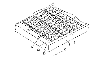
the present invention. In Fig. 1, a reference numeral 1
denotes a base plate (substrate) and an area 31 defined
by dotted lines schematically represents one of numerous
electron emitting elements of surface conduction type
which are formed on the base plate 1. Only nines of
those numerous elements are illustrated in Fig~ 1.
Each electron emitting element of surface
conduction type includes, as constituent members,
three portions indicated by A in Fig~ 1 (hereinafter
referred to as portions A) and three portions indicated
by h~tched areas 32 (hereinafter referred to as ~ -
thermally cut-off portions). More specifically, the
portion A represents an electron emitting portion and
surroundings thereof, and the thermally cut-off portion
32 represents a member which has good conductivity ~-
at the room temperature, but which is changed into an -~
electrically insulated state by being molten or
oxidi~ed when heated. Note that the portion A and the
thermally cut-off portion 32 iIlustrated in adjacent '
relation schematically indicate that both the members ~;~
are electrically connected in series, and these two
members are not always spatially adjacent to each
other.
As shown in Fig. 1, one electron emitting
,"','''' '''"
'-'.'- ~'~.
2 ~ ~ ~
_ 22 -
1 element of surface conduction type comprises total
three sets of the portions A and the thermally cut-off
portions 32 which are electrically connected in series
in each se~, the three sets being electrically connected
in parallel. Also, 33 and 34 schematically represent
common wires for electrically connecting the electron
emitting elements of surface conduction type in
parallel which are arrayed in the X direction.
The electron emitting element 31 of surface
conduction type will now be described in more detail.
Fig~ 2 is a perspective view for explaining a ~ -
structure of the electron emitting element of surface
conduction type. In Fig. 2, denoted by 1 is a base ~
plate formed of soda lime glass, for example, and 33, ~ ~-
34 are common wiring electrodes made of Ni, for example.
An area 31 defined by dotted lines corresponds to one
electron emitting element of surface conduction type.
Also, 41, 43a, 43b, 43c and 45 are electrodes made of
Ni, for example. Electron emitting portion forming
thin films 42a, 42b, 42c are provided respectively
between the electrode 41 and the electrodes 43a, 43b, -~ ~
43c. Further, electron emitting portions 3a, 3b, 3c ~; .'
are formed respectively in the electron emitting ~;
portion forming thin films 42a, 42b, 42c by an
electrification 'forming' described later.
The portion A shown in Fig. 1 corresponds to
a portion in Fig. 2 constituted by, for example, the
2l~2.~a
- 23 -
1 electron emitting portion forming thin film 42a, the
electron emitting portion 3a, the electrode 43a, and
a part of the electrode 41. On the other hand, thin
films 44a, 44b, 44c made of In2O3, for example, are
provided respectively between the electrode 45 and
the electrodes 43a, 43b, 43c in Fig. 2, these thin
films 44a, 44b, 44c corresponding to the thermally
cut-off portions 32 in Fig. 1.
The thin films used to form the thermally cut-
off portions are preferably made of such material as
above-cited In2O3, for example, which has good
conductivity at thie room temperature, but which is -;
easily evaporated, molte~ or deformed when heated.
Dep~n~;ng on cases, ITO on the like may be used in
place of In2O3. Alternatively, such material as Al,
for ~Amrle~ which has good conductivity at the room
temperature, but which is easily oxidized to provide a
very high electrical resistance when heated.
In the electron emitting element of surface
conduction type described above, a drive voltage is
applied to the electron emitting portions 3a, 3b, 3c
through the common wiring electrodes 33, 34 for
emanating electron beams from the electron emitting
portions.
A method of manufacturing the electron emitting -
element of surface conduction type shown in Fig. 2 will
be described below in detail.
- 24 _ ~121~
1 Figs. 3A to 3E~ are views for expalining steps
of manufacturing the electron emitting element of
surface conduction type, each figure showing a section
of the base plate taken along line B - B' in Fig. 2.
5 Note that, for convenience of illustration, Figs. 3A -~
to 3H are all drawn on an arbitrary reduction scale.
[Step-l]
On the base plate 1 of soda lime glass
sufficiently cleaned with pure water, a detergent and ;~
an organic solvent, a pattern 51 was formed by using
a photoresist (RD 2000N-41, by Hitachi Chemical, Co.,
Ltd.). Thereafter, 50-angstrom thick Ti and 1000
angstrom thick Ni were successively laminated by
vacuum evaporation (Fig. 3A).
[Step-2]
Then, the photoresist pattern Sl was dissolved
with an organic solvent to partially remove the Ni/Ti
deposited film by liftoff, thereby forming the
electrodes 41, 43b, 45 each made of Ni/Ti. In this
embodiment, a gap G between the electrodes 41 and
43b was set to 2 microns (Fig. 3B)
[Step-3]
Between the electrodes 43b and 45, an In2O
film 44b was formed in thickness of 1000 angstroms by
vacuum film forming and photolithography (Fig. 3C).
[Step-4]
A mask pattern 52 for producing the electron
- 25 _ 2 1 :l 2 ~ ~ ~
1 emitting portion forming thin film was formed as a
Cr film being 1000 angstroms thick and deposited by
vacuum evaporation (Fig. 3D).
[Step-5]
With the base plate being rotated by a
spinner, an organic Pd solution (CCP4230, by Okuno
Pharmaceutical Co., Ltd.) was coated over the base
plate and then baked, thereby forming a thin film 53
of Pd fine particles (Fig. 3E).
10 [Step-6] .
The Cr film was subjected to wet etching with
an acid etchant to selectively remove a lamination of
the thin film 53 and the Cr deposited film by liftoff,
whereby the electron emitting portion forming thin
15 film 42b was produced (Fig. 3F). .
., :::.,
[Step-7]
The electron emitting portion forming thin . -:~
film 42b was then subjected to an electrification ' ~. :
'forming'. More specifically, a predetermined :~
20 'forming' voltage was supplied between the electrodes ~ --
41 and 45 by a 'forming' power supply 54, causing a
current to flow through the electron emitting portion
forming thin film 42, whereby the electron emitting
portion 3b was formed. By the electrification
'forming', the electron emitting portions 3a, 3c were
also formed respectively in the electron emi~ting ~
portion forming thin films 42a, 42c at the same time ~ :
~ 26 - 2~12~
l (Fig. 3G).
Fig. 4 shows one example of thie predetermined -~ :
'forming' voltage.
The 'forming' voltage is given as triangular
5 wave pulses with Tl of 1 mlllisecond, T2 of lO ~ '~
milliseconds, and a peak voltage of 5 [V]. The pulses
having such a waveform were applied for 60 seconds -
under a vacuum atmosphere of l x lO 6 [Torr]. In this -~
way, the electron emitting portion 3b is formed in a
10 part of the electron emitting portion forming thin : -~
film 42b under a condition that fine particles each
cont~;n;ng a palladium element as a main ingredient -.
are dispersedly arranged in the electron emitting
portion 3b. A mean grain size of the fine particles was
30 angstroms.
Note that the 'forming' voltage is not limited ~ -
to the aforesaid waveform, but it may have any suitable
other waveform such as a rectangular waveform, for
example. Also, a peak value, pulse width, pulse :
interval, etc. of the 'forming' voltage are not
necessarily limited to the above-cited values, but
may have any suitable values so long as the electron
emitting portion is formed successfully. ~-
[Step-8]
The electron emitting element 31 of sur~ace
conduction type shown in Fig. 2 was fabricated through
the foregoing steps. However, because the electron
27 - 2~
1 emitting portions are not always formed successfully
in all the electron emitting portion forming thin
films as suggested relating to the Related Background
Art, a characteristic of electron emission was then ~-
checked.
Fig. 5 shows one schematic configuration of a
measurement/evaluation device for checking an electron ;~
emitting characteristic of the electron emitting ~
element of surface conduction type. --
In Fig. 5, denoted by 71 is a power supply ~ -
for applying an element voltage Vf, i.e. a driving ~ ; ~
voltage applied to an electron emitting element, to ~ ~ -
the electron emitting element of surface conduction
type, 72 is an anode electrode for capturing an
emission current Ie emitted from the electron emitting
element of surface conduction type, 73 is a high~
voltage power supply for applying a voltage to the ~ ~ ~
anode electrode 72, and 74 is an ammeter for measuring -
the emission current Ie. The electron emitting
element of surface conduction type and the anode
electrode 72 are installed in a vacuum apparatus
which is provided with equipment such as an exhaustion
pump and a vacuum gauge (not shown) necessary for
measurement and evaluation under a desired vacuum.
Actual measurement and evaluation were made
on condition that a voltage applied to the anode
electrode by the high-voltage power supply 73 was set
21l21 8~
- 28 -
1 to the range of 1 ~kV] to 10 [kV] and a distance H
between the anode electrode and the electron emitting
element of surEace conduc~ion type was set to the
range of 3 [mm] to 8 [mm].
Fig. 6 shows an output characteristic of the
electron emitting element of surface conduction type
measured by the above measurement/evaluation device.
Note that since an absolute value of the output
characteristic depends on a size and shape of the
10 element, a characteristic graph of Fig. 6 is plotted ~-
in an arbitrary unit.
When the three electron emitting portions 3a,
3b, 3c of the electron emitting element of surface
conduction type are all good, the emission current Ie
15 exhibits a characteristic indicated by (lj in Fig. 6. ~ ;
When any twos of the three electron emitting
portions are good, the Ie exhibits a characteristic
indicated by (2) in Fig. 6. Further, when only one
of the three electron emitting portions is good, the
Ie exhibits a characteristic indicated by (3) in
Fig. 6.
If the threé electron emitting portions are
all not good although this rarely happens in terms
of probability, the emission current Ie is not
appreciably detected. In this case, the relevant
~lement is not used. But if a failed portion can be
repaired, that element is checked again after the
r~~ 2 ~ a
~ 29 ~
1 repair. If a failed portion is difficult ~o restore
by repair, it is preferable to reuse that element as
raw material from the standpoint of environment
and resources.
According to the present invention, when the
electron emission characteristic is as indicated by
(1), that element is used as it is. However, when -
the electron emission characteristic is as indicated ~ ~
by (2) or (3), one or two thermally cut-off portions - -
electrically connected to the failed electron
emitting portions in series are selectively heated ~
so as to burn out or cut off the electrical connection ~ ;
therebetween. -
The process up to the above disconnection will
now be described.
For the electron emitting element of surface
conduction type on which the electron emission
characteristic has been found as indicated by (2) or
(3), a check is performed by a method of using image -
processing in order to discriminate which one(s) of
the three electron emitting portions 3a, 3b, 3c is
good and which one(s) of them includes a failure or
defect. As explained before with reference to the
examples of Fig. 27, the electron emitting portion
forming thin film including a failure or defect has a
configurational feature such as a chip or projection
in its surroundings. This feature is still left after
~'
_ 30 _ ~li21~3
1 the electrification 'forming'. Therefore, the good
electron emitting portion can easily be discriminated
from one includin~ a failure or defect based on their
configurations.
In practice, the check is performed by using,
for example, an image sensing device such as an
: ~ ~
industrial TV camera provided with a magnifying lens,
image memories and an image processor. More
specifically, the image of the electron emitting
element of surface conduction type is picked up by
the image sensing device, and image data is once
stored in one image memory. On the other hand, an
image pattern of the normal element is stored in
another image memory beforehand. The image processor
lS executes a pattern matching between the normal image
pattern and the sensed image data and, when the both
are matched with each other, it determines that
element to be normal.
The subsequent step will be described on an
assumption that the electron emission characteristic
was found as indicated by (2) in Fig. 6 and the normal
electron emitting portion was not formed in the
electron emitting portion forming thin film 42b as a
result of the determination made based on the check
method using image processing
[Step-9]
In this embodiment, the thermally cut~off
2~ a , , ~
- 31 - --
l portion 44b connected to the abnormal electron
emitting portion in series was selectively heated by
a laser beam, ~or example, thereby cutting oEf the
electrical connection therebetween.
- :.: .. :.
More specifically, as shown in Fig. 3H, the
thermally cut-off portion 44b was locally irradiated
with a laser beam from a laser source 54 so that it
was molten to cut off the electrical connection. The
laser sourc~ 54 can be any of infrared lasers such as
a carbon dioxide laser, Co laser and YAG laser, for
example. It is only required for the laser source to
be able to produce a relatively high power and easily
effect heating. Other than irradiating the laser
beam directly to the thermally cut-off portion 44b as
shown in Fig. 3H, a transparent member may be
interposed between the laser source and the portion
44b, or as shown in the drawing by the broken line, the - -
laser beam may be irradiated from the lower surface
side of the glass base plate l depending on cases.
One electron emitting element of surface
conduction type in the electron source of this
embodiment manufactured as explained above is shown
in Fig. 7.
[Embodiment 2] --
The construction of the electron emitting
~ ,.. :.
elements of the electron source according to the -~
first aspect of the present invention is not limited
';';~"';'~' '
- 32 - ~ 0
; '';''
1 to that described above with reference to Figs. 2 ~ -
to 7. The thermally cut-off portion is not
necessarily separated from the electron emitting
portion forming thin film. In accordance with the
basic concept of the first aspect of the present
invention, a part of the electron emitting portion
forming thin film may also serve as the thermally cut-
off portion.
Fig. 8 is a view for explaining such an
embodiment. In this embodiment, electron emitting
portion forming thin films 102a, 102b, 102c are
formed between the electrodes 41 and 45, and a
scattering preventive member 101 is provided between
adjacent twos of the electron emitting portion forming
thin films.
As with the embodiment of Fig. 7, Fig. 8 is
drawn on an assumption that central one of the three
electron emitting portions was not normally formed.
Instead of the thermally cut-off portion 44b in Fig. 7,
a part of the electron emitting portion forming thin
film 102b is irradiated with a laser beam to cut off -
the electrical connection this embodiment. ! ' :
The scattering preventive member 101 is ~
provided to prevent, when the electron emitting portion ;
forming thin film is heated by a laser beam, fragments
of the thin film from scattering to the adjacent
normal electron emitting portions and adversely
_ 33 _ 2 1 1 2 ~ ~ ~
. , -,. :,
1 affecting them. The scattering preventive member
101 can be formed of the same material as the
electrodes 41, 45, but it is more effective by
setting a thickness to be not less than 1 micron,
for example.
[Embodiment 3]
The construction of the electron source
according to the first aspect of the present invention
is not limited to that schematically shown in Fig. 1. ~
The number of the electron emitting portions ~ -
provided electrically in parallel for each element
is not limited three. It is important that plural
electron emitting portions are provided in each
element. For example, each element may include six
electron emitting portions. Also, the electron
emitting portions are not necessarily arranged in a
line.
As schematically shown in Fig. 9, for example,
one element 31 may include six portions A electrically
connected in parallel, these six portions A being
spatially arranged in two rows each comprising three
portions A. Alternatively, as schematically shown
in Fig. 10, one element 31 may include two portions
A.
~ ' ':, '
~ 34 ~ 2112~0
~ .
1 [Embodiment 4]
In thi.s embodiment~ a description will be given
of one example of an image display using the electron
source shown in Fig. 10. Fig. 11 is a schematic
view showing a display panel of the image display of
this embodiment.
Referring to FigO 11~ denoted by 1 is a base
~ plate of the electron source, Gl, G2, G3 are grid
electrodes for modulating respective electron beams,
and 133 is a face plate of the display panel.
Fig. 11 shows an area including only nine
pixels in the display panel comprised of numerous
pixels. The face plate 133 and the base plate 1
double as a part of a vacuum vessel ~not shown)~
and a vacuum level of about 10 6 ~Torr], for example~
is maintained inside the vessel. Also, the face ~ : :
plate 133 is constituted by forming a transparent
electrode 13I formed of an ITO thin film, for
example, and a fluorescent material 132 on an inner
surface of a base plate 130 made of glass, for
example. Depending on cases, a metal back well
known in the art of CRT may be provided at the ..
underside of the fluorescent material 132.
A voltage of 10 ~kV], for example, i~
applied to the transparent electrode 131 by a high-
voltage power supply (not shown), and the fluorescentmaterial 132 emanates a visible light upon irradiation
-
- 35 - 2~12~
1 o~ an electron beam.
The grid electrodes Gl, G2, G3 are each a stripe-
shaped electrode fabricated by machining a thin plate
of metal material, for example, and provided with ~ ~ ;
openings 135 in alignment with the corresponding the
electron emitting elements of surface conduction type
so that electron beams pass through the electrodes.
The grid electrodes are electrically independent of
one another and, by changing the magnitude of a
modulation voltage externally applied to each of the
grid electrodes, the intensity of an electron beam
passing through the opening 135 and irradiating the
fluorescent material can be controlled. Also, by
changing the time length (duration) of a modulation -~
lS voltage pulse, the amount of charges of an electron
beam passing through the opening 135 and irradiating '
the fluorescent material can be controlled. -
: ~ . .:
Accordingly, by adjusting the magnitude of the ~
:: . . , . :-
modulation voltage applied to the grid electrode or
20 the duration of the modulation voltage pulse, the ~ ;~
lllm;n~nce of a light emanated from the fluorescent
material can freely be controlled.
Further, similarly to the electron source shown
in Fig. 10, numerous electron emitting elements 31 of
25 surface conduction type (see Fig. 10) are formed into -
an array on the glass base plate 1. The electron
emitting elements of surface conduction type arrayed in
- 36 - ~ ~ 2 ~ ~ ~
1 the X direction are interconnected electrically in
parallel. Denoted by 33d, 34d, 33e, 34e, 33f in
Fig. 11 are common wired electrodes for establishing
such parallel connection.
In the display panel of this embodiment,
rows of electron emitting elements of surface
conduction type formed to array in the X direction
and columns of stripe-shaped grid electrodes ~ormed
to extend in the Y direction cooperatively form an ~;
XY matrix. Stated otherwise, by applying a suitable
drive ~oltage to one of the common wired electrode ~
pairs, any one of the element rows can selectively ~ -
be driven, and by applying suitable modulation
signals to the grid electrodes at the same time,
electron beams emitted from that element row can be
modulated individually. As a result, by successively -~
changing over the elements rows to be driven, all
pixels tdenoted by 134 in Fig. 11) of a display
screen can be scanned in turn~
Fig. 12 is a simplified block diagram showing
an electric circuit configuration for driving the
display panel of Fig. 11 in accordance with an image
signal externally input thereto.
Referring to Fig. 12, denoted by 140 is the
display panel shown in Fig. 11, 141 is an image signal
decoder, 142 is a timing controller, 143 is an element
information memory, 144 is a modification calculator,
., : , , " , . ,.. ,.. , . .. . . . ~ - . - , .. .
- 37 -
1 145 is a serial/parallel converter, 146 is a line
memory, 147 is a modulation signal generator, and 148
is a scan signal generator. The functions of these
components will be described below.
The image signal decoder 141 is a circuit for
separatiny and reproducing a synch signal component and
a luminance signal component from a composite image
signal such as an NTSC television signal, for example, -
externally applied to the decoder. The reproduced
synch signal and l-~;n~nce signal are input to the~
timing controller 142 and the modification calculator
144, respectively. -~
:- . :. .::
The timing controller 142 is a circuit for -
adjusting the timing in operations of tke components, '~
I5 and generates timing control signals based on the ~ -
synch signal. More specifically, the timing controller
142 outputs a timing control signal Tl to the
element information memory 143, T2 to the serial/ -~
parallel converter 145, T3 to the line memory 146, ~-
and T4 to the modulation signal generator 147. - -
: - .: -:
The element information memory 143 is a
.:;
memory in which the number of normal electron emitting -
. . - .. -.
portions, i.e., the number of those electron emitting
portions which stilI have their thermally cut-off
25portions not being cut off, for each of all the -
eIectron emitting elements of surface conduction type
is stored beforehand. In response to the timing
~ : :: :
- 38 - 2~
1 control signal Tl, the element information memory 143
reads data of the stored contents and outputs it to
the modification calculator 144.
The timing control signal Tl adjusts the timing
so that information about the electron emitting
element of surface conduction type for the relevant
pixel is read out in synch with the lllm; n~nce signal --
transmitted from the image signal decoder 141 to the:
modification calculator 144. ~ :
The modification calculator 144 is a -~
calculation circuit for modifying the lll~;n~nce .:
signal input from the image signal decoder 141 in ~
accordance with the el.ement information input from ~ :
the element information memory 143.
The calculation is executed, by way of example, ~ ~:
as follows. Upon a luminance signal of any one pixel
being input, when two electron emitting portions
of the corresponding electron emitting element of
surface conductlon type are both normal, the ll~m;nance
signal is multiplied by one. When only one of the
two electron emitting portions is normal, the
ll~m;n~nce signai is multiplied by two. The
coefficient 1 or 2 is multiplied in this embodiment
because each electron emitting eiement of surface
conduction type includes two portions A in the display
panel of Fig. 11. It is needless to say that in the
case of using other electron emitting elements of
-.' 2 ~
- 39 -
1 surface conduction type each of which different
numbers of the portions A as shown in Figs. 1 and
2, the ll-m;~nce signal is multiplied b~ different
values of the coefficient depending on the number of
normal electron emitting portions.
Further, a calculation method is not limited
to the above-explained method. It is essential that
a light emitting charac~eristic of the display panel -
can be-modified by the calculation method depending
10 on the number of normal electron emitting portions. -
For example, a non-linear calculation method of
changing a coef~icient value in accordance with the
lllm;nance signal may also be used. - ~ -
The lllminance signal modified by the
: , -:
15 modification calculator 144 is input to the serial/ - ~ -
parallel converter 145 which converts serial image
data of one line into parallel one and outputs it
to the l me memory 146. ~ ~-
The line memory 146 is a memory for storing
the image data of one line for a predetermined
period. The stored image data is then output to the
modulation signal generator 147.
The modulation signal generator 147 generates
modulation signals for one line of an image in
accordance with the image data and applies the
modulation signals to the grid electrodes Gl, G2, - ~ -
G3,.... of the display panel. The modulation signal ~
~''' _ 40 _ 21121~a
1 may be a voltage modulation type signal of which
voltage is changed in accordance with the image data,
or a pulse width modulation type signal of which
duration is changed in accordance with the image
data. ~;
On the other hand, the scan signal generator
148 is a circuit for selectively driving one row of
the electron emittiny elements of surface conduction
type in response to the timing control signal T5
generated by the timing controller 142 The scan
signal generator 148 applies a drive voltage to one
of the common wiring electrodes 33f, 33e, 33d~................... -
which corresponds to the element row to be driven,
and also 0 [V], i.e., a ground level, to the remaining
com~on wiring electrodes corresponding to the
element rows not to be driven.
Since the opposite common wiring electrodes
34f, 34e, 34d,... are connected to the ground level,
the drive voltage generated by the scan signal
generator 148 can selectively drive any one element
row. ~ -
The scan signal generator 148 and the
modulation signal generator 147 are adjusted in
timing of the operation by virtue of the timing
controller 142. Therefore, the display panel 140
can display an image line by line successively in
accordance with the input image signal.
~l 21~21~
1 In the above-described image display, since
an abnormal electron emitting portion in each
electron emitting element of surface conduction ~;
type is electrically disconnected at its thermally
cut-off portion and a modulation signal modified
depending on the number of normal electron emitting -
portions is applied to a corresponding grid electrode, ~-~
an image can be displayed at lllmin~nce with high
fidelity to an original image signal even when a
10 part of the electron emitting porkions is not normal. ~
In the above-described image display, the ~ -
grid electrodes Gl, G2, G3,... for modulation are
provided between the electron emitting elements of ~
surface conduction type and the fluorescent material ~ -
132, as explained before with reference to Fig. 11.
An arrangement of the grid electrodes is not limited
to such a position, but they may be provided below
the electron emitting elements of surface conduction
type, for example, as shown in Fig. 13. Referring
to Fig. 13, the grid electrodes Gl, G2, G3,... are
formed on a base plate 151 separate from the base
plate 1 on which the electron emitting element of
surface conduction type are formed. It is essential
for an arrangement of the grid electrodes that an
25 electric field dlstribution around each electron ~-
emitting element can be changed with a modulated
voItage applied to the corresponding grid electrode and -~ ;
~.
- 42 -
1 a path of the electron beam can be controlled.
Accordingly, the grid electrodes may be formed at
the underside of the glass base plate 1 on whiah the
electron emitting elements are formed or, depending
on cases, may be provided on the same plane as the
electron emitting elements.
~Embodiment 5]
While an XY matrix is constituted by rows of
the electron emitting elements of surface conduction
type and the grid electrodes in above Embodiment 4,
a method of constituting the matrix is not limited
to it.
As schematically shown in Fig. 14, for example,
an electron source can also be provided by making
the electron emitting elements 31 of surface
conduction type wired into a simple matrix, without
using any grid electrodes. -
In Fig. 14, xl, x2, x3,... are each a common
electrode for interconnecting those ones of the
electron emitting elements 31 of surface conduction
type formed on the base plate 1 which are arrayed
as one row in the X direction, whereas yl, y2, y3,...
are each a common electrode for interconnectiny
those ones of the electron emitting elements 31 of
2S surface conduction type which are arrayed as one
column in the Y direction.
With this embodiment, by applying appropriate ~ '~
' . ',~: .-
- 43 - 2 ~
,. .: .: .:
1 drive signals to the common electrodes, any one of
the electron emitting elements of surface conduction
type can be driven selectively. At this time~ the ~ ~
intensity of an electron beam to be output can be ~ -
controlled by changing the magnitude of a voltage of
the drive signal, and the total amount of electron
charges to be output can be controlled by changing ~;
the duration of each pulse of the drive signal. ~ -~
Accordingly, when such an electron source is applied
to a display, for example, the display luminance can
be modulated without using any grid electrodes.
Fig. 15 shows a part of a display panel using
the electron source of Fig. 14. In Fig. 15, denoted
by 173 is a face plate. The face plate 173 comprises
a transparent base plate 170 made of glass, for example, ~ -
a transparent electrode 171 laminated on the base
plate 170 and a fluorescent layer 172 where fluorescent
materials 174 in a mosaic pattern and a black substance
175 is selectively applied or coated (into the so-
called black matrix). Depending on cases, a metal
back well known in the art of CRT may be provided
in addition to the above.
The fluorescent materials 174 are disposed
in the fluorescent layer 172 in a mosaic pattern
corresponding to the electron emitting elements of
surface conduction type in one to one relation. Also,
the fluorescent materials 174 are applied by selectively ~ -
- 44 ~
1 coating a red fluorescent substance R~ a green
fluorescent substance G, and a blue fluorescent
substance B, as shown.
Additionally, as with the display of Fig.
11, the face plate 173 and the base plate 1 double
as a part of a vacuum vessel.
Further, a high voltage of 10 [kV], for
example, is applied to the transparent electrode
171.
Fig. 16 is a simplified block diagram showing
an electric circuit configuration for driving the
display panel of Fig. 15 in accordance with an image
signal externally input thereto.
Referring to Fig. 16, denoted b~ 180 is the
display panel shown in Fig. 15. Circuit components
such as an image signal decoder 141, a timing controller
142, an element information memory 143, a modification
calculator 144, a serial/parallel converter 145, and
a line memory 146 have the same functions as those
shown in Fig. 12 and hence will not be described
here.
In this embodiment, a scan signal generator
182 and a modulation signal generator 181 are adapted
for dri~ing the electron source of Fig. 14. The ~ -
modulation signal generator 181 generates modulation
signaIs in accordance with ll-m;n~nce signals which '
have been modified depending on the number of normal
~ 45 ~
1 electron emittin~ portions, similarly to the embodiment
of Fig. 12.
The embodiments relating to the first aspect
of the present invention has been described above. ~ -
A second aspect of the present invention will be
described below with reference to Figs. 17 to 25.
According to the second aspect of the present -
invention, an electron source is basically arranged
such that a plurality of electron emitting portion
forming thin films are provided beforehand for
each electron emitting element, at least one of
those thin films is electrically connected to a
voltage supply electrode through a thermally cut-off
portion, and at least other one of those thin films
is kept not electrically connected to the voltage
supply electrode. The electron emitting portion
forming thin film electrically connected is then
subjected to an electrification 'forming' through the
voltage supply electrode to form an electron emitting
portion. After that, a characteristic of the
formed electron emitting portion is checked. For
the electron emitting portion which exhibits an
unsatisfactory characteristic, the electrical connection
is cut off completely by heating the thermally cut~
off portion to disable application of a drive signal.
In addition, the electron emitting portion forming
thin film not yet electrically connected is now
~"~
~ 46 - 2 ~ ~ 21 ~ O
1 connected to the voltage supply electrode and then
subjected to an electrification '~orming~. In other
words, when an electron emitting portion having a
good characteristic is not formed in the electron
emitting portion forming thin film which has been
electrically connected beforehand, another electron
emitting portion is separately formed in the spare
electron emitting portion forming thin film which
has not yet been electrically connected.
[Embodiment 6]
Fig. 17 is a schematic view for explaining
one embodiment of an electron source according to
the second aspect of the present invention. A
part of the Plectron source comprising numerous
electron emitting elements of surface conduction
type.
- In Fig. 17, a reference numeral 1 denotes
a base plate and an area 190 defined by dotted lines -
schematically represents one of the numerous
electron emitting elements of surface conduction type ~;
which are formed on the base plate 1. Only nines of
those numerous elements are illustrated in Fig. 17.
Each electron emitting element 190 of surface
conduction type includes, as constituent members, a
portion indicated by A in Fig. 17 (hereinafter
referred to as a portion A), a portion indicated
by B (hereinafter referred to as a portion B), a
'".~ '' "~;~ ' '
~ ~ 47 ~ 2~12~
1 thermally cut-off portion 191, and a thermally
connecting member 192.
More specifically, the portion A represents
an electron emitting portion forming thin film
previously connected to both voltage supply electrodes,
and surroundings thereof.
The portion B represents an electron emitting
portion forming thin film initially not connected
to one of the voltage supply electrodes, and - ~
10 surroundings thereof. ~ ;
The thermally cut-off portion 191 represents -
a member which has good conductivit~ at the room
temperature, but which is changed into an electrically
insulated state by being molten or oxidized when
heated.
The thermally connecting member 192 represents ;~
-a member which is molten or deformed when heated, -~
thereby changing a state so that the portion B and
the above one voltage supply electrode are electrically ~ '~
. . :' ! . ' ~
connected to each other since then.
Further, 193 and 194 schematicall~ represent -~-~
voltage supply electrodes for electrically connecting -
the electron emitting elements of surface conduction
type in parallel which are arrayed in the X direction,
25 and supplying a voltage to those elements. ~
The electron emitting element 190 of surface~ ~ -
conduction type will now be described in more detail. - ~ ~
~: ,
~1 12~
-- ~8 --
Fig. 18 is a perspective view showing one
example of the electron emitting element of surface
conduction type. In Fig. 18, denoted by 1 is a
base plate formed of soda line glass, for example,
S 191 is a thermally cut-off portion made of In2O3, for
example, 192 is a thermally connecting member formed
of a solder or the like containing Pb and Sn as
ingredients~ for example, 193 and 194 are voltage
supply electrodes made of Ni, for example, 201 and
202 are element electrodes, 203 is an electron emitting
portion forming thin film, 204 and 205 are element
electrodes, and 206 is an electron emitting portion
forming thin film.
of these components, the element electrodes
201, 202 and the electron emitting portion forming
thin film 203 jointly constitute the aforesaid
portlon A, whereas the element electrodes 204, 205
and the electron emitting portion forming thin film -
206 jointly constitute the aforesaid portion B. -
The thermally cut-off portion 191 can be
: :; . . , :,
formed similarly to that described above in ~ -
connection with the embodiment of Fig. 2, etc. The
thermally connecting member 192 is preferably made ~-;
of such material as having conductivity and being ;~ ~-
25~ easily molten when heated.
In this embodiment, the 'forming' voltage ' -
is first applied between the voltage supply electrodes ~ ~
2 ~
- 49 -
1 193 and 194 to foxm an electron emitting portion 207
in the electron emitting portion forming thin film
203. Note that since the 'forming' voltage and vacuum
conditions during the 'forming' are the same as khose :-
S mentioned above in connection with the embodiments
according in the fixst aspect of the present invention.
Then, as electron emission characteristic of
the electron emitting portion 207 formed in the ~ -
electron emitting portion forming thin film 203 is ~
10 checked by using the measurement/evaluation device ~ :
explained above with reference to Fig. 5.
According to the second aspect of the present
invention, when it is resulted from the check that -~
the electron emitting portion 207 has a normal
~ .. :
characteristic, the relevant electron emitting
element is used as it is. On the other hand, when ;~ :
the electron emitting portion 207 has not a normal : ;
characteristic, the thermally cut-off portion 191
of that electron emitting element is first heated
20 so as to burn out or cut off the electrical connection '- ~ -
therebetween, and the thermally connecting member
192 is then heated so as to electrically connect .-
the element electrode 205 and the voltage supply
electrode 193.
The above two heating steps may be performed
at the same time or in a reversed order depending on
cases. The heating can be made as local heating by
: ,'
2 ~ ~ ~
- 50 -
1 using a laser source as explained above with reference
to Fig. 3H (Step-9).
After the heating steps, the 'forming'
voltage is applied again between the voltage supply
electrodes 193 and 194 to form an electron emitting
portion 210 (Fig. 19) in the electron emitting portion
forming thin film 206.
An electron emitting element of surface
conduction type thus fabricated is shown in Fig. 19.
Denoted by 211 is a conductive path created by
heating and melting the thermally connecting member
192.
It is desired that the newly formed electron
emitting portion 210 is also checked for its electron
emission characteristic. If the electron emitting
portion 210 also has not a normal characteristic
although this rarely happens in terms of probability,
the relevant element is not used. But if a failed ;
portion can be repaired, that element is used after
repairing it. If a failed portion is difficult to
restore by repair, it is preferable to reuse that
element as raw material from the standpoint of
effective utilization of resources.
The element schematically shown in Fig. 17
is not limited to that shown in Figs. 18 and 19, but ~-~
it may-be configured as shown in Fig. 20. ~ -
In a modified embodiment of Fig. 20, rather - ~-
- 51 - 21~ 0
1 than using the element electrodes 202 and 204 used
in the element of Fig. 18, the voltage supply electrodes
193 and 194 are arranged to double as those element
electrodes. Also, in this embodiment, a width Ll of
the electron emitting portion forming thin film 203 :~
thence the electron emitting portion 207) is set to ;~
be different from a width L2 of the electron emitting . ~ :~
portion forming thin film 206. This arrangement
represents an idea for reducing an area occupied by each -
element and arraying multiple elements a~ a smaller
pitch~ In general, when the element is driven with -:
a constant voltage, there exists a proportional
relationship between a width of the electron emitting
portion and an emission current. Accordingly, in .
the case where the elQctron emitting portion 207 is
failed and the side of the electron emitting portion -
forming thin film 206 is used, the magnitude of a
drive voltage or the duration of a drive pulse is :~
properly modified so that each electron beam is
emitted with the same intensity or in the same amount
of electric charges.
Further, the thermally cut-off portion used ;
in this embodiment may be given by a part of the
electron emitting portion forming thin film, as :~
explained above in connection with the embodiment
of Fig. 8 according to the first aspect of the present
invention.
- 52 -
1 Fig. 21 shows one example o~ a display panel
using the electron source of Embodiment 6.
This display panel is basically constructed
by replacing the electron source in the display panel
of Fig. 11 with the electron source of Fig. 17, and
a face plate 133, grid electrodes Gll G2, G3,...,
etc. are the same as those shown in Fig. 11.
Therefore, a detailed description of the components
will not be repeated here.
A driver circuit for the display panel is
also basically of the same configuration as that ~'
.::
shown in Fig. 12. However, the element information
memory 143 stores for each element which one of the -
portion A and the portion B is used, and the -
modification calculator 144 executes calculatlons - -'
for modifying the ll~m;n~nce signal in accordance
with a difference in electron emission characteristic
between the portions A and B.
~ [Em~odiment 7]
~ig. 22 schematically shows another embodiment
according to the second aspect of the present invention. - ; -
In this embodiment, a thermally cut-off portion --~
191 and the portion A are provided electrically in
series between voltage supply electrodes 193 and
194, and the portion B is provided in parallel to
the thermally cut-off portion 191. Also, a thermally
connecting member 192 is provided between the portion
. ~ .
-' ~' -
~ 53 ~ Q
1 B and the voltage supply electrode 194. An area
190 defined by dotted lines represents one of
numerous electron emitting elements of surface
conduction type.
In this embodiment, too, the 'forming'
voltage is first applied between the voltage supply ~
electrodes 193 and 194 so that the portion A is ~ ~ -
subjected to the electrification 'forming' to form
an electron emitting portion therein. At this time,
because the thermally cut-off portion 191 has electric
resistance much smaller than the portion B, virtually;
no current flows through the portion B and hence the
portion B is not subjected to the 'forming'.
Then, as with above Embodiment 6, an electron
emission characteristic of the electron emitting portion ~ ~ ;
formed in the portion A is checked. When the
characteristic is normal, that electron emitting
portion is used as it is. On the other hand, when -~
the characteristic is not normal, the thermally cut- ~ -
off portion 191 is heated so as to burn out or cut
off the electrical connection therebetween, and the
thermally connecting member 192 is heated so as to
electrically connect the voltage supply electrode 194
and the portion B. After that, the 'forming' voltage
-
is applied between the voltage supply electrodes 193
and 194 again to form an electron emitting portion in
the portion B.
- 54 ~
1 Fig. 23 is a perspective view of one electron
emitting element of surface conduction type, showing
a practical example of the electron emitting element
of surface conduction type schematically shown in
Fig. 22.
In Fig. 23, denoted by 251 is an electron
emitting portion forming thin film in the portion A,
252 is an electron emitting portion forming thin film
in the portion B, and 253 is an element electrode.
In this example, the voltage supply electrode
194 serves also as one of element electrodes for the
portion A and, similarly, the voltage supply electrode
193 serves also as one of element electrodes for the - ;-
portion B. Further, the element electrode 253
serves as the other one of the element electrodes -~
for each of the portions A and B. Additionally, in
this example, the electron emitting portion forming
thin films 251 and 252 can be a continuous thin film
formed to straddle over the element electrode 25~,
as shown.
~Embodiment 8]
Fig. 24;schématicall~ shows still another
embodiment according to the second aspect of the
present invention. ~-~
~; ~ 25 Each electron emitting element of surface
conduction type, denoted by 190, in this embodiment
includes one portion A, port.ions Bl and B2, thermally
- 55 - 211218G ~ ~
1 cut-off portions 263, 264, and thermally connecting
portions 261, 262. ;~
In this embodiment, the 'forming' voltage is :~
first applied between the voltage supply electrodes
193 and 194 to form an electron emitting portion in
the portion A.
After that, an electron emission characteristic
of the formed electron emitting portion is checked.
When the characteristic is normal, that electron : ::
:: ~ ~,....
emitting portion is used as it is. On the other
hand, when the characteristic is not normal, the
thermally cut~off portion 263 is heated so as to :
burn out or cut off the electrical connection -
. . .: .
therebetween, and the thermally connecting member
261 is heated so as to electrically connect the
portion Bl and the voltage supply electrode 193.
The 'forming' voltage is then applied between.::
the voltage supply electrodes 193 and 194 again to
form an electron emitting portion in the portion Bl. ::
Thereafter, an electron emission characteristic .-:-
of the electron emitting portion formed in the portion
; ~ Bl is checked. When the characteristic is normal,
. the relevant element is used in that condition. On
the other hand, when the characteristic is not normal,
: 25 the thermally:cut-off portion 264 is heated so as
. to burn out or cut off the electrical connection
therebetween~ and the thermally connecting member 262
- 56 - 2 ~1 2~1 8 0
1 is heated so as to electrically connect the portion
B2 and the voltage supply electrode 193.
As described above, with the provision of the ~;
two spare portions 81 and B2, the electron emitting ~ ~
elements of this embodiment can be produced at a ~ ~;
yield almost close to 100%. -~
[Embodiment 9]
As shown in Fig. 25, the electron emitting ~--
elements of sur~ace conduction type according to the
second aspect of the present invention can also be -~
connected into a simple matrix~
In Fig. 25, xl, x2, x3,... are each a voltage
supply electrode for interconnecting those ones of
the electron emitting elements of surface conduction
type formed on the base plate 1 which are arrayed as
one row in the X direction, whereas yl, y2, y3,...
are each a voltage supply electrode for interconnecting
those ones of the electron emitting elements of surface
conduction type which are arrayed as one column in the
20 Y direction. It is a matter of course that the ;
electron source of Fig. 25 can be used, for example,
by replacing the'electron source of the display shown -~
in Fig. 15 with it.
[Advantages]
The present invention has been described
hereinabove in connection with the preferred embodiments.
According to the first aspect of the present invention,
- 57 - ~ J
l a plurality of electron emitting portion forming thin
films are provided in electrically parallel, and
electron emitting portions are formed in these thin
films. For each electron emitting el ment of surface
5 conduction type, by way of example, a plurality of -
electron emitting portion forming thin films are
provided in electrically parallel and then subjected
to the electrification 'forming' to form electron
emitting portions respectively in the electron
emitting portion forming thin films. Electron emission
characteristics of the formed electron emitting
portions are then checked. For those electron
emitting portions of which characteristic is not
normal, the electrical connection is cut off
completely to disable application of a drive signal
to those electron emitting portions. Further, a
modulation signal is modified in accordance with
the number of normal electron emitting portion in
each element.
With such an arrangement, a production yield
can drastically be improved in comparison with a prior
art electron source which includes one electron
emitting portion for each electron emitting element.
Also, since an electron beam power is modified, an
25~ image can be displayed at lll~;nance with high fidelity
to an original image signal when applied to a display,
for example, even if a part of the electron emitting -~
'-
~ 2:~121~ ~
- 58 -
1 portions is failed.
According to the second aspect of the present
invention, a plurality of electron emitting portion
forming thin films are provided beforehand for each -~
electron emltting element, at least one of those thin
films is electrically connected to a voltage supply ;~
electrode through a thermally cut-off portion, and
at least other one of those thin films is kept not
electrically connected to the voltage supply
electrode. An electron emitting portion is then
formed in the electron emitting portion forming
thin film electrically connected. In the case of an
electron emitting element of surface conduction type,
~ , :,
for example, the electron emitting portion forming
thin film electrically connected is subjected to the
electrification 'formlng' through the voltage supply
electrode to form an electron emitting portion.
After that, a characteristic of the formed electron
emitting portion is checked. For the electron
emltting portion of which char~cteristic is not normal,
the electrical connection is cut off completely by ;
heating the thermally cut-off portion to disable
application of a drive signal~ In addition, the
electron emitting portion forming thin film not yet
electrically connected is now connected to the
, ~ :-:, . ., . ,-,:
voltage supply electrode for forminy an electron
emitting portion in a like manner to the above. -
- 2 ~
- 59 -
. . ~ ~.,
1 Accordingly, even if a good electron emitting portion
is not formed in the first electron emitting portion
forming thin film, another electron emitting pGrtion
can be separately formed in the electron emitting ~ ~
S portion forming thin film which has not yet been ~ -
electrically connected.
With such an arrangement, a production yield
of electron sources can drastically improved.
The spare electron emitting portion forming
thin film which has been kept not connected
initially is not necessarily required to be of the
same shape as the electron emltting portion forming
thin film which has been connected initially. By
fabricating the spare electron emitting portion
forming thin film in a smaller area, for example,
an area occupied ~y one element can be reduced and
an array pitch of elements can be made finer. Even
in the case of using the spare electron emitting
portion forming thin film, an electron beam can be ~-
produced with the same power by providing a driving
modification means adapted to modify a difference
. ,:
in electron emission characteristic due to different
sizes. As a result, the present electron source can
display an image with high fidelity to an original
25 image signal and with no unevenness in lllr;n~nce, ~
for example, when applied to a display. ~-
Thus, according to the present invention, ~-
--' 2:~12~
- 60 -
l since a production yield of electron emitting elements,
particularly electron emitting elements of surface
conduction type, can be improved remarkably, an
electron source having the same number of elements
can be provided at a cheaper cost, and an electron
source having the larger number of elements can
easily be manufactured. It is therefore possible
to realize, for example, a large-screen display
comprising the increased number of pixels at a lower -~
cost. The image forming device of the present
invention having such advantages can widely be applied
to not only high-quality TV set and computer terminals,
but also various domestic and industrial equipment
such as large-screen home theaters, TV conference
systems, and TV telephones.
,',.
: .'' ', "
~-
~'' '". ' ' '