Note : Les descriptions sont présentées dans la langue officielle dans laquelle elles ont été soumises.
~ . :
f'
211'~319
SENXCONDUCTOR LASER H~VING AN AlGaInP CLADDI~G LAYE~
BACKGROUND OF THE INVENTION
The present invention relates to a semiconductor laser
usable for pumping an Er-doped quartz optical fiber amplifier
and other purposes. The invention also relates to a stripe-
type semiconductor laser having a GaAs substrate.
An Ex~doped quartz optical fiber amplifier now attracts
much attention as one of kernel devices and technologies of
next generation optical communication systems. A semiconductor
laser having a wavelength of 1.48 ~m or 0.98 ~m is used as a
pumping light source for that optical amplifier. There has
been proposed a 0.98-~m semiconductor laser which has a GaIn~s
active layer and AlGaAs or GaInP cladding layers.
In general, to increase the efficiency of introducing
laser output power to an optical fiber by elongating a near-
field pattern in the vertical direction, an active layer and
optical confinement layers need to be made thinner. Howe~er,
the thinning of the active layer and optical confinement layers
deteriorates the optical confinement efficiency. As a result,
carriers are confined insufficiently, to deteriorate
temperature characteristics. Due to the above phenomena
inherent in a semiconductor laser, the above-mentioned 0.98-~m
semiconductor laser cannot satisfy both of high output power
and superior temperature characteristics required for a pumping
light source for the Er-doped quartz optical fiber amplifier.
Turning to another subject here, we know a l-~m-band
; ~ ."-. ~:' '
- 1 - . ~ - .~
2i~23~9
, . ,
semiconductor laser which uses a silicon oxide film or a
silicon nitride film to confine light and current. While this
type of conventional semiconductor laser can be manufactured
easily, it has a disadvantage of low heat dissipation.
In view of the above, semiconductor lasers are now
being developed in which light and current are confined by a -~
structure made cr only semiconductors. In the case of
semiconductor lasers in which the energy of oscillation light
is greater than or equal to the band gap energy of GaAs, light
can be substantially confined by forming a mesa portion
(protrusion strip) in a clad and filling the side regions of
the mesa portion with GaAs, where the side portions serve to
absorb guided light. However, since this t~e of structure
cannot be employed in 1-~m-band semiconductor lasers, various
attempts have been made in those semiconductor lasers.
Among those attempts, a technique of filling the side
regions of a clad mesa portion with a material whose effective
refractive index is smaller than the clad is now being
investigated actively, because this type of structure can be
produced relatively easily. We will point out two examples
below. In the first one, a clad is made of AlGaAs and the side
regions of a meas portion is filled with GaInP whose refractive
index is smaller than AlGaAs (Chida et al., The 40th Spring
Conference of the Japan Society of Applied Physics,
Presentation No. la-C-2 (1993)). In the second one, a mesa
portion includlng a high-refractivity GaAs layer is formed in
- 2 -
~ '
21~31~ '
:'',.'~,;
a clad made of GaInP, and the side regions of the Ga~s layer is
filled with GaInP (Sagawa et al., The 40th Spring Conference of
the Japan Society of Applied Physics, Presentation No. 31p-C-11
(1993)).
The above two techniques employ the real refractive
index waveguide structure, in which the side regions of a mesa
portion are filled with a low-refractivity material. On the
other hand, a red semiconductor laser of an index antiguiding
structure has been proposed in which the side regions of a mesa
portion of an AlGaInP clad are filled with AlGaInP of a smaller
Al proportion (Kidoguchi et al., The Autumn Conference of the
Japan Society of Applied Physics, Presentation No. 18a-V-S
(1992)). Since this index antiguiding structure can produce a
large difference between thrasholds of the fundamental
transverse mode and higher order transverse modes, it can
readily provide a single transverse mode operation.
However, the first conventional technique of Chida et
al. has a problem of a small control range of optical
confinement, because the clad material is limited to AlGaAs
whose refractive index is larger than GaInP as the embedding
material. In the second conventional technique of Sagawa et
al.,~ the increase of the refractive index difference in!tha
horizontal direction will necessarily be associated with
excessive concentration of light in the GaAs layer.
Further, while the third conventional technique of
Kidoguchi et al. having the index antiguiding structure can
- 3 -
d
~1231 ~ ~
readily provide a single transverse mode operation, it requires
the ~lGaInP light diffusion layer twhich buries the mesa
portion (protrusion strip)) to have a small Al proportion
(Ga/(Al + Ga)) of 0.6. It is difficult to control growth
conditions and pre-treatment conditions of the growth of the
AlGaInP light diffusion layer. That is, since the active layer
of the semiconductor laser of Kidoguchi et al. is made of
GaInP, whose band gap energy is much larger than GaAs, the Al
proportion of the clad needs to be increased to effectively
confine carriers, necessitating the increase of the Al
proportion of the light diffusion layer.
SUMMARY OF THE INVENTION
An object of the present invention is to provide a
semiconductor laser having high output power and superior
temperature characteristics specifically suitable for use as a
pumping llght source for an Er-doped optical fiber amplifier.
Another object of the invention is to provide an index
antiguiding type semiconductor laser which can confine light
and current by a structure made of only semiconductor materials
and can-easily provide a single transverse mode operation, and
which can control optical confinement in both of the vertical
and horizontal directions.
According to the invention, a semiconductor laser
comprises:
a GaAs substrate;
an active layer made of a semiconductor material having
_ 4 -
CA 02112319 1998-02-11
a band gap energy smaller than that of GaAs; and
a top clad located on a side opposite to the GaAs
substrate and comprising a first cladding layer made of
AlGaInP.
In a further aspect, the present invention relates to
a semiconductor laser having a layered structure comprising:
a GaAs substrate;
an active region including a quantum well active layer
made of a semiconductor material having a band gap energy
~0 smaller than that of GaAs disposed on said substrate;
a first cladding layer made of AlGaInP disposed on said
active region; and
electrodes in contact with said layered structure.
It is preferred that AlGaInP of the~first cladding
layer be substantially lattice-matched with GaAs (that is, it
is expressed as (AlxGalx)0.5InO5p)~ and that the Al proportion in
terms of Al(Al + Ga) is not less than 0.5. A carrier
(electron) overflow from the active layer to the p-type
cladding layer is the main factor of a loss occurring in high-
current injection. To suppress the carrier overflow, it iseffective to increase a barrier height between the active layer
and the cladding layer (i.e., a conduction band discontinuity
between GaInAs and AlGaInP). In AlGaInP with an Al proportion
of 50~, the conduction band discontinuity is approximately
twice that of GaInP.
CA 02112319 1998-02-11
Based on the above structure, an index antiguiding type
semiconductor laser is constituted in which the top clad
comprises a base layer formed on the active layer and a
protrusion strip for current injection protruding from the base
layer and comprising a second cladding layer made of AlGaInP.
The semiconductor laser further comprises a light diffusion
layer formed on the base layer adjacent to the protrusion strip
and having an Al proportion smaller than that of AlGaInP of the
second cladding layer and inclusive of zero, wherein the base
layer has such a thickness as allows laser oscillation light to
- 5a -
2~23~
leak out to the light diffusion layer.
Since AlGaInP tincluding the case where the Al
proportion is zero) of the light diffusion layer has a
refractive index largar than that of AlGaInP of the protrusion
strip, light tends to diffuse in the horizontal direction.
However, becausè of a gain obtained under the protrusion strip,
the light is substantially concentrated in the central region
to attain light guidance. Since the degree of light diffusion
in the horizontal direction varies with the mode, the
transverse mode can be controlled by adjusting the refractive
index of the protrusion strip. If the Al proportion (Al/(Al ~
Ga)) of AlGaInP of the protrusion strip is increased (i.e., the
refractive index is decreased) to provide a higher degree of
diffusion, the gain becomes insufficient for light guidance.
Conversely, if the Al proportion of AlGaInP of the protrusion
strip is decreased ~i.e., the refractive index is increased) to
provide a lower degree of diffusion, higher order transverse
modes become likely to occur. A single transverse mode
operation is easily established if the Al proportion of the
protrusion strip minus that of the light diffusion layer is set
.. ~. -.:
in the range of 0.1 to 0.4. '-
Since the light diffusion layer is epitaxially grown
from the surface produced by shaping the protrusion strip and
is therefore exposed to air, it is difficult to restart growth
of AlGaInP. In the invention, since the active layer is made
of a material, for instance, GaInAs, whose band gap energy is -
- 6 ~
, ... ....
2112319
. ,
smaller than that of GaAs, the Al proportion of ~lGaInP of the
light diffusion layer can be made sufficiently small. The
growth of AlGaInP can be restarted more easily if its Al
proportion is smaller. In view of this, it is preferred that
the Al proportion of AlGaInP of the light diffusion layer not
exceed 0.2.
Restar~ing of the AlGaInP growth of the light diffusion
layer is further facilitated by forming, in advance, at least
one of a GaAs and GaAsP thin layers which include only one
group III element. It is preferred that these layers have a
total thickness less than about 50 A, because if they are too
thick the optical confinement in the horizontal direction is
deteriorated. Where GaInP is used (that is, the Al proportion
of AlGaInP is zero) for the light diffusion layer, it can be
grown more easily.
The light distribution in the vertical direction can be
controlled by changing the composition and thickness of AlGaInP
of the base layer of the top clad which AlGaInP has an Al
proportion larger than that of the protrusion strip. Further,
if the longitudinal ends of the protrusion strip are spaced
from the laser facets and the light diffusion layer is extended
to fill the regions in between, the light expands in the facet
portions to reduce the light density there and, therefore, the
deterioration of the laser facets can be suppressed.
PRIEF DESCRIPTION OF THE DRAWINGS
Fig. 1 is a cross-section showing a vertical structure
...-.
- 7 ~
~,
2il2313
of a semiconduc~or laser according to a first embodiment of the
present invention;
Fig. 2 is a cross-section showing an epitaxial wafer
used for producing a semiconductor laser according to a second
embodiment of the invention;
Fig. 3 is a cross-section showing a structure obtained
by m~sa-etching the epitaxial wafer of Fig. 2;
Fig. 4 is a cross-section showing a structure obtained
after a light diffusion layer has been formed on the structure
of Fig. 3;
Fig. 5 is a cross-section showing a structure obtained
after a p type GaAs film has been formed on the structure of
Fig. 4;
Fig. 6 is a top view showing an arrangement of a
protrusion strip;
Fig. 7 is a cross-section showing an epitaxial wafer
used for producing a semiconductor laser according to a third
embodiment of the invention;
Fig. 8 is a cross-section showing a structure obtained
by mesa-etching the structure of Fig. 7;
Fig. 9 is a cross-section showing a structure obtained
after a light diffusion layer has been formed on the structure
of Fig. 8;
Fig. 10 is a cross-sectlon showing a structure obtained
., .
after a p-type GaAs film has been formed on the s~ructure of
Fig. 9;
- 8 - ~
"" -"" ~,
':
f~
211 2319 :
Fig. 11 is a cross-section showing an epitaxial wafex
used for producing a sPmiconductor laser according to a fourth
embodiment of the invention;
Fig. 12 is a cross-section showing an epitaxial wafer
used for producing a semiconductor laser according to a fifth
embodiment of the invention; and
Fig. 13 is a cross-section showing an epitaxial wafer
used for producing a semiconductor laser according to a sixth
embodiment of the invention.
DESCRIPTION OF THE PREFERRED EMBODIMENTS
Fig. 1 schematically shows a vertical structure of a
semiconductor laser according to a first embodiment of the
present invention. Respective epitaxial layers 2-16 are formed
on an n-type GaAs substrate 1 by a known metal organic vapor
phase epitaxy (MOVPE). Materials and thicknesses of the
respec~ive epitaxial layers 2-16 are as follows. Reference
numerals 17 and~18 denote a p-side electrode and an n-side
electrode, respectively.
1st layer ... n-type GaAs buffer layer 2 of 0.2 ~m in
thickness
2nd layer ... Si-doped AlGaInP cladding layer 3 (x =
Al/(Al + Ga) = 0.7, n =,2 x 10l3 cm~3) of 1.5 ~m in thickness'
: 3rd layer ....... Undoped AlGaInP cladding layer 4 ~x =
0.1) of 100 A in thickness
4th layer ... Vndoped GaInAsP optical confinement layer
: .
5 (Eg ~ 1.7 eV) of 100 A in thickness -
.
_ g _
2~23~9
5th layer ................... Undoped GaAs layer 6 of 100 A in -
thickness
6th layer ........... Undoped GaInAs active layer 7 of 40 A in
thickness
S 7th layer ................... Undoped GaAs layer 8 o~ 100 A in
thicknes 5
8th layer .......... Undoped GaInAsP optical confinement layer
9 (Eg = 1.7 eV) of 100 A in thickness
9th layer ... Undoped AlGaInP cladding layer 10 (x =
100.1) of 100 A in thickness
10th layer ........... Zn-doped AlGaInP cladding layer 11 (x = .
0.7, p = 5 x 10l7 cm~3) of 0.4 ~m in thickness
11th layer ............. Zn-doped GaAs etching stopper layer 12 . - -
of 100 A in thickness .
lS 12th layer ............ Zn-doped AlGaInP cladding layer 13 (x = .,
0.7, p = 5 x 1ol7 cm~3) of 1.1 ~m in thickness
: 13th layer .............. Zn-doped AlGaInP buffer layer 14 (x =
0.1) of 200 A in thickness
14th layer ............ Zn-doped GaAs contact layer 15 (p = 1 x . .~
2010l9 cm~3) of O.S ~m in thickness . ~-
As mentioned above, the values x of the AlGaInP layers .-
3, 4, 10, 11, 13 and 14. are composition ratios of Al to (Al + ~.
Ga). In this embodiment, AlGaInP of the respective layers is -;
substantially lattice-matched with GaAs.
: 25We will describe several points to be considered in
conducting the epitaxial growth. To obtain high crystalline
. ~ .
-- 10 --
1~
21~23:~9
quality, it is preferred that the AlGaInP layers 3, 4, 10, 11,
13 and 14 be grown at temperatures about 50~C higher than the
GaInP layers. In this embodiment, for example, the n-type
AlGaInP layer 3 is grown at 760~C, and the p-type AlGaInP
layers 11, 13 and 14 are grown at 740~C. The flow rate of
diethylzinc, which is a material gas of Zn as the p-type
dopant, is set~at the same level as in the case of forming the
Zn-doped GaAs contact layer 15.
In the semiconductor laser according to this
embodiment, since GaInAs is used for the active layer and
AlGaInP is used for the cladding layers, a large difference can
be obtained between the band gap energies of the active layer
and the cladding layers. As a result, a large electron energy
level difference is produced, and electrons are less likely to
escape from the active layer, which means that the electron-
hole recombination is effectively performed in the active
layer. Thus, the semiconductor laser according to this
embodiment can produce a sufficiently high output power
suitable for a pumping light source for an Er-doped quartz
optical fiber amplifier without deteriorating temperature
characteristics.
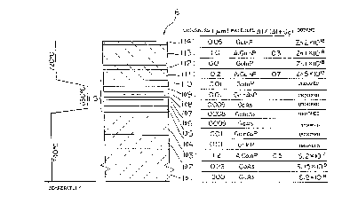
Semiconductor lasers according to a second aspect of
the invention will be described below.
In a semiconductor laser according to a second
embodiment, an epitaxial wafer 116 having a multilayered
structure of Fig. 2 is formed by a reduced pressure MOVPE at
~.'
-- 11 --
~12~
about 60 Torr.
An n-type GaAs buffer layer 102, an n-type AlGaInP
cladding layer 103, a quantum well active layer llS, a p-type
AlGaInP cladding layer lll, a p-type GaInP etching stopper
S layer 112, a p-type AlGaInP cladding layer 113 and a p-type
GaInP cap layer 114 are sequentially formed on a GaAs substrate
101 by epitaxial growth. The quantum well active layer 115
consists of a GaInP cladding layer 104, a GaInAsP optical
confinement layer 105, a GaAs layer 106, a GaInAs quantum well
layer 107, a GaAs layer 108, a GaInAsP optical confinement
layer lO9 and a GaInP cladding layer 110. The p-type AlGaInP
cladding layer 111, p-type GaInP etching stopper layer 112, p-
type AlGaInP cladding layer 113 and p-type GaInP cap layer
constitutes a top clad. The p-type AlGaInP cladding layer 113
is shaped, by subsequent etching, into a protrusion strip that
is coextensive and parallel with a current-injecting portion of
the active layer.
Thicknesses, kinds and concentrations of dopants of the
respective epitaxial layers are indicated in Fig. 2. Also
shown in the left part of Fig. 2 is a variation of the
temperature during the epitaxial growth. It is desired that
AlGaInP for the clads be grown at a higher temperature, and
that GaInAs for the active layer be grown at a lower
temperature. In this embodiment, as shown in Fig. 2, the
active layer 115 is grown at 650~C and the bottom and top clads
are grown at 720-740~C.
~':..".~ '
- 12 -
~1~2319
Then, unnecessary portions of the GaInP cap layer 114
and the ~lGaInP cladding layer 113 of the thus formed epitaxial
wafer 116 are removed by etching. Firs~, a 0.1-~m-thick
silicon nitride film is deposited on the entire surface, and
patterned by a lithography technique to leave a 4-~m-wide band~
like portion 120. Then, the GaInP cap layer 114 and the
AlGaInP cladding layer 113 are etched using the silicon nitride
film 120 as a mask (see Fig. 3). More specifically, first, the
GaInP cap layer 114 and a very surface portion of the AlGaInP
cladding layer 113 are etched out by a mixture at 50~C of
sulfuric acid, hydrogen peroxide and water which are mixed at
a ratio of 3:1:1. Then, the AlGaInP cladding layer 113 is
etched by concentrated sulfuric acid of 60~C until the color of
the wafer surface changes, which means exposure of the GaInP
etching stopper layer 112. Thus, a protrusion strip 121 of the
top clad is formed as shown in Fig. 3.
Then, as shown in Fig. 4, a light diffusion layer 132
of n-type GaInP is formed so as to occupy both sides of the
protrusion strip 121. A GaAs layer 130 and a GaAsP layer 131
are formed prior to the formation of the light diffusion layer
132. As a result of exposure to air, the wafer surface is
rough at the time of restarting growth of the light diffusion
layer 132. In particular, where the surface material includes
two or more group III elements, the surface condition is bad,
i.e., not suitable for the growth of the light-diffusion layer
132. The GaAs layer 130 and the GaAsP layer 131 serve to
_ 13 -
2~L231 9 ~
facilitate the growth of the light diffusion layer 132. The
total thickness of the layers 130 and 131 should be less than
about 50 A, because if they are two thick, they will adversely
affect the optical confinement in the horizontal direction. In
this embodiment, the GaAs layer 130 is 30-A thick and the GaAsP
layer 131 is 10-A thick. The composition of the GaAsP layer
130 need not be selected strictly. At 650~C, the mole ratio
between arsine and phosphine may be set at about 0.1 and the
mole ratio between the group V elements and the group III
element may be set at about 70. The temperature should be
raised in a phosphine atmosphere. Being of an n-type, the
light diffusion layer 132 also serves as a current blocking
layer.
Next, the silicon nitride film 120 is etched out by a
solution of hydrofluoric acid and water (1:1), and a p-type
. ~
GaAs film 140 is formed to have a thickness of 2 ~m. A p-side
electrode 141 is evaporated onto the p-type GaAs film 140.
After the GaAs substrate 101 is thinned to about 100 ~m, an n-
side electrode 142 is evaporated onto it. After the electrodes
141 and 142 are alloyed with the adjacent layers by annealing,
cleaving and mounting steps are performed to complete a
semiconductor laser (see Fig. 5). !
The optical confinement in both of the vertical and
horizontal directions can be controlled by changing the
thickness and composition (distribution) of a base layer of the
top clad, i.e., the AlGaInP cladding layer 111 in this
- 14 -
21~ 2319 ~ ,;
embodiment. Although in this embodiment the mesa shape of the
protrusion strip 121 is an ordinary one (the top is narrower
than the bottom), it may be a reversed one, in which case the
stripe width can be reduced.
Fig. 6 is a top view corresponding to Fig. 5, and shows
how the protrusion strip 121 is arranged on a chip as cut out.
As shown in Fig. 6, ends 121a and 121b of the protrusion strip
121 are separated from facets 152 and 153. The light diffusion
: .: ,- - ,
layer also fills the regions between the end 121a and the facet
152 and between the end 121b and the facet 153 in the same
manner as in the lateral sides of the protrusion strip 121. It
is preferred that distances d between the end 121a and facet
152 and between the end 121b and the facet 153 be about 20 ~m.
Base layers of the top clad, i.e., the p-type AlGaInP cladding
layer 111 and the p-type GaInP etching stopper layer 112 extend
to the facets 152 and 153. Since the above facet structure
causes light diffusion in the vicinity of the facets, the light
density can be reduced there.
A sudden failure may occur in semiconductor lasers
having a GaInAs active layer. The sudden failure is caused by
fusion of a facet, which is called a catastrophic optical
damage (COD) and is considered as originating from an
interaction between light and current at a facet portion. If
the light density is reduced at the facet portions by using the
facet structure of this embodiment, the COD will hardly occur
to improve the reliability of the semiconductor las~r.
21123~9
In this embodiment, the above struc-ture is employed in
both facet portions. Where coatings of different reflectances
are applied to the respective facets, the above structurP may
be employed only for the lower-reflectance-side facet, in which
case the protrusion strip 121 is extended to the facet on the ; ~
higher reflectance side. ;
Fig. 7~shows a multilayered struc-ture of an epitaxial
wafer to be used for producing a semiconductor laser according
to a third embodiment of the invention. The third embodiment -~
is different from the second embodiment in that the light
diffusion layer uses, instead of GaInP, AlGaInP whose
refractive index is larger than AlGaInP of the prot'rusion
strip. To this end, as shown in Fig. 7, the AlGaInP cladding
layers 103 and 113 of the epitaxial wafer 116 of the second
embodiment are replaced by AlGaInP layers 103' and 113' having
a large Al proportion to constitute an epitaxial wafer 116'.
The procedure of forming the epitaxial wafer 116' is basically
the same as in the second embodiment. In the third embodiment,
the temperature in forming the top clad is a little higher than ~ -
in the second embodiment (see Fig. 7). -~
After the formation of the epitaxial wafer 116', a
protrusion strip 121' is formed by etching as shown in Fig. 8,
and then a light diffusion layer 170 is formed as shown in Fig.
9 which is made of n-type AlGaInP having an Al proportion
(Alt(Al + Ga)) of 0.2. Although in this embodiment the light
diffusion layer 170 is formed directly on the etching stopper
- 16 -
21123~9 ~
layer 112, to facilitate the epitaxial growth the GaA~ layer
130 and the GaAsP layer 131 may be formed in advance as ~n the
case of the second embodiment. Then, as in the case of the
second embodiment, the p-type GaAs film 140 and the electrodes
141 and 142 are formed, and a chip is cut out to complete a
semiconductor laser (see Fig. 10).
Figs. 11-13 show epitaxial wafers according to fourth ~ -
to sixth embodiments, which are alternatives to the epitaxial
wafer 116 of Fig. 2. In the fourth embodiment of Fig. 11, an
etching stopper layer of GaAs is employed instead of the
etching stopper layer 112 of GaInP of the second embodiment.
This change provides larger selection ranges to contribute to
stabilization of the manufacturing process. In this
embodiment, for instance, a room temperature solution of
hydrochloric acid, phosphoric acid and water (22~ 17) may be
used as an etchant.
In the fifth embodiment of Fig. 12, an n-side (top)
clad and a p-side (bottom) clad are made approximately
symmetrical. Even in the second embodiment, the light
; 20 distributions on the n and p sides can be made identical by
adjusting the thickness of the AlGaInP cladding layer 111 and
other factors. It is apparent that the epitaxial wafer of the
fifth embodiment can equalize the n-side and p-side light
distributions more easily. ~-
In the sixth embodiment of Fig. 13, the Al proportion
(Al/(Al + Ga)) of a base layer of the top clad is set the same
- 17 -
~"'
:~
21~319
as that of a protrusion strip, to make the large part of the
clad have the same composition. This will facilitate thP
epitaxial growth.
As described above, the semiconductor lasers according
to the second to sixth embodiments exhibit good heat
dissipation performance because they confine light and current
by a structure made of only semiconductor materials. The
single transverse mode operation can easily be obtained by
virtue of the index antiguiding structure. By changing the
thickness and composition of the AlGaInP base layer of the top
clad havin~ an Al proportion smaller than that of AlGaInP of
the protrusion strip, the optical confinement in both of the
.
vertical and horizontal directions can be controlled. ~
:;." ,' . '~,'
'.~
:.', ~:;
- 18 - ~
-. ., '