Note : Les descriptions sont présentées dans la langue officielle dans laquelle elles ont été soumises.
WO 93/01537 PCT/US92/05172
211~57~
-1-
METHOD AND SYSTEM FOR DESIGNING A CUTTING TOOL
The present invention is directed to cutting tools
and, more particularly, to a method for designing a
cutting tool by evaluating predicted tool response and
chip-flow simulations of simulated cutting operations.
The design of cutting tools, and their utilization
in machining materials under various cutting conditions,
has traditionally relied upon a combination of experience
and empirical data. Disadvantageously, this approach is
very time consuming, costly, and difficult to apply.
With the introduction of new cutting tool materials such
as ceramics and cermets, there exisits in the prior art
an even greater demand for chip control, tool reliability
and high performance in view of the complex cutting
conditions under which these new tools are subjected.
In conventional product design cycles, the cutting
tool design engineer usually begins the design of a new
tool with a specific product objective such as: (i)
requirement to cut a specific material, or (ii) utiliza-
tion of a particular cutting speed, feed or depth of cut
in a lathe, mill, or other cutting machine. Based on
previous tool design experience, the designer selects the
tool material which usually consists of a hard substrate
' such as WC-Co with suitable coatings applied to the
surface for further protection against tool wear.
The chipbreaker geometry of the cutting tool surface
is specified based on tool material and machining
.. 30 conditions, and a prototype tool is constructed in
accordance with this geometry and the design
s specifications. Conventional machinability tests for
evaluating the performance of the tool typically consist
of applying the prototype tool insert to the specified
workpiece material over a range of machining conditions
such as cutting speed, depth of cut, and feed rate. As
WO 93/01537 PCT/US92/05172
-2-
the tool insert is applied to the workpiece, chips are
formed with characteristics particular to each cutting
condition. These chips are preferably used to construct
a chip-board matrix depicting the chip geometries as a
function of range of speeds and feeds for a selected
workpiece material. The chip board is then used to
determine the optimal range of cutting conditions for the
newly designed insert based upon chip morphology, chip
microstructure, machine dynamic response (such as
chatter, noise, and power consumption), and wear charac-
teristics of the cutting tool. A desired chip geometry
results when the excess workpiece material is cut into
small, discrete fragments curled substantially in the
shape of the numeral '6'. Long or 'stringy' chips are
considered unacceptable since they reduce the performance
of unmanned machining centers and produce a safety hazard
to machine-tool operators.
Disadvantageously, the prototypical tool design
procedure of the prior art typically does not meet its
desired performance objectives in the first several
iterations of this design and testing process, thereby
causing the designer to repeat the procedure until a
suitable level of performance is attained. This is a
time-consuming process, further delayed by the difficulty
in manufacturing new prototype tool inserts. For
example, prototype cutting tools based on the WC-Co
material mentioned above are manufactured by powder
metallurgy methods but require a complex and expensive
punch-and-die set for cold pressing the powders.
Furthermore, redesign or rework in the tool design or
manufacturing operations lead to further delays and
lead-time in the development of new products.
Another aspect of tool development in the prior art
is the unavailability of results from previous
machinability studies for use in evaluating tool
response. For example, a characteristic of the cutting
WO 93/01537 PCT/US92/05172
21~~~7
- ,
tool industry is that information accumulated by
individual tool designers based on their experience with
diverse machining operations is typically not made
available to the tool industry since the industry lacks a
mechanism for collecting and disseminating such
information. Consequently, there exists in the industry
a need to consolidate the prior information gained in
machinability tests, and to integrate this data into a
system whereby tool design experience can be stored and
easily accessed in a computerized data base.
While the cutting tool industry has historically
designed new tools by repeatedly manufacturing and
testing tool prototypes as discussed above, the prior art
has recently used mathematical models of the
l5metal-cutting process to predict the shear plane angle,
outgoing chip thickness, and forces exerted on the tool
insert. Examples of such predictive models are discussed
by E.M. Trent in Metal Cutting, Butterworths, 1984; M.C.
Shaw in Metal Cutting Principles, MIT Press, 1968; and by
20N.N. Zorev in Metal Cutting Mechanics, Pergamon Press,
1966. Most of these models incorporate an
elastic-plastic material model, but with no temperature
or rate effects included. Good agreement with
experimental results can be achieved with these models
25for the shear plane angle related to the rake angle and
chip thickness. However, these models fail to adequately
describe the process in that they do not account for
friction along the tool-chip interface, strain hardening
of the workpiece, temperature and rate-dependent
30properties of the workpiece, and the mechanics of
separation of the chip from the workpiece. Later
modifications to these models are disclosed by Boothroyd,
et al. in "Effects of Strain Rate and Temperature in
orthogonal metal cutting," J. of Mechanical Eng. Science,
351966 and Stevenson, et al.
WO 93/01537 PCT/US92/05172
_ -4_
As a further modification, Strenkowski and Carroll
in "A finite element model of orthogonal metal cutting,"
ASME Journal of Engineering for Industry (1985) and Usui
in "Progress of predictive theories in metal cutting,"
JSME International Journal (1988) discuss finite element
models of the cutting process. The simulations with
these models occur under orthogonal cutting conditions so
that plane theories of deformation can be applied, and
require machinability data as input (such as chip-shape
and flow lines). However, these models are only
applicable at very low cutting speeds. Additionally,
Benton, et al. in "An adiabatic heating finite element
analysis of metal cutting," MIT (1986), Iwata, et al. in
"Process modeling of orthogonal cutting by the
rigid-plastic finite element method," ASME J. of
Engineering Materials and Technology (1984), and
Strenkowski, supra, illustrate the separation of the chip
from the workpiece by a release of certain nodes in the
finite element mesh as the chip slides across the surface
of the tool. Lee, et al. in "Material modeling and
high-speed machining processes," Advanced Machining
Research Program Annual Report, General Electric Co.,
Schenectady, NY (1982) illustrate the separation by the
'death' of certain elements by removing them from
following iterations of the solution procedure. Analyses
' using rigid-plastic material properties for the chip at
low cutting speeds under isothermal conditions were also
performed as disclosed in Iwata, et al., supra and Lee,
et al., su ra. Iwata's model included a fracture
prediction of the chip from the workpiece, based on the
ductile fracture strain of the steel under consideration.
Strenkowski, su ra, and Strenkowski and Mitchum in
"An improved finite element model of orthogonal metal
cutting," Manufacturing Technology Review-NAMRC XV (1987)
illustrate an updated Lagrangian approach for the inves-
tigation of the cutting process. The material model of
WO 93/01537 PCT/US92/05172
2112575
-
the workpiece was thermo-elasto-plastic with friction at
the interface of the tool and chip. A parting-line
criterion was used for the separation of the chip from
the workpiece, and a critical strain measure was
implemented to determine when the chip would separate.
Large volumes of the workpiece and tool were modeled in
this approach, thus resulting in prohibitively large
computation times.
Benton, et al., supra, abandoned the concept of a
strain-to-failure at the debonding of the chip from the
workpiece in favor of a release criterion based on the
distance of the workpiece from the tip of the cutting
tool.
In summary, the prior art in the design and
selection of cutting tools has lacked an integrated
system for readily accessing machining data and tool
design experience from a database, for comprehensive and
accurate modelling of the physical phenomena in cutting
operations, and for adaptively evaluating tool response
and chip-flow simulations.
Accordingly, the present invention provides a method
of designing a cutting tool based on a simulated cutting
operation characterized by linear and non-linear physical
phenomenon defining the cutting operation of a tool on a
workpiece, comprising the steps of representing said
linear phenomenon with a modifiable linear model which
simulates said linear phenomenon in response to value
assignments for modifiable input parameters, and further
comprising the steps of: representing said non-linear
phenomenon with a modifiable non-linear model which
simulates said non-linear phenomenon in response to value
assignments for modifiable input parameters; exercising
said linear model to derive the simulation of said linear
phenomenon, and exercising said non-linear model to
derive the simulation of said non-linear phenomenon;
_6_
evaluating said simulations with an adaptive judgment
base in a dynamic learning environment; integrating said
simulations and evaluation into said learning
environment; and continuously modifying said input
parameters in accordance with said evaluation until an
acceptable evaluation is achieved.
In the drawings:
FIGURE 1 shows a block diagram of a cutting
tool system in accordance with the present invention;
FIGURES 2A-2C are flow diagrams illustrating
the function of module 12 in Figure 1;
FIGURE 3A shows a schematic of a metal cutting
operation simulated by the present invention;
FIGURE 3B shows a mesh geometry of the tool
nose in Figure 3A;
FIGURE 4 shows an exemplary von Mises stress
distribution in the tool nose of Figure 3A;
FIGURES 5A and 5B graphically depict a
parameter study based on the response shown in Figure 4;
FIGURE 6A shows a debonding finite element in
accordance with the present invention;
FIGURE 6B illustrates modeling of debonding
stress as a function of strain of a finite element
material;
FIGURE 7A illustrates a four-noded bond element
utilized in the present invention;
ycc/fp
a- -.
-6a- 21 12 5 l 5
FIGURE 7B illustrates a stress iso-surface in
accordance with a first debond element of the present
invention;
FIGURE 7C illustrates a stress iso-surface in
accordance with a second debond element of the present
invention;
FIGURE 8 is a stress-strain curve for the
debonding element of Figure 7A;
FIGURE 9 is a photograph of a cross-section of
the chip-forming process showing shear-localized zones;
ycc/fp
WO 93/01537 PCT/US92/05172
2~1~ ~'~
_7_
FIGURES l0A AND lOB show the finite element mesh
geometries used in models simulating non-localized and
localized phenomenon, respectively;
FIGURE 11A illustrates a finite element tool mesh in
accordance with the present invention;
FIGURE 11B shows the 2-D FEA stress results from a
thermally coupled simultaneous analysis of a cutting tool
and metal chip with interface friction;
FIGURE 11C shows geometric modeling of the cutting
surface of a tool;
FIGURE 12A is a side view of an undeformed chip;
FIGURE 12B is a three-dimensional view of a deformed
chip in accordance with the chip-flow simulation of the
present invention;
FIGURE 13 is a temperature distribution of the chip
in Figure 12B;
FIGURE 14 is an amplified view of the chip shown in
Figure 12A, illustrating clearly the location of the
cutting tool and lower surface debonding elements;
FIGURE 15 is a further perspective view of the
cutting operation in Figure 12B;
FIGURE 16 is a perspective view of a deformed chip
in accordance with a simulation of the present invention;
FIGURE 17 illustrates a series of von Mises stress
contours for a deformed chip;
FIGURE 18 shows an overview of the database system
used in the present invention;
FIGURE 19 is a flow diagram used to evaluate a tool
design;
Figures 20 and 21 are schematics of chipbreaker
geometries analyzed by the present invention; and
a, Figures 22 and 23 are chipflow simulations from
cutting operations using the tools of Figures 20 and 21,
respectively.
WO 93/01537 PCT/US92/05172
i '~
,.
-g_
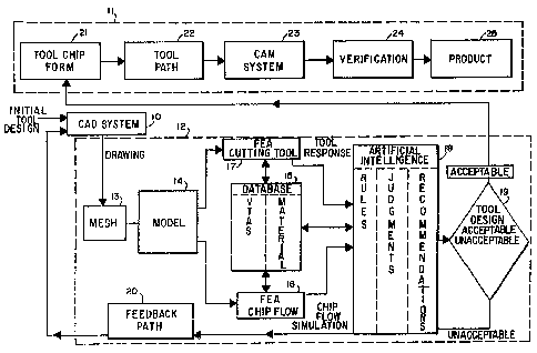
The method for designing a cutting tool in
accordance with the present invention is implemented by
the system shown in block diagram format in Figure 1.
The system includes a CAD (Computer Aided Design) module
10, a manufacturing module ll, and an analysis module 12
for receiving a tool design, predicting the performance
of the tool design in simulated cutting operations, and
manufacturing a prototype tool based on an optimal tool
design from module 12. The following sections detail the
functions and operations performed by each module in
Figure 1, and illustrate the information flow among the
integrated modules.
I. Simulation and Modelinct
The analysis module 12 includes a mesh module 13 for
creating a finite element mesh of a cutting tool
geometry, a model generator 14 for providing mathematical
models based on the mesh geometries, a database 15
including a materials database and a tool cutting
database, a Finite Element Analysis (FEA) Chip-Flow
module 16 for performing a finite element analysis of the
chip formation process, an FEA Cutting Tool Module 17 for
performing a finite element analysis of the cutting tool
response, and an artificial intelligence (AI) module 18
for (i) evaluating the results from modules 16 and 17 by
applying the simulation and response results to a
rule-based comparison hierarchy and by rendering
judgments based on the comparisons, and (ii) proposing a
recommendation for a new tool design embodying
modifications to the models and input parameters. A
decision module 19 reviews the recommendation and awards
control of the system to either feedback module 20 for
further analysis based on the evaluation, or to
manufacturing module 11 to construct a prototype tool
when the tool design is acceptable.
WO 93/01537 PCT/US92/05172
21125' 5 . ..
_9- .,
Figures 2A-2C are flowcharts illustrating the steps
executed by the system in Figure 1 for optimally
designing a tool in accordance with the present
invention. In particular, the flowcharts define the
cooperative interaction between the database 15, the AI
module 18, chip-flow module 16, and tool module 17 in the
system block diagram of Figure 1. Each of the decision
blocks and function statements appearing in Figures 2A-2C
will be described below in greater detail, and will be
identified by a parenthesized step letter.
The particular analysis pursued by the designer is
chosen from among four options: chip, tool, chip and
tool, and three-dimensional (3D). The first three
analyses are two-dimensional and are represented by the
flowchart in Figure 2A, while the three-dimensional
analysis is executed by the steps in Figure 2B. The
steps in Figure 2C are common to all of the analyses.
A. Tool Response
When it is desired to predict only the tool response
during a simulated cutting operation, the flowchart in
Figure 2A executes along branch 30-1. Initially, a tool
geometry is selected with a corresponding set of tool
properties such as stress, strain, and creep. (Steps _a
and b ) .
The simulated cutting operation according to the
present invention is illustrated in the diagrammatic
representation of Figure 3A, and is defined by the
movement of a workpiece 32 along the contact surface of a
chamferred tool nose 31 (with the selected chipbreaker
geometry) of a stationary tool insert 33 held by a steel
o tool holder 34. A chip 35 is formed by removal of
material from the workpiece 32, a physical process which
will hereinafter be referred to as a chip-flow
phenomenon.
WO 93/01537 PCT/US92/05172
2112~'~~
-1O-
Figure 3B is an enlarged view of the tool nose
portion 31 encircled in Figure 3A which represents a mesh
geometry based on the selected tool design. (Step c).
Module 17 primarily utilizes linear finite element
models of the cutting tool nose to investigate the
response of the tool nose to cutting loads, and in
particular has been employed in the design of new
inserts, the test and failure analysis of cutting tools,
and the evaluation of edge preparation methods.
Non-linear responses such as creep (discussed infra) are
also possible in module 17. With respect to the analyses
of particular tool materials, tool behavior is linear for
ceramics, while non-linearities are frequently present in
the tool response of carbides and coated cutting tools.
The tool model is based on the mesh geometry of
Figure 3B, and is constructed from commercially available
linear finite element software packages such as the
software tools GIFTS and ANSYS. (Step d). These software
packages, however, may provide limited non-linear
capabilities, and are executable on personal computer
workstations, thereby facilitating analysis in
laboratories. It should be obvious to those skilled in
the art that other suitable linear FEA packages can be
used, as well as other hardware systems for executing the
code .
' Force vectors representing tool loading due to the
cutting action are indicated by the arrows along the edge
of nose 31 in Figure 3B. These approximate loads are
applied as input parameters to the finite element model
of the cutting tool, and the response of the tool is then
calculated by executing the source code from which the
tool model is constructed. (Step f). One such response
is the predicted von Mises stress distribution throughout
the tool of Figure 3B, which is shown in Figure 4 as a
series of stress contours each with a stress value
WO 93/01537 PCT/US92/05172
~1~2~~5
-11-
alphabetically indexed to corresponding von Mises
criteria in the accompanying legend.
Figure 5A reveals the results of a parameter study
wherein chamfer angle served as an input parameter to the
tool model. The study continually modified chamfer angle
in a series of tool simulations to estimate tool
response, and plotted tensile stress as a function of
chamfer angles to illustrate their interdependence.
Based on this study, subsequent tool life was then
predicted as shown in the bar graph of Figure 5B.
Employing numerically predictive mathematical models to
predict the range of tool responses allows a number of
tool designs to be tested and analyzed without
manufacturing a single physical tool, hence reducing the
number of tool prototypes that have to be manufactured.
The above discussion concerned the steps executed
for predicting tool response. The remaining steps for
displaying results, interpreting/evaluating the results,
and modifying the models and tool designs are explained
below in sections III and IV with reference to the
flowchart of Figure 2C.
When it is desired to include characteristics of the
chip-flow phenomenon as variables for consideration in
the optimal design of a cutting tool, the flowchart of
Figure 2A executes along branch 30-2. The software
package ABAQUS available from Hibbitt, Karlsson, and
Sorenson, Inc. (HKS) of Providence, Rhode Island, is
utilized to implement the models, particularly the
chip-flow model. It will be readily appreciated by those
skilled in the art that the description and requirements
of the chip-flow model as set forth below are sufficient
n to enable one skilled in the art with access to ABAQUS to
write the software code representing the models.
The models discussed hereinafter in accordance with
the present invention were developed using the ABAQUS
Theory and Users Manuals, Version 4.8, copyright 1989
WO 93/01537 PCT/US92/05172
21125'75
-12-
(incorporated herein by reference) available from HKS.
ABAQUS is a batch program which assembles a data deck
containing model data and history data. Model data
define a finite element model with elements, nodes,
element properties, material definitions, and any other
data that specify the particulars of the model. History
data define what happens to the model, and includes the
sequence of events or loadings for which the model's
response is sought. In ABAQUS this history is divided by
the user into a sequence of steps each including a
procedure type such as statis stress analysis or
transient heat transfer analysis.
A finite element model consists of a geometric
description defined by the elements and their nodes, and
a set of properties associated with the elements
describing their attributes such as material definitions
and parameters for interface elements. There may also be
constraints in the model represented by linear or
nonlinear equations involving several of the fundamental
solution variables in the model, and relating to simple
boundary conditions that are to be imposed at the start
of the analysis.
The element library in ABAQUS supports a geometric
modeling capability wherein the elements use numerical
integration to allow complete generality in material
' behavior. Shell and beam element properties may be
defined as general section behaviors, or each
cross-section of the element may be integrated
numerically, so that nonlinear response can be tracked
accurately if desired.
The geometric models according to the present
invention utilize various finite elements of ABAQUS to
simulate certain physical phenomenon, particularly the
chip formation process. For modeling the chip-flow
phenomenon, the stress-displacement element CPE4 is used
when thermal coupling is not represented, while the
WO 93/01537 PCT/US92/05172
2112~7~ . ,,,:: 4
-13-
coupled temperature/displacement element CPE4T is used
when a thermal coupling process is included in the model.
The tool response is modeled by an element (rigid
surface interface element IRS21) which does not
experience defomation, and by two slide line interface
elements ISL21 and ISL21T which allow for tool
deformation during the cutting operation. Element ISL21T
is used when a thermal coupling analysis is desired.
Stree-displacement element B21 is used to model workpiece
rotation, while a user-defined element U1 implements both
debonding finite elements (discussed infra) in a user
subroutine UEL.
The purpose of a finite element analysis is to
predict the response of a model to some form of external
loading, or to some non-equilibrium intiial conditions.
ABAQUS makes available a series of procedures for
facilitating modeling of the particular history to be
analyzed. The ABAQUS history procedures used by the
present invention include *COUPLED TEMPERATURE-
DISPLACEMENT for performing a fully coupled simultaneous
heat transfer and stress analysis, *DYNAMIC EXPLICIT for
performing dynamic stress/displacement analysis using
direct integration, and *STATIC for performing a
non-thermal coupling static stress/displacement analysis.
The above finite elements and response analyses
' should not serve a a limitation of the present invention,
as it should be apparent to those skilled in the art that
other elements and procedures may be used to implement
the tool and chip-flow simulations of the present
invention.
B. Chip-Flow Simulation
Module 16 in Figure 1 simulates the aforementioned
chip-flow phenomenon which is physically represented by
WO 93/01537 PCT/US92/05172
21i257~
-14-
the curling of a metal chip 35 away from a workpiece 32
as shown in Figure 3A. The chip-flow phenomenon is a
non-liner physical process that is not as easily modelled
as the tool response.
The chip-flow phenomenon in metal cutting describes
the mechanics of material removal from the original
workpiece during cutting operations. This phenomenon
inherently involves the formation of new surfaces, large
deformations associated with the creation of chips, and
the internal generation of heat. Possible sources of
such heat generation are sliding contact along the tool
surface and permanent deformation of the chip, although
other sources should be well known to those skilled in
the art. Accordingly, numerical models of the chip-
forming process must accurately account for these
physical processes in order to render accurate
predictions of stress, strain, temperature and other
performance measures. Application of the finite element
method to large deformation problems in solid mechanics
has been documented by Y.J. Bathe in Finite Element
Procedures in Engineering Analysis, Prentice-Hall (1982),
and by O.C. Zienkiewicz in the Finite Element Method,
McGraw-Hill (1982).
There are two principal objectives for modelling the
chip-flow process: (1) calculating the loads and tempera-
tures under steady-state conditions on the surfaces of
the cutting tool to support cutting tool design, and (2)
numerically predicting the chip morphology and
quantifying the stress and strain state to assess the
performance of a given cutting tool material and geometry
on a specific workpiece material.
In practice, the tool is used in a lathe or milling
machine at various speeds and depths of cut.
Observations of the cutting process during machinability
tests, as well as evaluation of the chips that are
created, permit the tool design engineer to describe the
WO 93/01537 PCT/US92/05172
211~~°l
--15 -
cutting conditions under which a tool best performs.
Satisfaction of these two objectives will provide data
for creep and wear predictions of cutting tool inserts
under operating conditions, and greatly reduce the time
and cost needed in the production of improved new cutting
tools.
The following sections describe several physical
mechanisms which exist in the chip-flow phenomenon and
which are represented in the chip-flow model of the
present invention.
With respect to the flowchart of Figure 2A, both the
chip and chip/tool analyses require the selection of
workpiece properties including stress, strain, and
temperature values. (Step g). This exemplary list of
properties should not serve as a limitation of the
present invention, but rather as a representative set of
the workpiece properties well known to those skilled in
the art and selectable by step g.
One novel aspect of the present invention is that
the chip-flow model incorporates a representation of a
fracture mechanism describing a chip separation
phenomenon known as debonding. The chip fracture
mechanism defines a release of said chip from the
workpiece and is represented by a debonding finite
element in the chip-flow model. Consequently,
determining the appropriate debonding properties is part
of the selection of workpiece materials in step q. The
following discussion is a detailed explanation of the
debonding mechanism and its finite element representation
in the chip-flow model.
Debonding
The finite element model embodied in module 16
includes a fracture-mechanics based debonding criterion
for separation of the chip from the workpiece, and time-
.- ° -16-
2112575
dependent and temperature-dependent material properties.
As will be discussed hereinbelow, the model allows for
the use of an explicit time integration scheme for the
equations of motion to permit numerical modeling of the
metal cutting chip flow problem in three dimensions.
More specifically, two debonding elements have been
created to model the separation of the chip from the
workpiece. Both models are fracture-mechanics based
finite elements, and allow time and temperature dependent
material properties. The first debonding element has a
circular stress iso-surface as shown in Figure 7B, while
the second element has a concave-down iso-surface as
shown in Figure 7C. Both elements may be used in metal
cutting simulations where no compression exists along the
chip-workpiece interface (such as in positive rake
cutting). The element with the concave-down iso-furface
is compression.-insensitive and may be used for
simulations where any stress state exists along the
chip-workpiece interface.
First Debondinc Finite ElP~nent (compression-dependent)
The method by which the separation (or debonding) of
the chip from the workpiece is modeled plays an important
role in the morphology and response of the resultant
chip, and temperatures and loads applied to the cutting
tool.
In three-dimensional metal cutting,, the chip sepa-
rates, or debonds, from the workpiece material on two
planes: one normal to the feed direction, and one normal
to the depth-of-cut (DOC) direction. This separation and
creation of new surface was modeled by developing a
fracture mechanics-based debonding finite element 61
which is located between the chip and the workpiece as
shown in Figure 6A.
The debo:.d element provides a mechanism to gradually
release the chip from the workpiece material, and also
WO 93/01537 PCT/US92/05172
.s 211~~)rlJ
.17-
provides a nearly rigid bond for low bond strains. When
a specified bond strain occurs in the neighborhood of the
debonding element, the element begins to fracture.
Fracture here is used in the continuous damage sense,
that is the stresses decrease for increasing bond strain
until zero stress is reached. It remains zero
thereafter; no damage recovery (material healing) is
allowed. The amount of energy dissipated by damaging is
assumed to be equal to the energy required to propagate a
crack across the length of the element. This energy then
serves to heat the chip and workpiece material in
thermally coupled models. The value of this fracture
energy is determined from critical J-integral values for
the workpiece material.
This element 61 debonds when a critical fracture
strain is reached, which is based on the J-integral value
for the workpiece material. The special element has a
damaged elasticity nature with a gradual reduction in
stress-carrying capabilities as the normalized damage to
the material progresses from zero to one. A detailed
explanation of the first debond element follows below.
The element itself consists of four nodes, as shown
in Figure 7A. The element really only provides a bond
between nodes A and B. The material properties of the
workpiece material only have influence over the bond
' between nodes A and B, while nodes C and D are used only
to provide an 'area' for stress calculations. The spokes
illustrated in Figure 7A model the workpiece material.
Previous models of the chip-flow process have not
included such detailed material property-based fracture
of the chip from the workpiece.
This 'area' for stress computations is calculated
from (length * depth), where
length=(1-a) * distance(B,C) + a * distance(B,D) (8)
WO 93/01537 PCT/US92/05172
21i25'~5 w
-18-
and, for plane strain,. unit depth is assumed. The length
is based on the original geometry.
The forces transmitted by the element are simply the
stresses multiplied by length, where the stresses are
computed from the strains. The strain values include
DirectStrain=(VB-VA)/thick and ShearStrain=(UB-UA)/thick
where UB, UA, VB, and VA represent displacements in the
x-direction for node B, the x-direction for node A, the
y-direction for node B, and the y-direction for node A,
respectively.
Since the orientation of the element is fixed, the
forces transmitted between nodes A and B are not truly
direct so that shear forces normal to the chip surface at
node A are not parallel to the Y-axis. In the models of
the present invention, the center of the spokes and the
tool tip both lie on the Y-axis. Advantageously, the
radius of curvature of the unseparated chip is large so
that the approximation errors in the debonding
calculations are very small. The purpose of the element
is to provide automatic debonding as determined by the
cutting process and material properties.
The bond material is based on a damaged J2
plasticity theory. The damage manifests itself in two
forms - a degradation of the yield stress with damage and
a damaged elasticity. Figure 8 illustrates the
stress/strain behavior of the material model. The
material behaves as an elastic material until the
equivalent strain reaches a value of eyd. If the strain
continues to increase monotonically, the damage will
increase from zero when the strain equals eyd to a value
of one when the strain reaches the failure strain of ef.
The equivalent strain is monitored continuously and the
maximum value attained is tracked. The maximum value,
emax' e~als the maximum over all time of ef. The
equivalent strain is calculated as
eeq = (3/2 ei7eiJ)Z, C1)
WO 93/01537 PCT/US92/05172
21127
-19-
where ei~ is the deviatoric part of the total strain ei~.
The material unloads along a damaged elasticity, as shown
in Figure 8.
The damage is calculated from the equivalent strain
as
D = (emax - eyd)/(ef - eyd ( )
) 2
Note that the value of emax must be initialized to
eyd in the following algorithm.
The value for eyd is given by the initial undamaged
yield stress, cry, divided by 2u . The value for a f is
derived from fracture mechanics principles. The energy
required to create a crack of length ~ and width w is
given by JIC*Rw. The strain energy density in the
material is given by the area under the stress strain
curve ( 1/2 c~Ce f) in Figure 8. The work performed
creating new fracture surface must equal the strain
energy dissipated
JIC*~w = 1/2oDefRwt,
where t is the thickness of the element. Solving
Equation (3) for ef gives
ef = 2JIC/crOt (4)
The yield stress of the material continually degrades as
the damage grows:
~yd(D) - (1-D)oC (5)
The material's elastic response is based on a damaged
elasticity. The damaged elastic moduli are given by:
2uD = (1 D)2u (emax/eyd) (6)
KD ( 1 D ) IC ( emax/eyd )
where 2uD and KD are the damaged shear modulus and bulk
modulus, respectively.
The debonding of the material is assumed to
WO 93/01537 PCT/US92/05172
2112~7~ ..
-20-
Second Debondin Finite Element (compression independent)
This element has one node on the chip and three
nodes on the base. The bond is established between the
node on the chip and the center node on the base. The
other two nodes on the base are used to calculate the
effective area associated with the element. The
thickness of the debonding element h is determined by the
user, and is usually some relatively small fraction of
the chip thickness. The geometry of the element is shown
in Figure 7A.
The user must also specify the material properties
of the debonding element. The initial Young's modulus E
0
is usually selected equal to the modulus of the chip
material. Poisson's ratio is assumed to be 0.5. The
maximum failure stress Amax is selected equal to, or, for
softening materials, smaller than the initial yield
stress of the chip material. The critical energy release
rate for full debonding Jc is usually chosen equal to the
critical energy release rate for crack propagation.
Since debonding mainly occurs by shearing the material,
the best choice is probably the release rate for mode II
crack propagation.
The thickness of the debonding element is used to
obtain the debonding strains. The direct strain is
~ - ev/h,
where ev is the relative displacement of the chip normal
to the cutting surface and the shear strain is
eu/h,
where ev is the relative displacement of the chip tangen-
tial to the cutting surface. For small values of the
strains, the direct stress c~ and the shear stress ~ in
the debonding material will be obtained with the elastic
moduli:
= EoE, T = God = 1/3Eo~.
From the direct and the shear stress, we compute an
equivalent stress with the equations
WO 93/01537 PCT/US92/05172
~~12~7~
-21-
a = (a2 + 3T2)1/2 if a > 0
_ (3)1/2 ~T~ if a <_ 0.
Note that the first expression corresponds to the von
Mises stress. Similarly, we define the equivalent strain
s = (E2 + (1/3)712)1/2 if E > 0
_ (3)1/2 ;~~ if E <_ 0.
An equivalent stress iso-surface is shown in Figure 7C.
Once the equivalent stress (strain) exceeds a
critical value a (E ) the material of the debonding
max max
element is assumed to be damaged. The elastic modulus
diminishes with increasing equivalent strain, such that
the equivalent stress decreases linearly with the
equivalent strain. The stress becomes zero once the
equivalent strain reaches the value
Esoft 2Jc/(amaxt)
Hence, we can define a softening modulus
Esoft amax/E soft'
which is the effective modulus for continued loading,
that is further damaging of the material. The
stress-strain law is shown in Figure 8. The amount of
material damage at any given point in time is given by
the damage parameter D which varies from 0 (no damage) to
1 (complete debonding). Hence, D follows from
D = 0 if E <_ a
ma_x
D = (e-~max)/esoft if Emax~~~~max+ESOft
D = 1 if a>~ +e
max soft
For a partially damaged material, the damage parameter
defines a critical damage stress
adam (1 D)amax-(1-(E-~max)/~soft) amax -
(E ~max Esoft)Esoft
and an effective damaged modulus
Edam a/~ (1 (Emax+ESOft)/E) Esoft
The direct and shear stresses follow from
a EdamE' ~ Gdam ~ 1/3 Edam if a>0
a = Eo~~ t - cdam ~ 1/3 Edam if a<_0.
WO 93/01537 PCT/US92/05172
21125'7 5
-22-
If, after damaging, the equivalent strain decreases we
assume that no further damage occurs and hence the
material behaves elastic with Young's modulus Edam (or Eo
in compression) and shear modulus Gdam' If the
equivalent strain increases the damaged modulus changes.
For c~>0 this yields.
dcr = Edamd~ + dEdamE
dT = 1/3(Edamd~ dEdam~)
and for cr <_ 0
dcs = E de
0
dT = 1/3(Edamd~ + dEdam~).
From the previously derived expression for Edam f°llows
_ -2
dEdam ((Emax + Esoft)/~ ~ EsoftdE.
For behavior in tension (o > 0) thus follows
dEdam ((~max + Esoft)/E3~ Esoft(Ed~ + 1/3~d~f)
and for behavior in compression
dEdam - 1/3 ((Emax + ~soft)/E3~ Esoft Esoft~d~.
It is convenient to define the normalized strains
n~ - e/E , n~ _ ( 1/3 )I~/e .
It is also convenient to observe that
~(Emax + ~soft)/E) Esoft Esoft Edam.
After some manipulation this yields for the rate of
change if stress in tension
d~=EdamdE+(Esoft Edam)~nenedE+nEn~d~l]
dT=Gdamd~+(Esoft Edam)~nynEde+n~n~d~)
' and in compression, since nE = 0 and n~ = 1/J3
do = E de
0
dT = Gdamd~+1/3(Esoft Edam)d~=1/3Esoftd~.
The debonding process outlined above for both
debonding elements is modelled with a simple elastic
predictor radial return algorithm. The state variables
are the total deviatoric strains, the damage, and the
maximum equivalent strain. As is well known to those
skilled in the art, the superscripts above variables
WO 93/01537 PCT/US92/05172
~~~~~)rlJ
_.. !. ; ;,' y . :.
-23-
indicate integration. The constitutive calculations
proceed as follows:
1. Calculate the damaged elasticity constants:
2uD (1 Dn)2uemax/e d
Y
KD = (1-Dn)Kemax/eyd
2. Calculate deviatoric and volumetric parts of the
strain rate:
ev = 1/3 dkk
eiJ - di7 _ ev8i
J
3. Integrate the deviatoric strains:
n+1 n
ei~ - ei~ + ateiJ
4. Calculate the new maximum equivalent strain:
en+1 - [3 2 en+1 en+1 Z
eq / iJ iJ l
emax - max(eeql,emax)
5. Calculate trial stress:
Ptr - Pn + At--D. v
Sid - Sid - Sid + At2uDei~
6. Calculate the new damage value
Dn+1 - max(1, (emax eyd)/(ef eyd))
7. Calculate von Mises equivalent trial stress and
radial return f actor:
cs = [ 3/2 Sid Sid l 2
fr = min(1, (1-D)oC/u)
8. Perform radial return on the trial stresses:
Pn+1 - f . ptr
n+1 r tr
Sid - fr. Si.7
The debond element formulation is best described in
two-dimensional form because of its simplicity. It
should be obvious to those skilled in the art that the
above-described debond algorithm is implementable in
Fortran source code which can be used with the ABAQUS
input deck of the chip-flow model to execute the
chip-flow simulation.
WO 93/01537 PCT/US92/05172
~ll~~rr~~~
Thermal Coupling
Another novel aspect of the chip-flow model of the
present invention is that it incorporates a
representation of a heat-generating mechanism describing
a thermal coupling phenomenon. As indicated by step h,
the chip and chip/tool simulations further include the
selection of chip/tool interface properties such as
friction coefficients, thermal properties, and interface
geometries.
The work involved in machining the workpiece and in
causing the material removal process contributes to the
generation of heat. This heat is substantially generated
by three coupled and concurrently operating mechanisms:
permanent deformation of the chip material, fracture of
the chip from the workpiece, and the sliding of the chip
with friction along a contact face of the cutting tool.
It is important to consider this heat generation in the
cutting process because the material properties of the
workpiece and tool material have temperature dependent
properties. This temperature dependency leads to the
characterization of the heat generation as a thermally
coupled phenomenon since the heat generated by the
mechanisms in the cutting process (which depend on tool
and workpiece properties) alter the properties of the
workpiece and tool, which in turn affect the cutting
process.
To properly include this thermal coupling
phenomenon, the chip-flow model of the present invention
incorporates representations of the following phenomenon
and material characteristics: the temperature dependent
. properties of the materials, heat and its subsequent
transfer across the chip-tool interface, and fracture
energy created by the debonding of the chip from the
workpiece.
In particular, the permanent deformation is modeled
by representing in the chip-flow model that a fraction of
WO 93/01537 PCT/US92/05172
_ -.2~ ~-12 5'7 5 : ~~
heat generated by said deformation is introduced into
said deforming chip. The fracture is modeled by
representing in the chip-flow model that a fraction of
heat liberated by said debonding element upon release
from said workpiece is introduced into said chip.
Finally, the chip sliding is modeled by representing in
the chip-flow model that a selected fraction of heat
which is generated by said sliding is introduced into
said chip while the remaining fraction is introduced into
said tool.
As illustrated in Figure 2A, the selection of
chip/tool interface properties is followed by the
selection of a tool and chipbreaker geometry, and also
the selection of tool properties as in step a if a
chip/tool simulation is desired. (Steps h-1). Based on
the chosen geometries, the algorithms of the present
invention generate tool and chip meshes from which
mathematically predictive models of the tool response and
chip-flow process are constructed. (Steps m-o).
However, before proceeding with the simulations, the user
has the option of incorporating a localization mechanism
into the chip-flow model. (Step p).
Localization/Chip Breakage
As introduced above, another novel aspect of the
chip-flow model of the present invention is that it
incorporates a representation of a shear localization
mechanism describing a shearing phenomenon.
Shear localization occurs during the cutting process
when the shear strain of the workpiece material concen-
trates in a narrow band, effectively creating a shear
strain discontinuity in the region of the band. Figure 9
illustrates the size of this zone 91 for specific cutting
conditions on AISI4340 steel. These zones give the chip
a serrated inner surface, and are a precursor to chip
WO 93/01537 PCT/US92/05172
_ 2i125y5v . . _26-
breakage because of the weakened zone and stress concen-
tration at the root of the serrations.
In order to mathematically reconstruct the 'chip-
board' from machinability studies, the model should
predict the onset of chip breakage to correctly estimate
the size of the chips. Inclusion of the localization
process in the chip flow model is therefore a necessity.
Accordingly, the chip-flow model of the present invention
incorporates this physical process by using thermally
coupled material properties, and by including special
finite elements which permit discontinuities in the
strain field.
Most shear localization in metal cutting is due to
thermally-induced negative stress-strain characteristics
of the material; thus, thermally coupled analyses will
permit this phenomenon to occur. In fact, since most
metals strain-harden at a given temperature without the
thermal coupling, shear localization is impossible. When
the localization process begins, the elements in the
primary shear zone undergo very large strains over short
lengths (relative to element size). By using many
elements whose sides and diagonals are approximately
along the direction of localization as in Figure lOB, the
present invention has included this phenomenon in the
model. Figure l0A is shown for comparison purposes to
illustrate how an inappropriate choice of finite elements
will not permit the localization mechanism to be
manifested during the chip formation process.
If the relative size of the shear band becomes very
small, current element technology in cutting simulations
cannot account for the magnitude of the strain jump at
the band. However, it would be obvious to those skilled
in the art that the present invention, and specifically
the localization mechanism, includes other special finite
elements which incorporate displacement (and strain)
discontinuities in their deformation field. Should these
WO 93/01537 PCT/US92/05172
2112~7~ .,
-27-
elements prove useful, they will be included in the
chip-flow model.
In summary, the shear localization mechanism
represents a shear strain discontinuity in a region of
said workpiece and is represented by shear discontinuity
finite elements in said chip-flow model. The
localization mechanism is incorporated into the chip-flow
model by selecting said shear discontinuity finite
elements so as to properly describe said shear
localization mechanism, discretizing said discontinuity
elements, and modifying material property-related
parameters in said chip-flow model to be
temperature-dependent. (Step g).
As presented hereinabove, the chip-flow model
incorporates representations of a fracture mechanism
describing a chip separation phenomenon, a
heat-generating mechanism describing a thermal coupling
phenomenon, and a shear localization mechanism describing
a shearing phenomenon wherein these phenomena occur
during the cutting operation.
The Appendix to the specification is an ABAQUS
instruction set for performing a chip-flow analysis using
the chipbreaker geometries in Figures 20 (design #1) and
21 (design #2). The results of the analyses for the
geometries in Figures 20 and 21 are indicated in the
' chip-flow illustrations of Figures 22 and 23,
respectively. As shown, the primary shear zone 23-1 of
design #2 is larger than the zone 22-1 of design #1,
indicating that design #2 has the better chip control
because the chip is more affected by the chipbreaker
geometry.
C. Chip and Tool Studies
In connection with the discussions above concerning
the phenomenon represented in the chip-flow model of the
present invention, the acquisition of the boundary
WO 93/01537 PCT/US92/05172
~11~5'~5
-28-
conditions on the tool due to the action of the cutting
process is a primary consideration of any chip-flow
model. By describing such boundary conditions, wear and
creep studies based on the simulations can then outline
the performance of the cutting tool. Conventional
models, however, have considered the tool as a rigid
surface which plows through the workpiece material or, at
most, considered only the elastic deformation of the
cutting tool.
Advantageously, the chip-flow models of the present
invention incorporate the strain, rate, and temperature
dependent properties of the tool by way of the thermal
coupling phenomenon (step h), while simultaneously
performing the cutting analysis. Figure 11A shows an
example of a cutting tool finite element mesh according
to the present invention (steps m and n) with high
element density at the tool/chip interface. The
temperatures and loads from the chip flowing by the
cutting tool are transferred to the tool via interface
elements, resulting in the two-dimensional nonlinear
finite element stress results [Pa-von Mises stress] in
Figure 11B computed from a thermally-coupled simultaneous
analysis of the cutting tool and metal chip with
interface friction.
The creep characteristics of the cutting tool are
' such that, in comparison to the rate of flow of the
workpiece material over the tool, no creep of the tool
will be seen over the time period of any chip flow simu-
lation. By suitable modification of the time base of the
cutting tool properties, deformation of the tool can be
observed by simulating the cutting process for a sus-
tained cut.
In addition to simultaneous simulation of the chip-
and-tool, the chip-flow model has implemented accurate
representations of the cutting tool geometry as shown in
Figure 11C. This is a critical part of the chip-flow
WO 93/01537 PCT/US92/05172
-29-
models since the subsequent chip shape and reactions on
the cutting tool are a function of the 'chip-breaker'
geometry (shape of the cutting tool surface).
D. Three-Dimensional Analysis
All prior work in chip-flow modeling has centered
on two-dimensional simulations. Such simulations attempt
to model the 'orthogonal' cutting process in lathe opera-
tions, or other cutting processes where the inclination
angle is zero (such as broaching). Most cutting opera-
tions, however, are three-dimensional in both geometry
and boundary conditions.
The simulations performed in three dimensions
according to the present invention are executed pursuant
to the flowchart of Figure 2B in the same manner as the
two-dimensional chip/tool analysis in Figure 2A, except
that the 3D simulations require 3D geometry and mesh
descriptions (steps w and x), and utilize the ABAQUS
*DYNAMICS procedure (discussed below) including a novel
finite element technique known as an explicit dynamics
formulation for exercising the model. This formulation
is especially suited to problems where large, high speed
deformations occur. The debonding formulation previously
described was included in the three-dimensional model,
but was expanded such that the chip tears away from two
' surfaces of the workpiece material, rather than one as in
the two dimension cutting simulations.
Figure 12B illustrates the three-dimensional nature
of the cutting process with a non-zero inclination angle,
while Figure 13 illustrates the 3D temperature gradients
in the chip. It is expected that the tool designer will
use such a three-dimensional simulation when it is felt
that two-dimensional analyses are insufficient, such as
at the end of the design cycle.
WO 93/01537 PCT/US92/05172
211~~~15 -30-
Explicit Dynamics Time Integration
The equations of motion for the chip-flow problems
are
0*T - pu + pfg = 0, (g)
where p is the mass density per unit volume, a is the
acceleration of the material point, and fB is a specific
(force per mass) body force vector, T is the true stress
in the deformed configuration.
We seek the solution to Equation (9) subject to the
boundary conditions
a = f(t) on Su, (10)
where Su represents the portion of the boundary on which
kinematic quantities are specified (displacement,
velocity, and acceleration). In addition to satisfying
the kinematic boundary conditions given by Equation (10),
we must satisfy the traction boundary conditions
T*n = s(t) on ST, (11)
where ST represents the portion of the boundary on which
tractions are specified. The boundary of the body is
given by the union of Su and ST, and we note that for a
valid mechanics problem, Su and St have a null
intersection.
The jump conditions at all contact discontinuities
must satisfy the relation
(T+ + T )*n = 0 on Sc, (12)
where Sc represents the contact intersection, and the
superscripts "+" and "-" denote different sides of the
contact surface.
The Lagrangian form of the continuity equation is
written as
p - ptrD = 0. (13)
This is satisfied trivially in our formulation since we
do not allow mass transport. Equation (13) degenerates
to
pV = pOVO, (14)
WO 93/01537 PCT/US92/05172
21I257~
-31-
where V is the volume, and the subscript "0" denotes a
reference configuration.
The conservation of energy principle equates the
increase in internal energy per unit volume to the rate
at which work is being done by the stresses plus the rate
at which heat is being added. In the absence of heat
conduction.
E~ p ( A Em/A t ) - cs : d+ F S2 ( 15 )
where Ev is the energy per unit volume, Em is the energy
per unit mass, and Q is the heat rate per unit mass, c~
the stress, and d the strain rate.
ABAQUS uses a modified central difference scheme to
integrate the equations of motion through time. By this
we mean that the velocities are integrated with a forward
difference, while the displacements are integrated with a
backward difference. The integration scheme for a node
is expressed as
EXT INT
ut = (f t - f t )/M (16)
iit+et = iit + Atiit ( 17 )
ut+At - ut + ~tiit+~t (18)
where fEtT and fltT are the external and internal nodal
forces, respectively, M is the nodal point lumped mass,
and ~t is the time increment.
The central difference operator is conditionally
stable. It can be shown that the stability limit for the
operator with no damping is given in terms of the highest
eigenvalue in the system (Wmax)'
At <- 2/wmax (19)
Equations (9) through (18) were discretized in the
usual finite element manner for 8-noded hexahedron
elements. A complete description of this process is
provided by Taylor et al. in "Pronto 3D-A
Three-Dimensional Transient Solid Dynamics Program,"
SANDIA report SAND87-1912, V6-32 (March 1989).
WO 93/01537 PCT/US92/05172
-32-
E. Cutting Simulation
A tool study was performed in accordance with the
present invention by simulating the cutting of an AISI
4340 steel workpiece with two different hardening rates,
while other cutting parameters (depth of cut, speed,
feed, and tool orientation) were held constant.
The following cutting conditions were used:
Cutting tool:TiC-coated WC-Co flat tool
without chip breaker.
~ Coulomb coefficient of friction, u=0.10
Rake angle = 10°
Inclination angle = 10°
Cutting speed = 1.75 m/s
Feed = 0.127 cm.
The AISI 4340 material properties are as follows:
Shear modulus, 2u = 150 X lOgPa
Bulk modulus, K = 196.1 X lO9Pa (v = 0.33)
Initial Yield, ~0 = 800 X 106Pa
Hardening modulus, H = 500 X 106Pa and 100 X
10 3Pa
Initial temperature, TO = 0 K
Stress intensity factor, JIC = 87600 Nm/m1~5
Thickness of bond material layer, t = 0.5 mm
Adiabatic factor, 1/pcv = 2.618*10 7 m3/J-K
~ ef = 0.438 [from Equation (4)]
' ~ Plastic work heat fraction, Wp = 1.0
The mesh of the uncut workpiece is shown in Figure
12A. The mesh contained 2048 8-noded solid elements and
832 debonding elements containing a total of 3980 nodes.
The cutting simulation was run for 15.0 us, enough time
to allow substantial curling of the chip over the rake
face of the tool. Solution data (stress components,
strains, strain rates, invariants, temperatures, etc.)
was written to disk every 0.25 us, so that 60 "snapshots"
35of deformation were recorded, permitting animation of the
WO 93/01537 PCT/US92/05172
- 2112 5'7 ~ s
-33-
time-dependent solution variables. Computation time for
the three-dimensional simulation was 32 cpu hours on a
VAX 8800. This means that depending on the number of
other processors currently running, the simulation
turn-around could vary from 2 days to 1 week (wall-clock
time) on a machine of equivalent capabilities.
The first simulation with hardening rate of 500E6 Pa
simulated 4340 steel, while the second was a nearly
elasto-plastic material which could be thought of as a
104340 steel at elevated temperatures. Figures 12A and 14
show the mesh of the chip at t=0 s, illustrating the tool
orientation and position of the debonding elements. Note
the rake and the inclination angles of 10°.
During the three-dimensional cutting simulation,
l5many time-dependent parameters were calculated at every
node and gauss point in the mesh for every iteration
during the solution process. These parameters include
deformation, strain, strain rate, stress, principal
stresses and strains, von Mises, tresca, and hydrostatic
20components, temperatures, plastic strain, and actively
yielding flags.
Results are presented for the H - SOOE6 Pa case
first, followed by the H = 100E-3 Pa case. Figure 15
illustrates the deformation of the chip at an
25intermediate time step in the solution procedure, with
' the chip being in thermal and mechanical equilibrium.
Note the curling of the chip in several directions,
opposed to the single radius of curvature found by
similar two-dimensional models. Heat is generated in the
30modeis by fracturing of the chip from the workpiece,
friction along the tool-chip interface, and by plastic
deformation of the workpiece material. This heat
generation was fully discussed hereinabove in connection
with the thermal coupling phenomenon. We have assigned
35x11 of this work to the generation of heat in the chip
volume, although other assignments are possible within
WO 93/01537 PCT/US92/05172
21125"5:
-34-
the scope of the invention. Other researchers have
concluded that little heat is transferred into the uncut
material of the workpiece, substantiating this
assumption. The temperature distribution in the chip
would be reduced when conduction into the cutting tool
convection and radiation terms are fully modeled.
Furthermore, a more accurate temperature-dependent
material model for the workpiece would further reduce the
maximum chip temperature.
The deformed shape at an intermediate time interval
for the H=100E-3 Pa case (Figure 16) shows the change in
chip shape for a lower hardening rate material. Note the
increased contact zone in these figures, compared to the
case with the larger hardening rate. Figure 17
illustrates the distribution of the von Mises stress in
the deformed chip at this time interval of the solution.
The successful simulation of the chip-flow process
in three-dimensions facilitates an analysis of metal flow
over the tool face. Three-dimensional simulations
clearly give much more information about the morphology
of the chip in its deformed state. Chip curl radii in
several directions can be easily resolved from the images
of the deformed shapes, or directly from the solution
data. This information is useful in the "numerical
construction" of chips-boards to judge the application
range for a given tool and workpiece geometry. The
higher hardening rate material provides a tighter chip
radius since the stress state through the thickness of
the chip is much less uniform, resulting in a tendency to
curl the chip .
The tighter chip curl radius also results in a lower
contact area (patch) for the H = 500E6 Pa case. This
could conceivably reduce wear and heat transfer in the
rake face of the chip, depending upon the reaction forces
and temperatures in the contact zone. This information
on the contact region is also indicative of how cutting
WO 93/01537 PCT/US92/05172
2~1~5"~~.
-35-
tool edge geometry will effect the morphology of the
chip. For instance, small t-landed edge designs will
have little effect on resulting chip shape for
elasto-plastic materials.
The curling of the chip in several directions can
provide a means to investigate the breakage of the chip
from the workpiece. For example, if the chip curls in a
manner such that it hits the just-machined surface of the
workpiece, or curls back and hits the tool holder, the
force encountered during this impact is usually
sufficient to break the chip away. This is frequently
seen in the machining of steel workpiece materials. In
order to predict chip lengths from models, bending
moments could be applied to curled chips of various
lengths to determine the final chip size.
The highest temperatures encountered in the chip
occur at the intersection of the planes containing the
debonding element. This has been demonstrated in
infrared temperature measurements of the cutting process.
In the numerical model, this temperature peak in the chip
occurs because the energy released in fracturing the chip
all goes into the creation of heat energy, and also
because this is a corner of the chip, so the heat
transfer rate is smaller than if this heat source was
251ocated at the center of the chip volume.
Several enhancements can be made in the model prior
to use in a tool-design environment. These include a
more accurate material model for the workpiece, which
would require temperature and strain-dependent material
30properties, and temperature-dependent fracture toughness
for the debonding element. Also, specific cutting tool
chip breaker geometries could be used as input for the
analyses. Lastly, improvements in computer speed and
visualization would be required for improved post
35processing of the large data sets created during a
three-dimensional simulation of the cutting process.
WO 93/01537 PGT/US92/05172
-36-
The above results demonstrate the possibility of
using three-dimensional cutting simulations to support
cutting tool design. In fact, the computational time to
complete the three-dimensional chip-flow analysis is
manageable with a minisupercomputer, thus making this a
viable method of analyzing the chip formation process for
turning and milling operations.
The linear finite element analysis of the present
invention has been applied to the design of a ceramic
chipbreaker disclosed in U.S. Patent No. 4,963,061.
II. Artificial Intelligence
Once the mathematical models have been exercised to
provide predictive performance results of the tool
response and chip-flow simulation, the results are
reviewed by an artificial intelligence (AI) module 18 in
Figure 1. (Steps aa-gg in Figure 2C).
In accordance with the present invention, each
simulation model can be represented, for illustrative
purposes only, by a function y=f(x) wherein x is an input
vector of modifiable parameters, and f(x) is the series
of mathematical relationships between the input x and
output vector y. In the present invention, f(x) will be
an implicit function of the design variables x, since a
25suitable chip-flow analysis using ABAQUS is necessary to
find the function f for a given set of x.
The AI system includes a hierarchical structure of
rules for comparing the predicted y vector to
predetermined acceptability criteria y'. (Step ee). This
30rule-based comparison produces a judgment which indicates
whether the predicted response is acceptable or
unacceptable within the constraints of the rule. (Step
ff ) .
Based on these judgments, a recommendation is made
35to modify the defining relationships of the model
represented by f(x) and/or modify the parameters of the
WO 93/01537 PCT/US92/05172
~11~5r1~
-37-
input vector x. (Step qq). Specifically, the new design
parameters of the chip-flow and tool models are returned
to the mesh and model-generating steps m, n, and w for
constructing new models to be exercised. (Step ii).
Thus, it is apparent that the AI system performs a
rule-based comparison module, renders judgments based on
the comparison, provides a recommendation embodying said
judgment, and modifies the model/input parameters in
accordance with the recommendation.
Figure 19 illustrates the decision-making process
involved in a rule-based system for evaluating the design
of a cutting tool, and is representative of the logic
flow of the AI module 18 for tool response and chip-flow
simulations. The tool design is characterized by
l5parameters such as land-width, land-angle, chip-breaker
depth, form-width, incident-angle, and other variables
relating to the geometry and angles of a chip-breaker
design on the cutting nose of the tool insert. These
listed measures are only a representative list as it
should be well known to those skilled in the art that
other measures are also included.
As indicated in Figure 19, these variables are
applied to rule-based decision blocks embodying tool
requirements relating to such evaluative measurements as
25geometric characteristics, stress, and temperature
levels. Based on the acceptability of these
measurements, the design variables are appropriately
modified until an acceptable design is achieved.
In accordance with Figure 19, an AI module for
30evaluating tool and chip-flow simulations would use
characteristics such as chip size, chip radii, chip
thickness, localization, and other such parameters
available from chip-board matrices to evaluate the
simulations. In particular, a design vector of the
35above-identified variables is used to design a tool such
WO 93/01537 PCT/US92/05172
~11~5'~~',:
-38-
that tool failure does not occur and suitable
chip-control is obtained.
In order to implement AI module 18, a set of
pre-existing rules on the strength of the tool material,
and acceptable sizes and shapes of the resultang chips
would be stored within the cutting tool data base. At
every tool design iteration (i.e., after a chip-flow or
cutting tool analysis), the chip size and stresses within
the cutting tool would be compared to the values in the
database. Any conditions that are violated will
necessitate computation of the appropriate changes in the
design variables such that the rule-based judgments in
subsequent iterations will converge to an acceptable
design.
As discussed above, and outlined in the instruction
sets of the Appendix, the present invention provides as
an input deck to ABAQUS a description of the chipbreaker
geometry and boundary conditions; node coordinate
specifications; element definitions for chip, spokes,
bonds, and tool-chip interfaces; stress-strain curve
data; material property definitions; and analysis type.
It should be apparent to those skilled in the art that
modifications can be made to the instruction sets to
supplement the analysis with other ABAQUS subroutines.
Once analysis results are produced, the simulation
is evaluated. For example, in the drawings of Figures 22
and 23, the degree of localization in the primary shear
zone is used to compare the relative merits of designs #1
and #2. If the analysis is modified to allow for chip
removal, data available from chip-board matrices, such as
chip size, radii, and thickness, is used to evaluate chip
control.
Although the analysis for designs #1 and #2 differ
only in the chip-breaker geometries being analyzed, the
representative set of parameters for the input deck
listed above can be modified on subsequent iterations.
CA 02112575 2000-09-14
-39-
However, if such parameters are fixed to correspond to a desired
cutting environment, the chipbreaker geometry is changed by
modifying the interface element definition until an acceptable
chip-flow simulation i.s achieved. Other analyses which a
designer may review in conducting the simulations include
temperature distr~_buti.ons, reaction forces on the contact
surfaces, and stre:~s-strain levels.
In the present invention, the knowledge base for the
expert system is derived from the material and VTAS database
from all previous tool trials. The inference engine is a
program which controls the testing of internal rules, or "IF-
THEN" statements 'which make judgments on the current tool
design.
While each programmable function and operation executed
by the algorithms of the present invention consists of one or
more equations embodied in a numerical model, the invention is
not so limited to m«delS wlth specific relationships between the
input and output v~~riabl~=s .
In certain applications to be represented by an expert
system, the :required relationship between variables may be too
complex to be represented by an equation. In such cases, it may
be necessary to extrapolate the desired result from available
data. One way to accomplish this extrapolation function is by
including a neural-net in. the system model section of the expert
system architecture of t:he present invention. A neural-net is
a software simulavion of a parallel distributed processing
system in which each node is similar to a neuron and connected
to all other nodes. In
WO 93/01537 PCT/US92/05172
-40-
typical applications as known in the art, neural-nets are
used either for pattern association, where a set of
patterns are associated with another set of patterns, or
for auto-association, where a partial input pattern is
associated with its complete pattern. In applying
neural-nets to the present invention architecture, the
neural-net is utilized to associate a set of input data
with a set of output data. The data module provides the
user with an input and an output file. Using these
lOfiles, the user enters into the system a set of input and
output data. The data module then calls the neural-net
software and passes to it the information contained in
these files. Using this data, the neural-net software
learns the relationship between the input and output
data. This relationship is stored in the neural-net as
weights, or strength of connections, between input and
output nodes representative of the input and output
variables. Subsequently, the data module asks the user
for a set of new input parameters. The data module then
passes the new input data to the neural-net. Using the
weights between input and output nodes, the neural-net
software determines the output data associated with the
input data submitted by the user. Thus, the operating
flexibility of the expert system can be enhanced by use
25of neural-net technology. A brief description of
performance of pattern association by neural-nets is
provided in the reference entitled "Parallel Distributed
Processing" by Rumelhart, et al., Vol. 1, page 446, the
MIT Press, Cambridge, MA.
While in accordance with the architecture of the
preferred embodiment of the present invention the various
software functions performed within the system architec-
ture are each designated as part of one of the architec-
ture modules, the invention is not so limited. As will
35be recognized by those skilled in the art, the
designations of program and data modules as well as the
WO 93/01537 PCT/US92/05172
.. 2i125'~5
-41-
other architectural components, while preferred herein,
are primarily for convenience in organizing the various
program functions. To some extent, the various functions
could be allocated differently among the architectural
modules or, alternatively, different modules could be
designated and program functions assigned thereto, all
without affecting expert system operation.
III. Database Creation
The database module shown in Figure 1 interacts with
the simulation modules 16 and 17 of both the chip-flow
and tool responses, respectively, and with the AI module
18 in rendering new tool designs.
Presently, the database implemented in the system of
Figure 1 is the Valenite Tooling and Analysis Software
(VTAS) package available from GTE Valenite Corporation of
Troy, Michigan. VTAS receives basic information from a
user about the cutting application, such as speeds,
feeds, and materials, and executes algorithms to match
20the characteristics of the cutting operation to the best
choice in tool grade and geometry. This method has the
advantage of being able to extrapolate information from a
limited amount of internal and external data to make
useful recommendations on almost any cutting operation.
VTAS combines a materials database with a cutting
database as shown in Figure 18. The following list of
database parameters should not serve as a complete
recitation of the data values available to the analysis
module 12, but rather as an exemplary subset of
30parameters whereby other parameters should be readily
appreciated by those skilled in the art to be included in
the present invention.
The cutting database includes empirically determined
information about the cutting condition and machining
35parameters. The cutting condition includes data on such
parameters as cutting speed, feed, and depth of cut,
CA 02112575 2000-09-14
-42-
while the machining parameters include data on static and
dynamic factors, operational features (turning, milling,
drilling, thread cutting), and thermal effects. Parameters such
as forces and tempE~ratures are acquired by equipment well known
in the art for monitoring cutting operations, such as the ISAAC
5000 Data Acquisition system, infrared sensors, and the
Dynametrics measurement assembly.
The materials database includes primary physical and
mechanical properties of the tool and workpiece. For example,
cutting tool parameters include tool geometries, chip form
(chipbreaker designs and constraints), bit grade, deflection
shoulders, loadabiLities, working ranges, and suitability for
different workpiece materials, cutting conditions, stabilities,
cutting rates, chid cro~;s-sections, and individual processing
methods. Workpiece pro~oerties include treatment conditions,
hardness, alloying components, mechanical strength, surface
conditions, machining behavior, and raw and finished dimensions.
The material properties and cutting conditions together
provide the boundary conditions of the cutting operation.
The VTAS database is continually modified as new
workpiece mat.eria~_s, tool inserts and tool materials are
studied. Similarl~r, when some contents of the database become
obsolete, they will be removed from the database. Also,
simulation results are included in the database, and can be
easily modified when ne:w models which describe the cutting
process are derived. Th.e results from the simulation studies
which are to be included into the machinability database do not
include any experimentally-determined variables (such as chip
thickness) in the analysis. This means that only primary
physical and
WO 93/01537
2112 5 ~~ ~ PCT/LJS92/05172
-43-
mechanical properties of the tool and the workpiece (such
as stiffness, thermal conductivity, and yield strength)
are used to simulate machine tests. This analysis is
supplemented by database information on forces and
temperatures of the cutting operation, which are measured
from actual cutting operations.
It should be obvious to those skilled in the art
that a computer-accessible and modifiable database other
than VTAS is implementable in a computer system and
therefore forms a part of the present invention, wherein
such a database combines machining data, materials data,
cutting operation information, and results of simulated
and real-time tool studies.
IV. Animation/Results Evaluation
Chip-flow modeling generates very large data sets,
since all parameters (temperature, stresses, strains,
invariants) are monitored for every increment in the
simulation. Such large volumes of information require
20novel visualization techniques for interpretation of the
data. Previous work has centered on contour plots (still
images), or frame-by-frame animation of the incremental
data. GTE Laboratories Incorporated of Waltham,
Massachusetts, has produced an animation system which
25allows the tool designer to interact with the data set as
it is being visually represented. Currently, the
deformation and a single time-dependent parameter (such
as temperature) may be monitored during the animation.
The animation tools, however, are modifiable to permit
30the simultaneous rendering of several time-dependent
parameters.
V. Manufacturing of Tool
Once the decision module 19 in Figure 1 determines
35that the tool design is acceptable, system control is
awarded to the manufacturing module 11 for fabricating a
WO 93/01537 PCT/US92/05172
_ 211 ~ 5 ~l 5 -44-
physical tool prototype as discussed in section A. below,
or for fabricating a plastic tool prototype as discussed
in section B. below. (Step hh in Figure 2C).
A. CAD-CAM Integration
A computer-aided design (CAD) module 10 in Figure 1
is employed by GTE Valenite Corporation of Troy,
Michigan, in generating tool prototypes based on
acceptable tool designs using a Unigraphics workstation
to produce three-dimensional tool geometries which are
directly downloaded to a chip form module 21. Module 21
preferably includes a 4-axis mill for cutting a tool form
with the desired chipbreaker design.
A computer-aided manufacturing (CAM) module 23
receives the tool form and produces a physical cutting
tool. However, the fabrication of a physical tool
prototype with a conventional CAD/CAM system possesses
the following disadvantages:
Inability to incorporate, enhance, and
manufacture more sophisticated design elements
in chipbreaker geometries.
Difficulty in transferring accurate dimensional
design details into manufacturing.
Time restraints on receipt of engineering prints
and hard tooling.
~ Additional manufacturing time needed to
incorporate improved design changes.
Accuracy/repeatability of ground prototypes.
Performance changes are not easily implemented
from ground prototype to final pressed product.
~ Transfer of dimensional design requirements on
additional styles.
Manufacturing time needed to produce test pieces.
CA 02112575 2000-09-14
-45-
B. Plastic Toolincr
The present invention preferably utilizes the
conventional CAD/C'AM assembly discussed above with a novel
process employing plastic as a die material for producing
plastic tool prototype:>. The plastic tooling process is
directed to a method for making a compact for a densified
cutting insert of a hard refractory material having a
predetermined desired shape, comprising the following steps: (i)
forming a machinable wax material into the predetermined desired
shape, (ii) contacting t:he shaped machinable wax material with
an uncured flowable liquid moldable plastic material and curing
the moldable plastic material to form a substantially
incompressible solid plastic mold, and (iii) compacting a
powdered mixture comprising an organic binder and hard
refractory particles into contact with the mold at a sufficient
pressure to form <~ compact having the predetermined desired
shape.
The advantages of a CAD/CAM system implementing plastic
tooling include the following:
~ Abilivy to incorporate, enhance, and manufacture
more :~ophisl=icated design elements in chip-breaker
geometries.
~ Produce 3-D models of required chipbreaker designs
via a CAD system.
~ Produce machining coordinates via CAD/CAM link to
4-axi;~ milling machine to produce press tooling.
~ Subst<~ntial time savings for improved design
changes.
WO 93/01537 PCT/US92/05172
21~2~7~
_ -46-
Repeatability/accuracy of each chipbreaker design
is machine tested.
Accurate Translations of required chipbreaker
design into manufacturing.
~ Improved manufacturing times on engineering
drawings and hard tooling.
Complete design requirements on additional styles
before producing hard tooling sets.
Quick response for capturing smaller mark
windows.
Taking designs risks without high up-front costs.
The plastic tooling of prototypes in combination
with the optimal designing of cutting tools by performing
simulations of various cutting operations offer tool
designers significant savings in development time and
engineering resources.
Advantageously, CAD/CAM plastic tooling in
accordance with the present invention has been employed
in light duty tool standards development and
customer-requested special deliveries, and has potential
uses in the actual manufacture of tool inserts.
IV. EXTENSIONS
This invention greatly reduces the time required to
design and select cutting tools by virtually eliminating
the trial and error process currently used, and replaces
it with an integrated CAD/CAM, machinability database
that has retrievable information from all previous
machinability studies performed, on-going machinability
studies, and the results from simulating the chip-flow
process by detailed numerical models of the material
removal process. The key element is the integration of
the database with the CAD, CAM and numerical simulations,
tailored specifically for cutting tool manufacturing
(Figure 1).
WO 93/01537
21125'~~
-47-
PCT/US92/05172
It should be readily appreciated by those skilled in
the art that such a system as described herein can serve
as a manufacturing cell responsive to customer requests
for providing either a tool design or a plastic tool
prototype based on this design. In particular, a
customer's request may include a description of the
desired tool materials, workpiece, and cutting
environment from which the simulated machinability
studies of the present invention can provide a range of
tool designs with associated performance measures for
review and selection by the customer. Once an optimal
design is chosen pursuant to the customer's special
requirements, a plastic tool prototype can be
manufactured, or preferably a set of prototypes with
different designs are manufactured for testing and
evaluation since the plastic tooling process affords such
batch production in a short period of time.
The following is a summary of the modules in the
cutting tool system of the present invention along with
the benefits and opportunities available with each such
module.
CAD CAM
~ Increase manufacturing efficiency on special
short run jobs.
~ Reduction in time/manpower/cost by utilizing
plastic tooling.
DATABASE
~ Real-time process control.
~ On-demand benchmarking information.
TIME-SHARING
~ Common FEA resource for engineering applications.
~ Capability for modeling of complex problems such
as milling and drilling.
~ Linkage of material/tool/toolholder models.
WO 93/01537 PCT/US92/05172
-48-
SUPER-COMPUTING NETWORK
Improving speed of ABAQUS calculations.
CHIP-BREAKER DESIGN
Short term tool optimization on specific job
applications.
Field accessible resource for problem solving.
FAILURE ANALYSIS
Performance predictions based on physical property
measurement.
~ "Expert system" based grade selection.
Product analysis in terms of manufacturing
tolerances.
While preferred embodiments have been illustrated
and described herein, it will be obvious that numerous
modifications, changes, variations, substitutions and
equivalents, in whole or in part, will now occur to those
skilled in the art without departing from the spirit and
scope contemplated by the invention. Accordingly, it is
intended that the invention herein be limited only by the
scope of the appended claims.
30
90-3-850
WO 93/01537 PCT/US92/05172
211'z5~1
-49-
APPE~II~ TO SPECIFICATION
PACE 1 of 26
*HEADING, LTNSYMHi
RATE IHmEP, 10 DEGREE RAKE (FROM VERTICAL)
SPEED - 1.75 M/S, FRICTION=0.5, GRADED MESH
DEBONDING ~~1T
**WAVEFRONT MINIMIZATION, SUPPRESS
** put restart at a freq. of 1000 to write only LAST iteration
*RESTART, WRITE, FREQ=1000
**
** NODES
**
*NODE, SYSTE~i=C
1, 0.10033, 90.000
1001, 0.10033, 90.000
9001, 0.10160, 89.945
*NSET, NSET~BL
1001
*NSET, NSE't~TI~
9001
*NFILL, BIAS-0.8, NSET=LHS
BL, TL, 8, 1000
*NSET, NSET-L&S, GEN
1, 9001, 1000
*NCOPY, OLD SET=LHS, CHANGE NUMBER=1, SHIFT, MULTIPLE=64, NEW SET=ALL
0., 0., 0.
0., 0., 0., 0., 0., -1., 0.159
*NSET, NSET=ALL
LHS
*NSET, NSET-BOT, GEN
1001, 1065, 1
*NODE, NSET-MASTER
50001, 0., 0.
*NCOPY, OLD SET-MASTER, CHANGE NIJI~ER=l, SHIFT, MULTIPLE=64
0., 0., 0.
0., 0., 0., 0., 0., -1., 0.0
*NSET, NSET=CEHTER, GEN
50001, 50065, 1
*NODE, NSET-TOOL
60000, 0.0, 0.10033
**
* * DEFINE ELB~TTS
**
** CHIP
**
*ELEM~NT, TYPE=CPE4
1001. 1001, 1002, 2002, 2001
C~' ( i'~ I1.YITf tT~ f~! t ~"P'~P
WO 93/01537 PCT/US92/05172
~~.~.~~7~ -so-
APPEI~IX ~ SPECIfICATI~d
PACE 2 of 26
*ELGEN, ELSET=CHIP
1001, 64, 1, l, 8. 1000, 1000
*SOLID SECTION, ELSET=CHIP, MAT=ST4340
*MATERIAL,.NAME=ST4340
*ELASTIC
209.OE9, 0.33
*PLASTIC
** this is the "CHIPB" stress - strain curve
800.OE6, 0.00
850.OE6, 0.10
800.OE6, 0.25
750.OE6, 0.50
700.OE6, 1.00
700.OE6, 1.25
700.OE6, 1.50
700.OE6, 2.00
***RATE DEPENDENT
** 40.0, 5.0
*SPECIFIC HEAT
**J/kg -R
599.13
*DENSITY
**kg/m**3
7700.0
*CONDUCTIVITY
**~,7~-R
43.0
***EgPANSION
** ~
**21.6E-6
*INELASTIC HEAT FRACTION
1.0
**
** SPORES
**
*~~1T, TYPE-B21, ELSET-SPORE
50001, 50001, 1
*ELGEN, ELSET-SPORE
50001, 65, l, 1
*BEAM SECTION, MAT-SPORE, ELSET=SPORE, SECT=RECT
** WIDTH, DEPTH
1.0, 0.1
*j~,TF.RTAT.~ $pO~
*ELASTIC
209.OE9, 0.33
**
** BONDS
**
*USER ELEMENT, TYPE=U1, NODES=4, COORDINATES=2, PROP=7, VAR=2, UNSYMM
1. 2
*UEL PROPERTY, ELSET=BOND
** E1. E2, EP1, EP2, EZ1, EZ2, THICK
** WHERE THICK*EZ1 = 2*J1C/SIGY1, THICK*EZ2 = 2*J2C/SIGY2
** AND SIGY2 ~ SIGY1/2 AND E2 = E1/(2*(1+NU))
** J1C = J2C = 87600 N-M/M**2 (= 500 IN-LBF/IN**2)
200.OE9, 75.2E9, 4.OE-3, 3.33E-3, 3.6~, 'x.30, 0.06E-3
~~~Pa~.s~rsR~ w,.sa s.~ess,p
WO 93/01537 PCT/US92/05172
21125'
-
APPE1~II?: TO SPECIFICATIC~1
PAGE 3 of 26
*ELB~''NT. TYPE-U1, ELSET-BOND
1, 1, 1001, 10.01, 1002
2, 2, 1002, 1001, 1003
65, 65, 1065, 1064, 1065
*ELGEN, EISET-BOND
2, 63, 1, 1
**
** TOOL-CHIP INTERFACES
**
*EL~fl~lT, TYPE-IRS21, EISET~INTER
60001, 1001, 1002, 60000
61001, 1001, 2001, 60000
*EI~GEN, E4SETlINTER
60001, 64, l, 1
61001, 8, 1000, 1000
** DESIGN 1 INTERFACE ~dT DEFINITION (UNITS - M~'ZT~BS)
*RIGID SURFACE, TYPE-SEQ~1TS, ELSET=INTER, SMOOTH-.0381E-03
** 1 Iii 8AS BEEN ADDED TO ALL 'Y' VALUES
START, 0.0, 107.33E-03
T~TNE, 0.0, 100.57E-03
LINE, -.19558E-03, 100.33E-03
LINE, 0.0, 99.33E-03
*INTERFACE, ELSET-INTER
*FRICTION
0.0, 1.OE12
**
*BOUNnARY
TOOL, 1, 2, 0.0
CENTER, 1, 2, 0.0
**
*IDTITIAL CONDITIONS, TYPE~TEMP
ALL, 0.0
**
*ELSET, ELSET-MODEL
CHIP, INTgt
***pLOT
***DETAIL, ELSET-MODEL
***DRAW
**
*USER SUBROUTINE
SUBROUTINE UEL(RHS,AMATRX,SVARS,ENERGY,JLINES.X~AL.NDOFEL,NR&S,
1 NSYARS,PROPS.NPROPS.COORDS.MCRD,NNODE,U,DU,Y,A,JTYPE,TIME,DTIME,
2 RSTEP,KINC.JELErs,PARAMS.NDLOAD,JDLTYP.ADII~SAG.PREDEF.NPRED.L~GS)
C THIS ROUTINE BELONGS IN MAIN LAST UPDATE
C
C THIS ROUTINE DEALS WITH A 4-NODED DEBONDING ELEMENT. THE INITIAL BOND
C IS BETWEEN NODES 1 AND 2. NODES 3 AND 4 ON THE 'MASTER' SURFACE ARE
C USED ONLY FOR CALCULATING A SURFACE AREA. IT CALLS SUBROUTINE BOND
C TO PROVIDE THE STRESSES AND MATERIAL TANGENT STIFFNESSES FOR THE
C BONDING MATERIAL.
C
IMPLICIT REAL*8(A-H.0-Z)
PARAMETER (ONE-1.0, ZERO=0.0, NTENS=2, LU=50)
DIMENSION RHS(NDOFEL,NRHS),AMATRX(NDOFEL,NDOFEL),SVARS(1),
1 ENERGY(6),JLINES(1;,XVAL(1),PROPS(1),COORDS(MCRD,NNODE),
2 U(NDOFEL).DU(NDOFEL,),V(NDOFEL).A(NDOFEL),TIME(7),DTIME(7),
.~.." ,
WO 93/01537 PCT/US92/05172
2112575 -52-
APPENDIX TO SPECIFICATICd~1
PAGE 4 of 26
3 PARAMS ( 1 ) , JDLTYP ( I~DI~C?AD , NRHS ) , ADLMAG ( NDLOAD . NRHS . 2 ) ,
4 PREDEF(NPRED,NNODE,2),LFLAGS(4)
E ,STRESS(NTENS).DDSDDE(NTENS.NTENS),STRAN(NTENS)
C COIFlON/CLINES/VERSN.DAT(2),TIM,NLPAGE,RLINE,KPAGE,JINP,JOUTP
C INCLUDE 'ABQ47:[ABQ7.CMN1]CONSTS.CMN/LIST'
C
C SAVE ROUNT,INCOLD
C DATA ROUNT/0/ INCOLD/1/
C ROUNT = ROUNT + 1
C IF (ROUNT.EQ.1) THEN
C OPEN(UNIT=LU,FILE='TEST.DBG',STATUS='NEW')
C ENDIF
C IF (RINC.NE.INCOLD) WRITE(LU,*) ' '
C INCQLD = RINC
C WRITE(LU,100) RSTEP,RINC.JELEM,ROUNT
C 100 FORMAT(' RSTEP = ',I2,' RINC = ',IS,
C 1 ' JE'Lfl~I = ' , I5 , ' ROUNT = ' , I6 )
C WRITE(LU,*) 'U'
C WRITE(LU,*) (U(I),I=1,NDOFEL)
C
DO 20 JDOFEIr~I,NDOFEL
RHS(JDOFEL,1) = ZERO
DO 20 IDOFEL=l,NDOFEL
20 AMATRX(IDOFEL,JDOFEL) = ZERO
C
Dnla = S~ ( 1 )
IF (DAM. GE. ONE) RETURN
THICK = PROPS(7)
ALPHA = 0.5
C
C COMPUTE El~EL~TT AREA/LENGTH
C
X2 = COORDS(1,2)
Y2 = COORDS(2,2)
X3 = COORDS(1,3)
Y3 = COORDS(2,3)
g4 = COORDS(1,4)
Y4 = COORDS(2,4)
ALEN23 = DSQRT((X3-X2)*(X3-X2) + (Y3-Y2)*(Y3-Y2))
ALEN24 = DSQRT((X4-X2)*(X4-X2) + (y4-y2)*(Y4-Y2))
ALEN = (ONE-ALPHA)*ALEN23 + ALPHA*ALEN24
C
C COMPUTE STRAINS
C
STRAN(1) _ (U(4) - U(2))/THICK
STRAN(2) _ (U(3) - U(1))/THICR
C
C COMPUTE STRESSES AND MATERIAL TANGENT STIFFS AND UPDATE DAMAGE
C
CALL BOND(STRESS,SVARS,DDSDDE,
2 STRAN,
3 NDI,NSHR,1'TENS,NSVARS,PROPS,NPROPS)
C
XNN = DDSDDE(1,1)*ALEN/THICK
XNS = DDSDDE(1.2)*ALEN/THICK
XSN = DDSDDE(2,1)'F~L~N/THICh
~., n .
WO 93/01537 PCT/US92/05172
_ 2112'75
-53-
APPELZDIX i0 SPECIFICAi~'IC11
PACs 5 of 26
BSS = DDSDDE(2,2)*ALEN/THICK
FN = STRESS(1)*ALEN
F5 = STRESS(2)*ALEN
C WRITE(LU,*) 'XNN, XNS, XSN, XSS,
FN, FS'
C WRITE(LU,*) XNN, XNS, XSN, XSS.
FN, FS
C
C STIFFNESS MATRIX
C
AMATRX(1,1) = XSS
AMATR%(1.2) = BSN
AMATRB(1,3) - -AMATRX(1,1)
AMATRg(1,4) - -AM14TRX(1,2)
AAI~llATRB( 2,1 XNS
) -
~lt~lATRB( 2, XrIN
2 ) =
A~IATRg( 2, 3 -AI~TRX ( 2 , l )
) _
~1MATRg( 2, 4 -AM~ITRX ( 2 , 2 )
) _
AMATRg(3,1) _ _AMATRX(1.1)
AMATRg(3,2) _ -AMATRX(1,2)
x(3.3) _ x(1.1)
AMATRB(3,4) = AMAZ'RX(1,2)
APiATRg(4,1) -AMATRX(2,1)
_
AMATRg(4,2) _ -AMATR%(2,2)
AMATRx(4,3) = AMATRX(2,1)
(4~4) - x(2.2)
C
C RESIDUAL CONTRIBUTIC
C
R8S(l,l) - FS
RfiS(2,1) - FN
RHS(3,1) _ -RHS(1,1)
RHS(4,1) _ -RHS(2,1)
C
C
C
C
RETURN
g,~
fUBRCIUTINE BOND(STRESS,STATEV,DDSDDE,
2 STRAN,
3 NDI,NSHR,NTENS,NSTATV,PROPS,NPROPS)
C
C BONDING MATERIAL. THE BEHAVIOUR IS ELASTIC-FRACTURING IN
C TENSION AND SHEAR AND ELASTIC IN COMPRESSION.
C
C E1 . YOUNG'S MODULUS IN COMPRESSION AND INITIALLY IN TENSION
C EP1 : STRAIN AT PEAK COMPRESSIVE STRESS
C EZ1 : STRAIN AT ZERO/FRACTURED STRESS
C E2 . SHEAR MODULUS
C EP2 : STRAIN AT PEAK SHEAR STRESS
C EZ2 : STRAIN AT ZERO/FRACTURED STRESS
C STRAN(1) : DIRECT STRAIN
C STRAN(2) : SHEAR STRAIN
C STRESS(1) . DIRECT STRESS
C STRESS(2) . SHEAR STRESS
C DDSDDE(I,J) . MATERIAL TANGENT STIFFNESS = DSTRESS(I)/DSTRAN(J)
C DAM . DAMAGE PARAMETER
WO 93/01537 PCT/US92/05172
54
APP~JDIX TD SPECIFICATI~1
PAGE 6 of 26
C
C
C
C
IMPLICIT REAL*8(A-H,O-Z)
PARAMETER (ONE=1.0, ZERO=0.0)
DIMENSION STRESS(NTENS),STATEV(NSTATV),
1 DDSDDE(NTENS,NTENS),
3 STRAN(NTENS),
4 PROPS(NPROPS)
E1 = PROPS(1)
E2 = PROPS(2)
EP1 = PROPS(3)
EP2 = PROPS(4)
EZ1 = PROPS(5)
EZ2 = PROPS(6)
DAM = STATEV(1)
DO 10 I=1,NTENS
STRESS(I)=ZERO
DO 10 J=l,NTENS
DDSDDE(I,J)=ZERO
SIGP1 = E1*EP1
SIGP2 = E2*EP2
EPZl = EZ1 - EP1
EPZ2 = EZ2 - EP2
SOFT1 = -SIGP1/EPZ1
SOFT2 = -SIGP2/EPZ2
C
C DETERMINE CURRENT DAMAGE
C
DAM1 = (STRAN(1)-EP1)/EPZ1
DAM2 = (DABS(STRAN(2))-EP2)/EPZ2
IF (DAM1.GE.DAM2) T~1
JACT = 1
DAMACT = DAM1
ELSE
JACT = 2
DAMACT = DAM2
ENDIF
IF (DAM.LT.DAMACT) T~1
DAM = DAMACT
STATEV(1) = DAM
ELSE
JACT = 0
ENDIF
STATEV(2) = FLOAT(JACT)
C
C IF COMPLETELY DAMAGED, WE'RE DONE
C
IF (DAM. LT. ONE) THEN
C
C CALCULATE CURRENT PEAK STP,AIN A~1~'D CURRENT STIFFN~SSES AND FORCES
C
EP1N = EP1 = DAM*EPZ1
EP2N ~ EP2 = DAM*EPZ2
S1 ~ SIGP1*(ONE-DAM)/EP1N
T~.1 ~~w~s p ~-.. o "s"
'wa'~'r~'~ V a E i Z %a ~ ~~- 9 ~'.-~ .",."._'"
WO 93/01537 PCT/US92/05172
2112~'~~
-55-
APPEL~IX i0 SPECIFICATTO~T
PAS 7 of 26
S2 = SIGP2*(ONE-DAM)/EP2N
STRESS(1) = S1*STRAN(1)
STRESS(2) = S2*STRAN(2)
C
C CALCULATE TANGENT STIFFNESSES
C
IF (JACT.EQ.O) THEN
C NO DAMAGING
DDSDDE(1,1) = S1
DDSDDE(2,2) = S2
ELSEIF (JACT.EQ.l) THEN
C DAMAGING IN TENSION ONLY
DDSDDE(l,l) = SOFT1
DDSDDE(2,2) = S2
DDSDDE(2,1) _ -SIGP2*EZ2*STRAN(2)/(EP2N*EP2N*EPZ1)
ELSE
C DAMAGING IN SHEAR ONLY
DDSDDE(l,l) = S1
DDSDDE(2,2) = SOFT2
DDSDDE(1,2) _ -SIGP1*EZ1*STRAN(1)
1 /(EP1N*EP1N*DSIGN(EPZ2,STRAN(2)))
ENDIF
ENDIF
IF (STRAN(1).LE.ZERO) THEN
DDSDDE(1,1) = E1
STRESS(1) = E1*STRAN(1)
ENDIF
C
RETURN
END
**
** STEP 1 : RAKE TOOL 10.0 DEG FROM VERTICAL
**
*STEP, NLGEDri, INC=10, CYC=10, SUBMAX, AMPLITUDE=STEP, MONOTONIC
*COUPLED TEMPERATURE-DISPLACEMENT, PTOI~150.0, TEMTOL=3.0, DELTM~L=500.0
1. OE-3, 1. OE-3, 1. OE-5
*HOUNDARY
TOOL, 6 " 0.174533
6" 0.0
*NODE PRINT, FREQ=0
*EL PRINT, FREQ=0
** *NODE PRINT, FREQ~1, NSET=TOOL
** gF
** *ENEttGY PRINT
** *PRINT, CONTACT=YES, DEFORMATION=YES
** *NODE PRINT, FREQ=5, NSET=BOT
** U
** *EL PRINT, ELSET=INTER, FREQs5
** S,E
** *NODE PRINT, FREQ=5
** NT
** *PLOT, FREQ=5
** *DETAIL, ELSET=MODEL
** *DISPLACED
** U, 1.0, 1
*END STEP
WO 93/01537 PCT/US92/05172
211257
APPF.L~I~i TO SPECIFIC'ATI~T
PAGE 8 of 26
**
** STEP 2 : INITIAL FRICTIONLESS MOV~'T
*x
*STEP , NLGEOM , INC=1000 , CPC=10 , SUBI~SA?: , A.~LITUDE-RAMP , MONOTONIC
*COUPLED TEMPERATURE-DISPLACEMENT, PTOL=750.0, T~0I~3.0, DEI,TMX~500.0
O.SE-6, 0.5E-3, 0.5E-8
*BOUNDARY
CENTER, 6 " 0.00875
*NODE PRINT, FREQ~O
*EL PRINT. FREQsO
** *NODE PRINT, FREQ-20, NSET=TOOL
** RF
** *ENERGY PRINT
** *PRINT. CONTACT~YES, DEFORMATION-YES
** *N~E PRINT, FREQ-20, NSE'i'~BOT
** U
** *EL PRINT, EL.SSET-INTER, FREQ-20
** S,E
** *EL PRINT, ELSET~BOND, FREQ~20
** ~p
** *NODE PRINT, FREQ-20
** ~
** *PIOT, FREQ-20
** *DETAIL, MODEL
** *DISPI~
** U, 1.0, 1
*END STEP
************** ~~S ~p4rl.lap ************************
** *BEADING. UNS7~'I
** RATE IIR>EtP, 10 DEGREE RAKE (FROM VERTICAL)
** SPE~ ~ 1.75 M/S. WITH FRICTION, GRADED MESH
** USER ELE~~T FOR AUTO RELEASE - DEBONDII3G ~iT
** **T~VEfROPIT ~ZATION.SUPPRFSS
** *RESTABT, READ, STEP-2, INC~52, WRITE, FRE~50
** **
** *USER SUBROUTINE
** SUBROUTINE UEL(RFiS,AMATRX.SVARSrENERGY.JLINESr2YAL.NDOFEL.NRHS,
** 1 NSQARS.PROPS.NPROPS,COORDS.MCRD.NNODE,U.DU,V,A.JTYPE,TIME.DTIME,
** 2 RSTEP,gINC.JELF~i.PARAMS.NDLOAD.JDLTYP.ADIMAG.PREDEF.NPRED.LFLAGS)
** C THIS ROUTINE BELONGS IN MAIN LAST UPDATE
** C
** C THIS ROQTINE DEALS WITH A 4-NODED DEBONDING ~~TT. THE IIvTITIAL BOND
** C IS BE~WEEtd NODES 1 AND 2. NODES 3 AND 4 ON THE 'MASTER' SURFACE ARE
** C USED ONLY FOR CAI,CIJLATING A SURFACE AREA. ZT CALLS SUBROUTINE BOND
** C TO PROVIDE THE STRESSES AND N~ATERIAL TANGENT STIFFNESSES FOR THE
** C BONDING MATERIAL.
** C
** IMPLICIT REAL*8(A-H,0-Z)
** PARAMETER (ONE=1.0, ZERO~O.G, \'TENS=2, LU-50)
* * DUNS ION RFiS ( NDOFEL . NRHS ) . AN:ATP,X ( 1~'DO~."~. . NDOFEL ) , SPARS
( 1 ) ,
** 1 ERTERGY(6),JLINES(1),XVAL(1),PROPS(=),COORDS(MCRD,NNODE),
* * 2 U ( NDOFEL ) . DU ( NDOFEL ) , V ( NDOz'3. ) , A ( NDOF'E;. ) , TIME ( 7
) , DTIME ( 7 ) ,
* * 3 PARAMS ( 1 ) . JDLTYP l NDLOAD , h'RFrS ) . ADL:~:F.G ( t'DLOAD , NRFiS
, 2 ) ,
** 4 PP,EDEf(NPRED,NNODEr2).LFLAGS(4)
* * E , STRESS (.:TENS ) , DDSDDE ( NT~S , :;TE~;S ) . STRAN ( NTENS )
* * C COI~!MON/C-.I~'ES/V~RSV . DAT ( 2 ) , '.'T'-:, r:LPi:G . i.vIlv'E .
KPAGF.. JIFSP , JOu"TP
WO 93/01537 PCT/US92/05172
._ 21125~~
7_
APPENDI~i TO SPECIFiC'ATI~,T
PACE 9 of 26
** C INCLUDE 'ABQ47:[ABQ7.CMN1]CONSTS.CMN/LIST'
** C
** C SAVE ROUNT,INCOLD
** C DATA ROUNT/0/ INCOLD/1/
** C ROUNT = ROUNT + 1
** C IF (ROUNT.EQ.1) THEN
** C OPEN(UNIT=LU,FILE='TEST.DBG'.STATUS='NEW')
** C ENDIF
** C IF (RINC.NE.INCOLD) WRITE(LU,*) ' '
** C INCOLD - RINC
** C WRITE(LU.100) RSTEP,RINC,JELECi,ROUNT
** C 100 FORMAT(' RSTEP - ',I2,' RINC = ',IS,
** C 1 ' JEL,EHI - ' , I5, ' ROUNT - ' , I6 )
** C WRITE(LU,*) 'U'
** C WRITE(LU,*) (U(I),I-1,NDOFEL)
** C
** DO 20 JDOFEL-1,ND0FEL
* RHS ( JDQF'EL,1 ) = ZERO
*
** DO 20 IDOFEL=1,NDOFEL
** 20 AMATRX(IDOFEL,JDOFEL) = ZERO
** C
** DAM = SVARS(1)
** IF ( DAM. GE. ONE ) RETfJRN
** THICR - PROPS(7)
** ALPHA = 0.5
** C
** C COMPUTE ELEMENT AREA/LENGTH
** C
** X2 - COORDS(1,2)
** Y2 - COORDS(2,2)
** X3 = COORDS(1,3)
** Y3 = COORDS(2,3)
** X4 = COORDS(1,4)
** Y4 = COORDS(2,4)
** ALEN23 = DSQRT((X3-X2)*(X3-X2) + (y3-y2)*(y3-Y2))
** ALEN24 = DSQRT((X4-X2)*(X4-X2) + (y4-y2)*(Y4-Y2))
** ALEN = (ONE-ALPHA)*ALEN23 + ALPHA*ALEN24
** C
** C COMPUTE STRAINS
** C
** STRAN(1) _ (U(4) - U(2))/THICR
** STRAN(2) - (U(3) - U(1))/THICR
** C
** C COMPUTE STRESSES AND MATERIAL TANGENT STIFFS AND UPDATE
DAMAGE
** C
** CALL BOND(STRESS,SVARS,DDSDDE,
** 2 STRAN,
** 3 NDI,NSHR,NTENS,NSVARS,PROPS.NPROPS)
** C
** XNN = DDSDDE(1,1)*ALEN/THICK
** XNS = DDSDDE(1,2)*ALEN/THICK
** XSN = DDSDDE(2,1)*ALEN/THICK
** XSS = DDSDDE(2,2)*ALEN/THICK
** FN = STRESS(1)*ALEN
** FS = STRESS(2)*ALEN
** C WRITE(LU,*) 'XNN, XNS, YSN, XSS, FN, FS'
~~ ~G~/i~.,a.g.E ~,4r.,..~ ioe m.....~
WO 93/01537 PCT/US92/05172
-58-
APFENDIIX TO SPECIFICAii~1
PACs 10 of 26
**C WRITE(LU,*) XNN, XNS, XSN, XSS, FN, FS
**C
**C STIFFNESS MATRIX
**C
** AMATRX(1,1) = XSS
** AMATRX(1,2) = XSN
** AMATRX(1,3) _ -AMATRX(1,1)
** AMATRX(1,4) _ -AMATRX(1,2)
** AMATRX(2,1) = XNS
** AMATR%( 2, 2 ) _ ~lbt
** AMATR%(2,3) _ -AMATRX(2,1)
** AMATRZ(2,4) _ -AMATRX(2,2)
** AMATRg(3,1) _ -AMATRX(l.l)
** AMATRg(3,2) _ -AMATRX(1,2)
** AMATRg(3,3) = AMATRX(1,1)
** AMATR%(3,4) = AMATRX(1,2)
** AMATR%(4,1) _ -AMATRX(2,1)
** AMATRg(4,2) _ -AMATRX(2,2)
** AMATR%(4,3) = AMATRX(2,1)
** AMATRX(4,4) = AMATRX(2,2)
**C
**C RESIDUAL CONTRIBUTION
**C
** RHS(1,1) = FS
** RHS(2,1) = FN
** RHS(3,1) _ -RHS(1,1)
** RHS(4.1) _ -RHS(2,1)
**C
** RETURN
**
**C
**C
**C
** SUBROUTINE BOND(STRESS,STATEV,DDSDDE,
** 2 STRAN,
** 3 NDI,NSHR,NTENS,NSTATV,PROPS,NPROPS)
**C
**C BONDING MATERIAL. THE BEHAVIOUR IS ELASTIC-FRACTURING
IN
**C TENSION AND SHEAR AND ELASTIC IN COMPRESSION.
**C
**C E1 . YOUNG'S MODULUS IN COMPRESSION AND INITIALLY IN
TENSION
**C EP1 : STRAIN AT PEAR COMPRESSIVE STRESS
**C EZ1 : STRAIN AT ZERO/FRACTURED STRESS
**C E2 . SHEAR MODULUS
**C EP2 : STRAIN AT PEAK SHEAR STRESS
**C EZ2 : STRAIN AT ZERO/FRACTURED STRESS
**C STRAN(1) . DIRECT STRAIN
**C STRAN(2) . SHEAR STRAIN
**C STRESS(1) . DIRECT STRESS
**C STRESS(2) . SHEAR STRESS
**C DDSDDE(I,J) . MATERIAL TANGENT STIFFNESS = DSTP.ESS(I)/DSTRAN(J)
**C DAM . DAMAGE PARAMETER
**C
** IMPLICIT REAL*8(A-H,O-Z)
** PARAMETER (ONE=1.0, ZERO=0.0)
* DIMENSION STP.ESS ( 1'TENS ) , STATE<T( NSTATV ) ,
*
c... i.u equ .. .~. bc~~ ~ a yme
~~_~~e~ ~ G . ~ ~ ~ _- Wis. -~-
WO 93/01537 PCT/US92/05172
21125' 5
_59-
'a ' :~: '.. ; a
APPEL~1DIX ~ SPEC3~'ICATIOD1
PACE 11 of 26
** 1 DDSDDE(NTENS,NTENS),
** 3 STRAN(NTENS),
** 4 PROPS(NPROPS)
** C
** El - PROPS(1)
** E2 - PROPS(2)
** EPl - PROPS(3)
** EP2 - PROPS(4)
** EZ1 - PROPS(5)
** EZ2 = PROPS(6)
** ~ - g~(1)
** C
** DO 10 I-1,NTENS
** STRESS(I)=ZERO
** DO 10 J=1,NTENS
** 10 DDSDDE(I,J)=ZERO
** C
** SIGPl - El*EP1
** SIGP2 - E2*EP2
** EPZ1 - EZ1 - EP1
** EPZ2 = EZ2 - EP2
** SOFT1 = -SIGPl/EPZ1
** SOFT2 - -SIGP2/EPZ2
** C
** C DETERMI1JE CURRENT DAMAGE
** C
** DAMl = (STRAN(1)-EP1)/EPZ1
** DAM2 = (DABS(STRAN(2))-EP2)/EPZ2
** IF (DAMl.GE.DAM2) THEN
** JACT = 1
**
** ELSE
** JACT - 2
** DAMACT = DAM2
** ENDIF
** IF (DAM. LT.DAMACT) THEN
** DAM = DAMACT
** STATEV(1) = DAM
** ELSE
** JACT = 0
** ENDIF
** STATEV(2) = FLOAT(JACT)
** C
** C IF COMPLETELY DAMAGED, WE'RE DONE
** C
** IF (DAM. LT. ONE) THEN
** C
** C CALCULATE CURRENT PEAK STRAIN AND CURRENT STIFFNESSES
AND FORCES
** C
** EP1N = EP1 T DAM*EPZ1
** EP2N - EP2 + DAM*EPZ2
** S1 s SIGP1*(ONE-DAM)/EP1N
** S2 ~ SIGP2*(ONE-DAM_)/EP2N
** STRESS(1) = S1*STRAN(1)
** STRESS(2) = S2*STRAN(2)
** C
WO 93/01537 PCT/US92/05172
211~5~r5 -60-
AF'PEI~7IX TO SPECIFICATI~1
PAGE 12 of 26
** C CALCUhATE TANGENT STIFFNESSES
** C
** IF (JACT.EQ.O) THEN
** C NO DAMAGING
** DDSDDE(1,1) = S1
** DDSDDE(2,2) ~ S2
** ELSEIF (JACT.EQ.1) THEN
** C DAMAGING IN TENSION ONLY
** DDSDDE(1,1) - SOFT1
** DDSDDE(2,2) - S2
** DDSDDE(2,1) - -SIGP2*EZ2*STRAN(2)/(EP2N*EP2N*EPZ1)
**
** C DAMAGING IN SHEAR ONLY
** DDSDDE(1,1) - 51
** DDSDDE(2,2) = SOFT2
** DDSDDE(1,2) - -SIGP1*EZ1*STRAN(1)
** 1 /(EP1N*EP1N*DSIGN(EPZ2,STRAN(2)))
** ENDIF
** Et~IF
** IF (STRAN(1).LE.ZERO) THEN
** DDSDDE(l,l) ~ E1
** STRESS(1) = El*STRAN(1)
** Et~IF
** C
**
**
**
** STEP 3 : CONTINUE WITH FRICTION / CHANGED FRICTION CONSTANTS
**
*STEP. ~ INC-B00, CYC-10, SUBMAX, AMPLITUDE~RAMP. MONOTONIC
*COUPLED TEI~ERAT~JRE-DISPLACEMENT. PTOL=750.0, TEMTO~L-3.0, DELTMX-500.0
1. OE-5, 5.5E-3, 1.0E-8
*CHANGE MATERIAIr, ELSET=INTER
*FRICTION
** oneil put the friction at .50 !! ***
** ref: Iwata, Osakada et al,"process modeling ... rigid-plastic FEM"
0.5, 40.OE12, 400.OE6
*BOUNDARY
** TOTAL ANGULAR ADVANCE OF 6 DEG
CENTER, 6 " 0.104720
*NODE PRINT, FREQ-0
*EL PRINT, FREQ~O
** *NODE PRINT, FREQs20, NSET-TOOL
** RF
** *ENERGY PRINT
** *PRINT, CONTACT=YES, DEFORMATION=YES
** *NODE PRINT, FREQ~150
** U
** *EL PRINT, ELSET~INTER, FREQ~20
** S,E
** *EL PRINT, ELSET=BOND, FREQ=20
** SDV
** *NODE PRINT. FREQ=20
**
** *PLOT, FREQa20
** *DETAIL, ELSET~MODEL
~. f~..-. 6 ~: E E . ~ :. ~~
WO 93/01537 PCT/US92/05172
-6i-
APPEt~IX ~ SPECIFICATIC~S
PAGE 13 of 26
** *DISPLACED
** U, 1.0, 1
** ** some oneil output additions
*FILE FORMAT, ASCII
*NODE FILE, FREQe100
U
NT
COORD
RF
*EL FILE, FREQ-100
S
SINV
PE
TEMP
** end of oneil output roods. ***
*EI~ STEP
a _'° ny ''~
WO 93/01537 PCT/US92/05172
-62-
APPENDIX TO SPECIFICF~'ICI~T
PACE 14 of 26
*HEADII3G, UNSYI~!
RATE II~EP, 10 DEGREE RAKE (FROM VERTICAL)
SPEED = 1.75 M/S, FRICTION=0.5, GRADED MESH
DEBONDING F~fl~TT
**WAVEFRONT MINIMIZATION, SUPPRESS
** put restart at a freq. of 1000 to write only LAST iteration
*RESTART, WRITE, FREQ=1000
**
** NODES
**
*NODE, SYSTEM=C
l, 0.10033, 90.000
1001, 0.10033, 90.000
9001, 0.10160, 89.945
*NSET, NSET-BL
1001
*NSET, NSET=TL
9001
*NFILL, BIAS=0.8, NSET=L&S
BL, TL, 8, 1000
*NSET, NSET-IBS, GEN
1, 9001, 1000
*NCOPY, OLD SET<I~HS, CHANGE NUMBER=1, SHIFT, MULTIPLE=64, NEW SET=ALL
0., 0., 0.
0., 0., 0., 0., 0.,'-1., 0.159
*NSET, NSET~AI~I~
7~iS
*NSET, NSET-BOT, GEN
1001, 1065, 1
*NODE, NSET=MASTF.R
50001, 0., 0.
*NCOPY, OLD SET=MASTER, CHANGE NUMBER=1, SHIFT, MULTIPLE=64
0., 0., 0.
0., 0., 0., 0., 0., -1., 0.0
*NSET, NSET=CENTER, GEN
50001, 50065, 1
*NODE, NSET=TOOL
60000, 0.0, 0.10033
**
* * DEFINE ELEMENTS
**
** CHIP
**
*ELEMENT, TYPE-CPE4
1001, 1001, 1002, 2002, 2001
WO 93/01537 PCT/US92/05172
..
-63-
APPENDIX TO SPECIFICATI~1
PAGE 15 of 26
*ELGEN, ELSET=CHIP
1001, 64, 1, 1, 8, 1000, 1000
*SOLID SECTION, ELSET=CHIP, MAT=ST4340
*MATERIAL. NAME=ST4340
*ELASTIC
209.OE9, 0.33
*PLASTIC
** this is the "CHIPS" stress - strain curve
800.OE6, 0.00
850.OE6, 0.10
800.OE6, 0.25
750.OE6, 0.50
700.OE6, 1.00
700.OE6, 1.25
700.OE6, 1.50
700.OE6, 2.00
***RATE DEPENDENT
** 40.0, 5.0
*SPECIFIC HEAT
**J/kg -R
599.13
*DENSITY
**kg/~**3
7700.0
*CONDUCTIVITY
**W~~R
43.0
***ERPANSION
** ~
**21.6E-6
*INEI~ASTIC HEAT FRACTION
1.0
**
** SPORES
**
*ELEND;tQT, TYPE-B21, ELSET=SPORE
50001, 50001, 1
*ELGEN, ELSET=SPORE
50001, 65, 1, 1
*BEAM SECTION, MAT~SPORE, ELSET=SPOKE, SECT=RECT
** WIDTH, DEPTH
1.0, 0.1
*MATERIAL, NAME-SPORE
*ELASTIC
209.0E9, 0.33
**
** BONDS
**
*USER ELEMENT, TYPE=U1, 'ODES=4, COORDINATES=2, PROP=7, VAR=2, UNSYMM
1, 2
*UEL PROPERTY. ELSET=B0.'~1D
** El, E2, EP1, EP2, EZ1, EZ2, THICK
** WHERE THICK*EZ1 = 2*J1C/SIGY1, THICK*EZ2 = 2*J2C/SIGY2
** AND SIGY2 = SIGY1/2 AND E2 = E1/(2*(ltNU))
** J1C = J2C = 87600 N-?~i/i~!**2 (= 500 Ih-LBF/IN**2)
200.0~9, 75.2E9, 4.0~-3, ~.33E-~, 3.6~, -.30, 0.06E-3
a
WO 93/01537 PCT/US92/05172
- -64-
APPEf~IX TO SPECIFICATION
PAGE 16 of 26
*~1T, TYPE-U1, EL~ET-BOND
1, 1, 1001, 1001, 1002
2, 2, 1002, 1001, 1003
65, 65, 1065, 1064, 1065
*ELGEN, ELSET=BOND
2, 63, 1, 1
**
** TOOL-CHIP INTERFACES
**
*ELL'MEldT, TYPE-IRS21, EISET=INTER
60001, 1001, 1002, 60000
61001, 1001, 2001, 60000
*EI~I. ELSEZ'-INTER
60001, 64, 1, 1
61001, 8, 1000, 1000
** DESIGN 5 INTERFACE ELEMENT DEFINITION (UNITS - METERS)
*RIGID SURFACE, TYPEsSEGMENTS, ELSET=INTER, SMOOTH-.0762E-03
** 1 1~I HAS BEEN ADDED TO ALL 'Y' VALUES
START, 0.0, 107.33E-03
LI1~, 0.0, 102.91318E-03
LINE, -.46228E-03, 102.332E-03
LINE, -.46228E-03, 101.6E-03
LINE, 0.0, 100.33E-03
LINE, 0.0, 99.33E-03
*INTERFACE. EISET"INTER
*FRICTION
0.0, 1.OE12
**
*BOUNDARY
TOOL, l, 2, 0.0
CENTER, 1, 2, 0.0
**
*INITIAL CONDITIONS, TYPE=TEMP
ALL, 0.0
**
*EISET. EISET-MODEL
CHIP, INTER
***pLpT
***DETAIL, ELSET-MODEL
***DRAW
**
*USER SUBROUTINE
SUBROUTINE UEL(RHS.AMATRX,SVARS.ENERGY.JLINES.RVAL.NDOFEL,NRHS,
1 NSVARS,PROPS,NPROPS,COORDS.MCRD,NNODE,U.DU,V,A,JTYPE,TIME,DTIME,
2 RSTEP,RINC.JELENl.PARAMS.NDLOAD.JDLTYP,ADLMAG.PREDEF.NPRED,LFLAGS)
C THIS ROUTINE BELONGS IN MAIN LAST UPDATE
C
C THIS ROUTINE DEALS WITH A 4-NODED DEBONDING ELEMENT. THE INITIAL BOND
C IS BETWEEN NODES 1 AND 2. NODES 3 AND 4 ON THE 'I~.ASTER' SURFACE ARE
C USED ONLY FOR CALCULATING A SURFACE AREA. IT CALLS SUBROUTINE BOND
C TO PROVIDE THE STRESSES AND MATERIAL TANGENT STIFFNESSES FOR THE
C BONDING MATERIAL.
C
IMPLICIT REAL*8(A-H,0-Z)
PARAMETER (ONE=1.0, ZERO-0.0, NTENS=2. LU=50)
DIMENSION RHS(NDOFEL,NRHS),A:'KATRX(NDOFEL,NDOFEL),SVARS(1),
WO 93/01537 PCT/US92/05172
._ zm2~~r~
-65-
A.pPEN~IX TO SPECIFICATiC~1
PAGE 17 of 26
1 ENERGY(6),JLINES(1),XVAL(1),PROPS(1),COORDS(MCRD,NNODE),
2 U(NDOFEL),DU(NDOFEL),V(NDOFEL),A(NDOFEL),TIME(7),DTIME(7),
3 PARAMS(1),JDLTYP(NDLOAD,NRHS).ADLMAG(NDLOAD,NRHS.2),
4 PREDEF(NPRED,NNODE,2),LFLAGS(4)
E ,STRESS(NTENS),DDSDDE(NTENS,NTENS),STRAN(NTENS)
C CON~lON/CLINES/VERSN,DAT(2),TIM.NLPAGE,RI,INE,RPAGE,JINP,JOUTP
C INCLUDE 'ABQ47: [ABQ7.CN~Tl]CONSTS.CL~T/LIST'
C
C SAYE ROUNT,INCOLD
C DATA ROUNT/0/ INCOLD/1/
C ROUNT = ROUNT + 1
C IF (ROUNT.EQ.1) THEN
C OPEN(UNIT=LU,FILE~'TEST.DBG',STATITS='NEW')
C ENDIF
C IF (RINC.NE.INCOLD) WRITE(LU,*) ' '
C INCOLD = RINC
C WRITE(LU,100) RSTEP,RINC,JELEM,ROUNT
C 100 FORMAT(' RSTEP ~ ',I2,' RINC = ',IS,
C 1 ' JELfl~! _ ',IS,' ROUNT = ',I6)
C WRITE(LU,*) 'U'
C WRITE(LU,*) (U(I),I=1,NDOFEL)
C
DO 20 JDOFELrI,NDOFET~
RHS(JDOFEL,1) = ZERO
DO 20 IDOFEIrl,NDOFEL
20 AMATRX(IDOFEL,JDOFEL) = ZERO
C
DAM = SVARS(1)
IF (DAM. GE. ONE) RETURN
THICR = PROPS(7)
ALPgA = 0.5
C
C COMPUTE ELfl~lT AREA/LENGTH
C
X2 = COORDS(1,2)
Y2 = COORDS(2,2)
X3 = COORDS(1,3)
Y3 = COORDS(2,3) .
X4 = COORDS(1,4)
Y4 = COORDS(2,4)
ALEN23 = DSQRT((X3-X2)*(X3-X2) + (y3-y2)*(Y3-Y2))
ALEN24 = DSQRT((X4-X2)*(X4-X2) + (Y4-Y2)*(Y4-Y2))
ALEN = (ONE-ALPHA)*ALEN23 + ALPHA*ALEN24
C
C COMPUTE STRAINS
C
STRAN(1) _ (U(4) - U(2))/THICK
STRAN(2) _ (U(3) - U(1))/THICK
C
C COMPUTE STRESSES AND MATERIAL TANGENT STIFFS AND UPDATE DAMAGE
C
CALL BOND(STRESS,SVARS,DDSDDE,
2 STRAN,
3 NDI,NSHR,NTENS.NSYARS,PROPS,NPROPS)
C
XNN = DDSDDE(1,1)*ALEN/T::ICK
c_..-- ,z:--»-.
. . ' .-
WO 93/01537 PCT/US92/05172
-66-
APPE~~IX TO SPECIFICPSION
PAGE 18 of 26
XNS - DDSDDE(1,2)*ALEN/THICK
XSN ~ DDSDDE(2,1)*ALEN/THICK
XSS ~ DDSDDE(2,2)*ALEN/THICK
FN = STRESS (1)*ALEN
FS = STRESS (2)*ALEN
C WRITE(LU,*) 'XNN, XNS, XSN, XSS,
FN, FS'
C WRITE(LU,*) XNN, XNS, XSN, XSS. FN,
FS
C
C STIFFNESS
MATRIX
C
AMATRX(1,1) ~ XSS
AMATRX(1,2) - XSN
AMATRX(1,3) ~ -AMATRX(l,l)
AMATRX(1,4) - -AMATRX(1,2)
AMATRX(2.1) - XNS
AMATRX(2,2) = 8NN
AMATRX(2,3) - -AMATRX(2,1)
AMATRX(2,4) - -AMATRX(2,2)
AMATRX(3,1) - -AMATRX(1,1)
AMATRX(3,2) - -AMATRX(1,2)
AMATRX(3,3) - AMATRX(l,l)
AMATRX(3,4) - AMATRX(1,2)
AMATRX(4,1) - -AMATRX(2,1)
AMATRX(4.2) - -AMATRX(2,2)
AMATRX(4,3) - AMATRX(2,1)
AMATRX(4,4) - AMATRX(2,2)
C
C RESIDUAL CONTRIBUTIC
C
RHS(l,l) - FS
R&S(2,1) - FN
R&S(3,1) - -RHS(1,1)
RFiS(4,1) - -RHS(2,1)
C
C
C
C
RETURN
END
SUBROUTINE BOND(STRESS.STATEV,DDSDDE,
2 STRAN,
3 NDI,NSHR.NTENS,NSTATV,PROPS,NPROPS)
C
C BONDING MATERIAL. THE BEHAVIOUR IS ELASTIC-FRACTURING IN
C TENSION AND SHEAR AND ELASTIC IN COMPRESSION.
C
C E1 . YOUNG'S MODULUS IN COMPRESSION AND INITIALLY IN TENSION
C EP1 : STRAIN AT PEAK COMPRESSIVE STRESS
C EZ1 : STRAIN AT ZERO/FRACTURED STRESS
C E2 . SHEAR MODULUS
C EP2 : STRAIN AT PEAK SHEAR STRESS
C EZ2 : STRAIN AT ZERO/FRACTURED STRESS
C STRAN(1) . DIRECT STRAIN
C STRAN(2) . SHEAR STRAIN
C STRESS(1) . DIRECT STRESS
C STRESS(2) . SHEAR STRESS
r:~ ~ vTlTi (Tr' CZ a ~cr
WO 93/01537 PCT/US92/05172
._ 21~2~'~
_ , '~
APP~VDIX TO SPECIFiCATIC~d
PAGE 19 of 26
C
C
C DDSDDE(I,J) : MATERIAL. TANGENT STIFFNESS = DSTRESS(I)/DSTRAN(J)
C DAM . DAMAGE PARAMETER
C
IMPLICIT REAL*8(A-H,O-Z)
PARAMETER (ONE=1.0, ZERO=0.0)
DIMENSION STRESS(NTENS),STATEV(NSTATV),
1 DDSDDE(NTENS,NTENS),
3 STRAN(NTENS),
4 PROPS ( PIPROPS )
E1 = PROPS(1)
E2 = PROPS(2)
EP1= PROPS(3)
EP2= PROPS(4)
EZ1= PROPS(5)
EZ2= PROPS(6)
DAM= STATEV(1)
C
DO 10 I=1,NTENS
STRFSS(I)=ZERO
DO 10 J~l,NTENS
DDSDDE(I,J)=ZERO
SIGP1 = E1*EP1
SIGP2 = E2*EP2
EPZ1 = EZ1 - EP1
EPZ2 = EZ2 - EP2
SOFT1 = -SIGP1/EPZ1
SOFT2 = -SIGP2/EPZ2
C
C DETERMINE CURRENT DAMAGE
C
DAM1 = (STRAN(1)-EP1)/EPZ1
DAM2 = (DABS(STRAN(2))-EP2)/EPZ2
IF (DAM1.GE.DAM2) THEN
JACT = 1
DAMACT = DAM1
' EISE
JACT = 2
DAMACT = DAM2
ENDIF
IF (DAM. LT.DAMACT) THEN
DAM = DAMACT
STATEP(1) = DAM
ELSE
JACT = 0
ENDIF
STATEV(2) = FLOAT(JACT)
C
C IF COMPLETELY DAMAGED, WE'RE DONE
C
IF ( DAI:. LT . O.T1E ) THEN
C
C CALCULATE CURRENT PEAK STRAIN AND CURRENT STIFFNESSES AND FORCES
C
EP1N = EP1 - DAb?*EPZ1
WO 93/01537 PCT/US92/05172
-68-
APP~JDIR ~ SPECIFICATIOd~T
PAGE 20 of 26
EP2N = EP2 + DAM*EPZ2
S1 = SIGP1*(ONE-DAM)/EP1N
S2 = SIGP2*(ONE-DAM)/EP2N
STRESS(1) = S1*STRAN(1)
STRESS(2) = S2*STRAN(2)
C
C CALCULATE TANGENT STIFFNESSES
C
IF (JACT.EQ.O) THEN
C NO DAMAGING
DDSDDE(1,1) - S1
DDSDDE(2,2) = S2
EISEIF (JACT.EQ.1) THEN
C DAMAGING IN TENSION ONLY
DDSDDE(l,l) = SOFT1
DDSDDE(2,2) = S2
DDSDDE(2,1) - -SIGP2*EZ2*STRAN(2)/(EP2N*EP2N*EPZ1)
ELSE
C DAMAGING IN SHEAR ONLY
DDSDDE(1,1) = Sl
DDSDDE(2,2) = SOFT2
DDSDDE(1,2) - -SIGP1*EZ1*STRAN(1)
1 /(EP1N*EP1N*DSIGN(EPZ2,STRAN(2)))
ENDIF
ENDIF
IF (STRAN(1).LE.ZERO) THEN
DDSDDE(1,1) = E1
STRESS(1) = E1*STRAN(1)
ENDIF
C
RETfJRN
END
**
** STEP 1 : RAKE TOOL 10.0 DEG FROM VERTICAL
**
*STEP , I~EDi~i, INC=10 , CYC=10 , SUB~SAX , AMPLITUDE=STEP , MONOTONIC
*COUPI~D TEN~ERATURE-DISPLACEMENT, PTOL=150.0, TEMTOIr3.0, DELTMX=500.0
1. OE-3, 1. OE-3, 1. OE-5
*BOUNDARY
T00L, 6 " 0.174533
CENTER, 6 " 0.0
*NODE PRINT, FREQsO
*EL PRINT. FREQ=0
** *NODE PRINT, FREQ=1, NSET=TOOL
** RF
** *ENERGY PRINT
** *PRINT, CONTACT=YES, DEFORMATION=YES
** *NODE PRINT, FREQ=5, NSET=BOT
** U
** *EL PRIIv'T, ELSET=INTER, FREQ=5
** S.E
** *NODE PRINT, FREQ=5
** NT
** *pLOT, FREQ=5
** *DETAIL, ELSET=!~iODEL
** ;DISPLACED
WO 93/01537 PCT/US92/05172
21~25~~5
_6~
APPINDiX TO SPECIFICATIC~T
PACs 21 of 26
** U, 1.0, 1
*END STEP
**
** STEP 2 : INITIAL FRICTIONLESS MOVEMENT
**
*STEP, NLGEOM, INC-1000, CYC=10, SUSMAX, AMPLITUDE-RAMP, MONOTONIC
*COUPLED TEMPERATURE-DISPLACEMENT. PTOIt750.0, TEMTOL-3.0, DELTMX-500.0
0.5E-6, 0.5E-3, 0.5E-8
*BOUNDARY
CENTER. 6 " 0.00875
*NODE PRINT, FREQ-0
*EL PRINT. FREQsO
** *NODE PRINT, FREQ-20, NSET=TOOL
** RF
** *ENERGY PRINT
** *PRINT, CONTACT=YES, DEFORMATION-YES
** *NODE PRINT, FREQ-20, NSET-BOT
** U
** *EL PRINT, ELSET=INTER, FREQs20
** S,E
** *EL PRINT, ELSET-BOND, FREQ-20
** ~
** *NODE PRINT, FREQ-20
x*
** *pLOT, FREQ-20
** *DETAIL, EISET-MODEL
** *DISPLACED
** U, 1.0, 1
*END STEP
************** hPSH'S CtLlp4rl.lap ************************
** *HEADINGr UNSYMM
** RATE INDEP, 10 DEGREE RAKE (FROM VERTICAL)
** SPE~ - 1.75 M/S, WITH FRICTION, GRADED MESH
** USER ELEMENT FOR AUTO RELEASE - DEBONDING F~1T
** **WAVEFRONT MINIrSIZATION,SUPPRESS
** *RESTART, READ, STEP-2, INC-52, WRITE, FREQ-50
** **
** *USER SUBROUTINE
** SUBROUTINE UEL(RHS,AMATRX,SVARS.ENERGY.JLINES,XVAL,NDOFEL,NRHS,
** 1 NfVARS,PROPS.NPROPS,COORDS.MCRD.NNODE.U.DU.Y,A,JTYPE,TIME,DTIME,
** 2 RSTEP.KINC,JE'LEM.PARAMS.NDLOAD,JDLTYP,ADLMAG.PREDEF,NPRED.LFLAGS)
** C THIS ROUTINE BELONGS IN MAIN LAST UPDATE
** C
** C THIS ROUTINE DEALS WITH A 4-NODED DEBONDING ELEMENT. THE INITIAL BOND
** C IS BETWEEN NODES 1 AND 2. NODES 3 AND 4 ON THE 'MASTER' SURFACE ARE
** C USED ONLY FOR CALCULATING A SURFACE AREA. IT CALLS SUBROUTINE BOND
** C TO PROVIDE THE STRESSES AND MATERIAL TANGENT STIFFNESSES FOR THE
** C BONDING MATERIAL.
** C
** IMPLICIT REAL*8(A-H,O-Z)
** PARAMETER (ONE-1.0, ZERO=0.0, 1'TENS=2, LUs50)
** DIMENSION RHS(NDOFrL,NRHS),AMATRX(NDOFEL.NDOFEL),SYARS(1),
** 1 ENERGY(6),JLINES(1),XVAL(1),PROPS(1),COORDS(bICRD.NNODE),
* * 2 U ( NDOFEL ) , DU ( IvTDOFEL ) , V ( IQDOFEL ) , A ( NDOFEL ) , TLME ( 7
) , DTL~ ( 7 ) ,
** 3 PARAMS(1),JDLTYP(NDLOAD,NRHS),ADL'y,AG(IrTDLOAD,NRHS.2),
** 4 PREDEF(\TPRED.NNODE.2).Z:r~GS(4)
r1 ~ r .-, ~~..e~. ....
WO 93/01537 PCT/US92/05172
-70-
21125'5
APPEL~I1 TO SPECIFICATI~~1
PACE 22 of 26
** E ,STRESS(NTENS),DDSDDE(NTENS.NTENS),STRAN(NTENS)
**C COMMON/CLINES/VERSN,DAT(2),TIM.NLPAGE.RLINE,RPAGE,JINP,JOUTP
**C INCLUDE 'ABQ47:[ABQ7.CMN1JCONSTS.CMN/LIST'
**C
**C SAVE ROUNT.INCOLD
**C DATA ROUNT/0/ INCOLD/1/
**C ROUNT = ROUNT + 1
**C IF (ROUNT.EQ.1) THEN
**C OPEN(UNITsLU,FILE='TEST.DBG',STATUS='NEW')
**C ENDIF
**C IF (RINC.NE.INCOLD) WRITE(LU,*) ' '
**C INCOLD = RINC
**C WRITE(LU.100) RSTEP,RINC,JELEM.ROUNT
**C 100 FORMAT(' RSTEP = ',I2,' RINC = ',IS,
**C 1 ' JELF~~t = ' , I5 , ' ROUNT = ' , I6 )
**C WRITE(LU,*) 'U'
**C WRITE(LU.*) (U(I),I-1.NDOFEL)
**C
** DO 20 JDOFEL-1,NDOFEL
** RHS(JDOFEL.1) = ZERO
** DO 20 IDOFEI~1,NDOFEL
** 20 AMATRX(IDOFEL.JDOFEL) ~ ZERO
**C
**
** IF (DAM. GE. ONE) RETURN
** THICR = PROPS(7)
** AT~PHA = 0.5
**C
**C CaMPUTE ELEMENT AREA/LENGTH
**C
** X2 = COORDS(1,2)
** Y2 - COORDS(2,2)
** X3 = COORDS(1,3)
** Y3 = COORDS(2,3)
** X4 = COORDS(1,4)
** Y4 = COORDS(2,4)
** ALEN23 = DSQRT((X3-X2)*(X3-X2) + (Y3-Y2)*(Y3-Y2))
** ALEN24 - DSQRT((X4-X2)*(X4-X2) + (Y4-Y2)*(Y4-Y2))
** ALEN = (ONE-ALPHA)*ALEN23 + ALPHA*ALEN24
**C
**C COMPUTE STRAINS
**C
** STRAN(1) _ (U(4) - U(2))/THICR
** STRAN(2) _ (U(3) - U(1))/THICR
**C
**C COMPUTE STRESSES AND ~iATERTAT, TANGENT STIFFS AND
UPDATE DAMAGE
**C
** CALL BOND(STRESS,SVARS,DDSDDE,
** 2 STRAN,
** 3 NDI , NSHR.Ir'TENS . NSVr'1RS , PROPS, NPROPS )
**C
** XNN ~ DDSDDE(1.1)*ALEN/THICK
* XNS s DDSDDE ( l , ?. ) *ALEIQ/THICK
*
** XSN = DDSDDE(2,1)*ALEN/THICK
** XSS = DDSDDE(2,2)*ALEN/THICK
** FN = STRESS(1)*ALEN
WO 93/01537 PCT/US92/05172
w 2112~'~
-71-
APPEL3DIx TO SPECIFICATION
PAGE 23 of 26
** FS = STRESS(2)*ALEN
** C WRITE(LU,*) 'XNN, XNS, XSN, XSS. FN, FS'
** C WRITE(LU,*) XNN, XNS, XSN, XSS, FN, FS
** C
** C STIFFNESS MATRIX
** C
** AMATRX(1,1) - XSS
** AMATR~(1,2) - 8SN
** AMATRB(1,3) - AMATR%(1,1)
** AMATR$(1,4) - AMATRX(1,2)
* * AMATRX ( 2 ,1 ) ~ STS
** AMATRg(2,2) ~ ~1N
** AMATRg(2,3) ~ AMATRX(2,1)
* * AMATRg( 2 , 4 ) - -p~MATRX ( 2 , 2 )
** AMATRB(3,1) ~ -AMATR$(1,1)
** AMATRB(3,2) - -prMATRX(1,2)
** AMATRg(3,3) ~ AMATRX(l,l)
** AMATRB(3,4) - AMATRX(1,2)
** AMATRg(4,1) - -AMATRB(2,1)
** AMATRX(4,2) _ -AMATRX(2,2)
** AMATRZ(4,3) - AMATRX(2,1)
** AMATRB(4,4) - AMATRX(2,2)
** C
** C RESIDUAL CONTRIBUTION
** C
** RHS(1,1) ~ FS
** R~(2.1)
** RHS(3,1) - -RHS(1,1)
** RHS(4,1) - -RHS(2,1)
** C
** g~gN
**
** C
** C
** C
** SUBROUTINE BOND(STRESS,STATEV,DDSDDE
,
. ** 2 STRAN,
** 3 NDI,NSHR,NTENS,NSTATV,PROPS,NPROPS)
** C
** C BONDING MATERIAL. THE BEHAVIOUR IS ELASTIC-FRACTURING
IN
** C TENSION AND SHEAR AND ELASTIC IN COMPRESSION.
** C
** C E1 . YOUNG'S MODULUS IN COMPRESSION AND INITIALLY
IN TENSION
** C EP1 : STRAIN AT-PEAK COMPRESSIVE STRESS
** C EZ1 : STRAIN AT ZERO/FRACTURED STRESS
** C E2 . SHEAR MODULUS
** C EP2 : STRAIN AT PEAK SHEAR STRESS
** C EZ2 : STRAIN AT ZERO/FRACTURED STP~SS
** C STRAN(1) : DIRECT STRAIN
** C STRAN(2) : SHEAR STRAIN
** C STRESS(1) . DIRECT STRESS
** C STRESS(2) . SHEAR STRESS
** C DDSDDE(I,J) : MATERIAL TANGE':T STT_FFNESS ~ DSTRESS(I)/DSTRAN(J)
** C DAM . DAMAGE PARAMETER
** C
** TM~LICIT REAL*8lA-H,0-Z1
. ..
WO 93/01537 PCT/US92/05172
211~57~ -~2-
APPENDZx To sPECZFZCp~zoN
PAGE 24 of 26
** PARAMETER (ONE~1Ø ZERO=0.0)
** DIMENSION STRESS(NTENS),STATEV(NSTATV),
** 1 DDSDDE(NTENS.NTENS),
** 3 STRAN(NTENS),
** 4 PROPS(NPROPS)
**C
** E1 = PROPS(1)
** E2 = PROPS(2)
** EP1 = PROPS(3)
** EP2 = PROPS(4)
** EZ1 - PROPS(5)
** EZ2 = PROPS(6)
** ~ = S~(1)
**C
** DO 10 I-1,NTENS
** STRESS(I)=ZERO
** DO 10 J=1,NTENS
** 10 DDSDDE(I,J)=ZERO
**C
** SIGP1 = E1*EP1
** SIGP2 - E2*EP2
** EPZ1 = EZ1 - EP1
** EPZ2 = EZ2 - EP2
** SOFT1 = -SIGP1/EPZ1
** SOFT2 - -SIGP2/EPZ2
**C -
**C DETERMINE CURRENT DAMAGE
**C
** DAM1 = (STRAN(1)-EP1)/EPZ1
** DAM2 = (DABS(STRAN(2))-EP2)/EPZ2
** g (DAM1.GE.DAM2) THEN
** JACT = 1
** DAMACT = DAM1
** ELSE
** JACT - 2
** DAMACT = DAM2
** ENDIF
** IF (DAM. LT.DAMACT) THEN
** DAM = DAMACT
** S~(1) _ ~
** ELSE
** JACT = 0
** ENDIF
** STATEV(2) - FLOAT(JACT)
**C
**C IF COMPLETELY DAMAGED, WE'RE DONE
**C
** IF (DAM. LT. ONE) THEN
**C
**C CALCULATE CURRENT PEAK STRAIN AND CURRENT STIFFNESSES AND
~*C FORCES
** EP1N = EP1 ~ DAM*EPZ1
"* EP2N = EP2 - DAM*EPZ2
~* S1 = SIGP1*(ONE-DAM)/EP1N
*~ S2 = SIGP2*(ONE-DAM)/EP2N
x* STP,ESS(1) = S1*STRAN(1)
WO 93/01537 PCT/US92/05172
v_ 2112 5 '7
APPEL~IX TO SPECIFICATION
PACE 25 of 26
** STRESS(2) = S2*STRAN(2)
** C
** C CAIfiULATE TANGENT STIFFNESSES
** C
** IF (JACT.EQ.O) THEN
** C NO DAMAGING
** DDSDDE(1,1) = S1
** DDSDDE(2,2) = S2
** ELSEIF (JACT.EQ.1) THEN
** C DAMAGING IN TENSION ONLY
** DDSDDE(1,1) = SOFT1
** DDSDDE(2,2) = S2
** DDSDDE(2,1) _ -SIGP2*EZ2*STRAN(2)/(EP2N*EP2N*EPZ1)
ELSE
** C DAMAGING IN SHEAR ONLY
** DDSDDE(l,l) = S1
** DDSDDE(2,2) = SOFT2
** DDSDDE(1,2) _ -SIGP1*EZ1*STRAN(1)
~* 1 /(EP1N*EP1N*DSIGN(EPZ2,STRAN(2)))
ENDIF
** ENDIF
** IF (STRAN(1).LE.ZERO) THEN
** DDSDDE(l,l) = E1
** STRESS(1) = E1*STRAN(1)
** ENDIF
** C
** R~gN
**
**
** STEP 3 : CONTINUE WITH FRICTION / CHANGED FRICTION CONSTANTS
**
*STEP. NLGEOM, INC=800, CYC=10, SUBMAX. AMPI,ITUDE=RAMP, MONOTONIC
*COUPLED TEMPERATURE-DISPLACEMENT, PTOIt750.0, TEMTOL=3.0, DELTMX=500.0
1. OE-5, 5.5E-3, 1. OE-8
*CHANGE MATERIAL, ELSET=INTER
*FRICTION
** oneil put the friction at .50 ~~ ***
** ref: Iwata, Osakada et al,~~process modeling . rigid-plastic FEM°
0.1, 40.OE12, 400.OE6
*BOUNDARY
** TOTAL ANGULAR P.DVANCE OF 6 DEG
CETTfER, 6 , , 0 .104720
*NODE PRINT, FREQ=0
*EL PRINT. FREQsO
** *NODE PRINT, FREQs20, NSET=TOOL
**
** *ENERGY PRINT
** *PRINT, CONTACT=YES, DEFOR.M~TION=YES
*~ *NODE PRINT, FREQ=150
** U
** *EL PRINT, ELSET=INTER, FREQ=20
x* $~E
~* *EL PRINT, ELSET=BOND, FREQ=20
** SDV
** *NODE PRINT, FREQ=20
*' NT
C1 lt~L'TiTI tTt' c~ut~rr
WO 93/01537 PCf/US92/05172
_74_
APPE'i~IX TO SPECIFICATI~v
PAGE 26 of 26
** *PLOT, FREQs20
** *DETAIL, ELSET-MODEL
** *DISPLACED
** U, 1.0, 1
** ** so~e~oneil output additions
*FILE FORMAT, ASCII
*NODE FILE, FRE~100
U
NT
COORD
RF
*EL FILE, FRE~100
S
SINV
PE
TEMP
** end of oneil output roods. ***
*END STEP
.~~~~~~~ 5y~i ~ ~ ~~-'r~i~~