Note : Les descriptions sont présentées dans la langue officielle dans laquelle elles ont été soumises.
21 ~i3762
-1-
BP File No. 0374-154
Title: A HIGH SPEED AND LOW DRIFT CHARGE PUMP CIRCUIT
MELD OF THE INVENTION
This invention relates to a charge pump circuit
commonly used in phase-locked loop circuits. More particularly, the
present invention relates to a charge pump topology utilizing non-
complementary bipolar processes that is suitable for a monolithic
integrated circuit implementation.
BACKGROUND OF THE INVENTIQN.
A charge pump is art electronic circuit block which is
commonly used in phase-locked loop circuits. A phase-locked loop
(PLL) is a frequency-selective device comprising a phase detector, a
loop filter, an amplifier, and a voltage controlled oscillator (VCO)
interconnected in known manner to form a feedback system. The
charge pump converts the logic level pulses generated by the phase
detector into current pulses which are fed to the loop filter. The loop
filter integrates the current pulses i:o produce a control voltage for the
voltage controlled oscillator.
The logic level pulses used by the charge pump are
commonly referred to as "PUMP UP" or "UP" pulses and "PUMP
DOWN" or "DOWN" pulses. In r<~sponse to these pulses, the charge
pump produces an output current Io. In known manner, the output
current Io is generated according to a logic truth table comprising the
"PUMP UP" and "PUMP DOWN" logic pulses.
In addition to the static relationship between the logic
pulses and the output current Ip, i:here is a requirement that the total
charge supplied to the loop filter by the charge pump be an accurate
reflection of the pulse widths of the UP and DOWN logic signals. For
an UP pulse having a width of time TUP, the charge produced by the
charge pump should be I*TUP coulombs. For a DOWN pulse having a
-2- 21 ~13 7 6 2
width of time TDOwN, the charge pwmp should produce a charge of -
I*TDOwN coulombs. However, in practical charge pump
implementations, the pulses of output current Io cannot be perfectly
square due to the limitations of non-zero rise and fall times. Thus, the
actual charge supplied by the charge pump to the loop filter will be less
than the ideal quantity discussed above. It therefore becomes
important that the non-ideality for the DOWN and UP charge pulses
be the same for both the UP and 1DOWN signals so that UP and
DOWN logic input pulses having equal width result in a net charge or
current of zero. This condition should also hold true if the UP and
DOWN pulses overlap or are coincident in time.
Another problem experienced in practical
implementations of charge pumps concerns the output leakage
current, i.e. a non-zero output current when a zero output current is
desired. According to the logic level truth table for a charge pump,
there are two conditions calling for zero output current, i.e. UP =
DOWN = logic level 0 and UP = DC>WN = logic level 1. Of the two
conditions, the first condition UP = DOWN = logic level 0 is the most
critical since this is the idle condition. Any leakage current in the idle
condition will cause the control voltage output from the loop filter to
vary and hence the voltage controlled oscillator frequency to drift. It
will be appreciated by those skilled in the art that in some systems
utilizing a phase-locked loop, a relatively long time may be spent in
the idle state and therefore even modest levels of leakage current can
cause the phase-locked loop to fitter or even lose frequency lock.
In summary, the practical charge pump should exhibit
fast response time, symmetrical response to the input logic level
pulses, and virtually zero idle state output leakage current.
BRIEF SUMMARY OF THE INVENTION
In a first aspect, the present invention provides a device
for producing an output current switchable between a source current
21 137 6 2
-3-
and a sink current
in response
to binary logic
pulses, said
device
comprising:
(a) a first input stage for inputting a first
binary logic
pulse, said first input stage having an
output and
means for generating a first current component
at
said first output in response to said first
binary logic
pulse;
(b) a second input stage for inputting a second
binary
logic pulse, said second input stage having
an output
and means for generating a second current
component at the output of said second
input stage
in response to said second binary logic
pulse;
(c) current drive means for producing a third
current
component, said current drive means having
an
output for said third current component
coupled to
the output of said first input stage; and
(d) commutating means responsive to said first,
second
and third current components for producing
the
output current, said commutating means
including
first and second switches and an output
port for the
output current, said first switch having
an input
coupled to the output of said first input
stage and an
output and means for sourcing a constant
output
current at said output in response to said
first and
third current comb>onents, and said second
switch
having an output coupled to the output
of said
second input stage and having an input
coupled to
the output of said first switch and including
means
for sinking a constant output current at
said input in
response to said second current component,
said
output port being formed from the output
of said
first switch and the input of said second
switch.
B
-3A- 21 13 7 6 2
BRIEF DESCRIPTION OF THE DRAV'~INGS
For a better understanding of the present invention, and
to show more clearly how it may be carried into effect, reference will
now be made, by way of example, to the accompanying drawings
which show a preferred embodiment of the present invention.
Figure 1 shows a phase-locked loop which utilizes a
charge pump according to the present invention;
Figure 2 shows in schematic form a charge pump
according to the present invention;
Figure 3 shows the charge pump according to the present
invention operating in the idle state;
B
~1 137 6 2
-4-
Figure 4 shows the charge pump according to the present
invention operating in the "PUMP UP" state;
Figure 5 shows the charge pump according to the present
invention operating in the "PUMP DOWN" state; and
Figure 6 shows the charge pump according to the present
invention operating in an alternate idle state.
DETAILED DESCRIPTION OF THE PREFERRED EMBODIMENT
Figure 1 shows a standard phase-locked loop circuit. The
phase-locked loop (PLL) is one of the fundamental circuit blocks of
communications systems. The PL L is a frequency-selective circuit
comprising a phase detector 10, a loop filter 12, an amplifier 14, and a
voltage controlled oscillator 16. As shown in Figure 1, the phase
detector 10, the loop filter 12, and the amplifier 14 are connected to a
form feedback system with the voltage controlled oscillator 16. A
charge pump 18 according to the present invention is incorporated
into the phase detector 10 to convert logic level pulses generated by the
phase detector 10 into an output current Io (current pulses) which are
then fed to the loop filter 12.
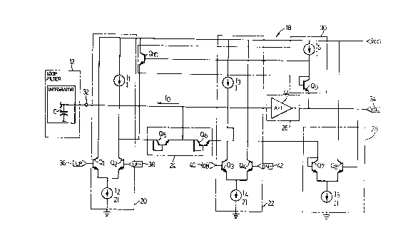
Reference will now be made to Figure 2 which shows in
detail a charge pump topology 18 according to the present invention.
The charge pump topology 18 utilizes only NPN devices for current
switching, and therefore is well suited for a monolithic integrated
circuit implementation. As shov~~n in Figure 2, the charge pump
topology 18 according to the present invention comprises an UP logic
pulse input stage 20, a DOWN logic pulse input stage 22, a
commutating stage 24, a buffer stage 26, a clamping circuit 28, a current
drive stage 30, a loop filter output i:erminal 32 and a voltage controlled
oscillator input terminal 34. The output terminal 32 allows the charge
pump 18 (and output current Io) to be coupled to the loop filter 12. The
loop filter 12 typically includes an integrating capacitor C which
21 13 ~~ 6 2
-5-
converts the output current Io from. the charge pump 18 into a voltage
signal for controlling the voltage controlled oscillator stage 16.
Considering first the LJP logic pulse input stage 20 shown
in Figure 2, the UP pulse input stage 20 comprises a pair of NPN
transistors Ql and Q2, which are emitter coupled to form a differential
pair current switch. As is known in the art, the emitter-coupled
transistor topology offers high speE~d operation because the transistors
do not operate in the saturation region. The base of the first transistor
Q1 provides a non-inverted UP logic pulse input terminal 36, and the
base of the second transistor Q2 is an input terminal 38 for the
inverted UP (UP*) logic pulse input. In known manner, the input
stage 20 includes a current sources h and a current sink IZ. Current
source h connects to the collector of transistor QZ and produces an
internal current I. Current sink I2 connects to the coupled emitters of
transistors Ql and Q2 and sinks a current (2I) which flows in the
emitters of the two transistors Ql and Q2 when they are switched on.
The collector of transistor Q2 provides an output for the UP pulse
input stage 20.
Referring still to Figure 2, the DOWN pulse input stage
22 is very similar to the UP pulse input stage 20 described above. The
DOWN pulse input stage 22 corxiprises two transistors Q3 and Q4
which are also emitter-coupled to form a differential pair current
switch. The base of transistor Q3 provides an input 40 for the non-
inverted DOWN pulse, and the bas.' of transistor Q4 provides an input
42 for the inverted DOWN pulse. The DOWN input stage 22 also
includes a current source I3 and a current sink I4. In known manner,
the current source I3 connects to the collector of transistor Q3 and
produces an internal current I which flows into the collector of
transistor Q3. The current sink I4 connects to the coupled emitters of
transistors Q3 and Q4 and sinks a current 2I which flows from the
emitters of the transistors Q3 and Q4. The collector of transistor Q3
provides an output from the DOWN pulse input stage 22.
21 137 6 2
-6-
The commutating stage 24 comprises two diodes which
can be formed from two diode-connected transistors Q5 and Q6. The
function of the diodes (diode-connected transistors) Q5 and Q6 in the
commutating stage 24 is to correct leakage or drift current when the
charge pump is in one of the idle states (i.e. UP = DOWN =logic 0 or
UP = DOWN = logic 1). The two diode-connected transistors Q5 and
Q6 are coupled between the collector of transistor Q2 and the collector
of transistor Q3. The anode of diode ~Q5 is connected to the collector of
transistor Q2 and the cathode of diode Q5 is connected to the anode of
diode Q6. The cathode of diode Q6 is connected to the collector of
transistor Q3. The loop filter output terminal 32 connects to the node
formed by the connection of the cathode of diode Q5 and the anode of
diode Q6.
Referring still to Figure 2, the current drive stage 30
comprises a drive transistor Qlo, a current source I6 and a diode-
connected transistor Q9 (diode Q9). 7Che emitter of the drive transistor
Qio is connected to the collector of transistor Q2 and the anode of diode
Q5, and the collector of transistor Qlo is connected to the positive
supply rail V~~. The base of transistor Qlo is connected to the anode of
diode Q9 and the output of the current source I6. The current source I6
produces a current I which as will be~ explained is used to generate the
output current Io. The cathode of diode Q9 is connected to the voltage
controlled oscillator terminal 34 and i:he output of the buffer stage 26.
As shown in Figure 2, the buffer stage 26 is connected
between the loop filter output 32 and the VCO terminal 34. In the
preferred embodiment, the buffer ;>tage 26 comprises a unity gain
amplifier 44 having a very high input impedance. The function of the
buffer stage 26 is to buffer the voltage level on the filter output 32 for
use by the drive stage 30 and the clamping circuit 28 to limit the
voltage swing across the diodes Q5 and Q6 in the commutating stage
24.
B
21 137: 6 2 e.
The clamping circuit 28 is coupled between the collector
of transistor Q3 (i.e. the output of the DOWN pulse input stage) and
output of the buffer stage 26 as shown in Figure 2. The function of the
clamping circuit 28 is to limit the voltage swing across the diodes Q5
and Q6 to a voltage of one VBE where VBE is the forward voltage drop
across a base-emitter junction. Th.e clamping circuit 28 comprises a
diode-connected transistor Q~, a transistor Qs and a current sink I5.
The anode of diode Q~ is connected to the cathode of diode Q6 and the
cathode of diode Q~ is connected to the emitter of transistor Q8. The
collector of transistor Q8 is connected to the positive supply rail Vac.
and the base is connected to the VCO terminal 34 (and cathode of
diode Q9). The current sink I5 is connected to the emitters of
transistors Q~ and Q8 and is designErd to sink a current of magnitude 2I.
Typical charge pumps provide an output current Io of
pre-determined polarity in response to the UP and DOWN logic pulses
according to the following truth table:
P OWN o
1 Ip
+Ip
1
As shown in truth table, the charge pump produces the output current
Io (which feeds the loop filter) in two states. The first state occurs
when the UP pulse is logic level 0 and the DOWN pulse is logic level
1. This state is know as the PUMP DOWN state and results in the
charge pump producing a negative output current -Io. The other state
is the PUMP UP state and occurs when the UP pulse is a logic level 1
and the DOWN pulse is at logic level 0. In the PUMP UP state, the
charge pump produces a positive output current Io. The remaining
~1 137 6~2
two states are idle states and in theory the output current Io should be
zero. However in practical implementations, there will be a leakage
current which flows in the output terminal 32. The remainder of the
description will explain the operation of the charge pump 18 according
to the present invention in each of the four staites shown in truth
table.
Reference is first made to Figure ~ which shows the
operation of the charge pump 18 for the idle condition (i.e. UP =
DOWN = 0). When the UP input 36 is at logic level 0, transistor Ql is
off and transistor QZ is on, which results in a currient of magnitude 2I
(where I is the desired output currErnt pulse amplitude) flowing in the
collector of the transistor Q2. The current source h provides half of
the collector current 2I for transistor Q2. Transistor Qlo must provide
the other half (i.e. I) of the collector current in transistor Q2. As can be
shown using Kirchoff's well-known voltage law, transistor Qlo is
turned on because the voltage level at the emitter of transistor Qlo is at
voltage V~, where V~ is the voltage at the output o~ the buffer stage 26,
and therefore the voltage at the ba;>e of transistor Qlo is always V~ +
VBE. This results in a bias voltage across diode Q5 which is very close
to zero, (i.e. V~ + VBE9 - VBEio = «c). hence the current flowing in
diode Q5 will be practically nil. Since the DOWN 40 input is at logic
level zero in this state, transistor Q3 is also off, and hence the current I
produced by current source I3 will flow in diode Q~ (the cathode of
commutating diode Q6 cannot sink current). Tll~e operation of the
clamping circuit 28 (i.e. current sink I5) causes a cuurent of magnitude I
to flow in diode Q~ and an equal current I to flog in the collector of
transistor Qg. This equal splitting of the collector Currents in diode Q~
and transistor Q8 produces base voltages which are equal to voltage V~
and this results in an approximately zero voltage bids across the diodes
Q5 and Q6 which keeps the diodes Q5 and Q6 in the non-conductive
state. In the non-conduction state, the diodes Q5 and Q6 block any flow
of the output current Io to the loop filter 32 which results in extremely
21 137 6 2
-9-
low idle state leakage current which is independent of the output
current Io.
Reference is next made to Figure 4 which shows the
operation of the charge pump 18 for the "PUMP UP" state, i.e. UP =
logic level 1 and DOWN = logic level 0. Since the DOWN input 40 is
at logic level 0, the zero bias condition of diode Q6 is set up in the same
fashion as for the idle condition discussed above. However if the UP
input 36 is at logic level 1, transistor Q2 is turned off, and therefore the
current I from current source I1 will flow into the diode Q5 since the
emitter of Q1o opposes the direction of current flow from current
source h. This causes the voltage level at the emitter of transistor Qlo
to be V~ + VBE. Thus transistor Qlo is zero biased (i.e. turned off) and
therefore provides essentially no current to diode Q5. Since diode Q6
is turned off, the output current Io having a magnitude of I will flow
through diode Q5 to the loop filter output 32 and feed the loop filter
12. It will be appreciated by one skilled in the art that the voltage at the
collector of the transistor Q2 is required to slew through a voltage level
of 1 VBE to turn on the diode Q5 anal allow it to conduct the output
current Io. In the PUMP UP state, diode Q6 remains turned off because
it is reversed biased by the voltage Vc_.
Reference is now made to Figure 5 which shows the
operation of the charge pump 18 in the "PUMP DOWN" state. In the
PUMP DOWN state, the UP input 3E. is at logic level 0 and the DOWN
input 40 is at logic level 1. Since they logic level on the UP* 36 input is
one, transistor Q2 is turned on and the current sink I2 sinks a current
2I (i.e. current source h supplies I and Qlo supplies I). The zero forward
bias condition for diode Q5 is set up in the same fashion as for the idle
condition discussed above. The logic level 0 at the DOWN input 42
keeps transistor Q4 turned off, hence the current sunk by current sink
I4 must flow through transistor Q3. The current source I3 supplies half
of this quantity, i.e. I, and diode 'Q6 sources the remainder, i.e. I to
B
21 137 fi 2
-10-
produce current 2I. This follows because diode Q~ cannot source
current at its anode.
Referring still to Figure 5, when diode Q6 is turned on,
the voltage at its emitter is V~ - VB~E where VBE is the voltage drop
across the base-emitter junction of the diode-connected transistor Q6.
This voltage produces an essentially zero bias condition for diode Q~,
and therefore diode Q~ remains turned off and provides no
conduction path for additional current flow. Since diode Q5 is off and
diode Q6 is on, it follows that the output current Io will flow into
diode Q6 resulting in a negative output current Io being supplied to
the loop filter 12. It will be appreciated that the voltage at the collector
of transistor Q3 is required to slew through a voltage of VBE to bring
diode Q6 into conduction (as was the case for transistor Q2 in the
"PUMP UP" state discussed above).
It will be appreciated by one skilled in the art that net
current available to charge the nodes at the respective collectors of
transistors Q2 and Q3 is current I. Therefore, to preserve symmetry of
response for both UP and DOWN pu:Lses, the parasitic loading at these
nodes must also be essentially the same for both nodes. Referring to
Figure 5, the node at the collector of transistor QZ has a tally of 2
collectors (Q2 and Q5), 1 emitter (Q1o), and 1 current source (h) which
produces a current with magnitude I. The tally for the node at the
collector of transistor Q3 is also 2 collectors (Q3 and Q~), 1 emitter (Q6)
and 1 current source (I3).
Figure 6 shows the situation when the UP and DOWN
pulses are both active high. This is referred to as "ALT IDLE"
(alternate idle). Although both logic pulses are active high, the charge
pump is expected to produce no output current Io. This situation only
occurs with certain implementations of phase/frequency detectors,
and is much less critical for output leakage performance than the true
idle condition (UP = DOWN = 0) discussed above. In ALT IDLE state,
the output current Io is the difference between the currents flowing in
B
___ 2113762
-11-
diode Q5 and diode Q6, and consequently the output current Io which
leaks will not be as low as for the idle state discussed above. However
for most applications, this resulting leakage current does not present a
problem.
It will be evident to those skilled in the art that while
preferred embodiments of the charge pump topology of the present
invention have been described, the scope of the present invention is
intended to be defined by the following claims.
B