Sélection de la langue

Search

Sommaire du brevet 2114880 

Énoncé de désistement de responsabilité concernant l'information provenant de tiers

Une partie des informations de ce site Web a été fournie par des sources externes. Le gouvernement du Canada n'assume aucune responsabilité concernant la précision, l'actualité ou la fiabilité des informations fournies par les sources externes. Les utilisateurs qui désirent employer cette information devraient consulter directement la source des informations. Le contenu fourni par les sources externes n'est pas assujetti aux exigences sur les langues officielles, la protection des renseignements personnels et l'accessibilité.

Disponibilité de l'Abrégé et des Revendications

L'apparition de différences dans le texte et l'image des Revendications et de l'Abrégé dépend du moment auquel le document est publié. Les textes des Revendications et de l'Abrégé sont affichés :

  • lorsque la demande peut être examinée par le public;
  • lorsque le brevet est émis (délivrance).
(12) Brevet: (11) CA 2114880
(54) Titre français: CIRCUIT DE CORRECTION DU NIVEAU DU NOIR POUR SYSTEME D'AFFICHAGE VIDEO
(54) Titre anglais: BLACK COMPENSATION CIRCUIT FOR A VIDEO DISPLAY SYSTEM
Statut: Périmé et au-delà du délai pour l’annulation
Données bibliographiques
(51) Classification internationale des brevets (CIB):
(72) Inventeurs :
  • WHITE, CHARLES MICHAEL (Etats-Unis d'Amérique)
  • GURLEY, THOMAS DAVID (Etats-Unis d'Amérique)
(73) Titulaires :
  • THOMSON CONSUMER ELECTRONICS, INC.
(71) Demandeurs :
  • THOMSON CONSUMER ELECTRONICS, INC. (Etats-Unis d'Amérique)
(74) Agent: CRAIG WILSON AND COMPANY
(74) Co-agent:
(45) Délivré: 2003-07-15
(22) Date de dépôt: 1994-02-03
(41) Mise à la disponibilité du public: 1994-08-06
Requête d'examen: 2001-01-18
Licence disponible: S.O.
Cédé au domaine public: S.O.
(25) Langue des documents déposés: Anglais

Traité de coopération en matière de brevets (PCT): Non

(30) Données de priorité de la demande:
Numéro de la demande Pays / territoire Date
014,156 (Etats-Unis d'Amérique) 1993-02-05

Abrégés

Abrégé anglais


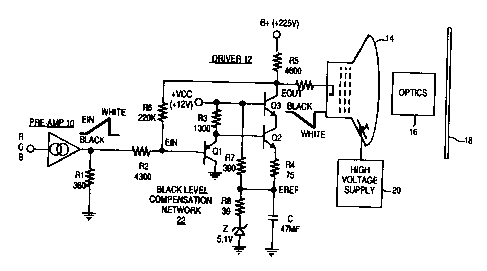
A driver for a cathode ray tube includes a black level
compensation circuit which generates an offset voltage which
tracks the current flowing to the output of the driver and
therefore the average picture level (APL). The offset voltage is
added as a component of the output voltage so as to increasingly
shift the output voltage toward black as the APL increases. This
compensates for CRT gamma non-linearities and for light
scattering effects which might otherwise cause the loss of
perceived detail and sharpness in dark areas of a high APL image.
In the disclosed embodiment, the driver comprises a cascode
amplifier and the offset voltage generating element includes a
capacitively bypassed resistor connected in a reference voltage
network connected to the emitter circuit of the lower (common
emitter configured) transistor of the cacode amplilfier.

Revendications

Note : Les revendications sont présentées dans la langue officielle dans laquelle elles ont été soumises.


-6-
Claims
1. In a video display system having a cathode ray tube
for displaying an image, apparatus comprising:
a video output amplifier for amplifying a relatively low
level video input signal received at an input of said video output
amplifier to produce a relatively high level video output voltage
suitable for direct application to a cathode ray tube at an output of
said video output amplifier;
means coupled to an output current path of said video
output amplifier for generating a reference voltage in response to
the current flowing in said current path and representative of the
average picture level of said image; and
means for coupling an offset signal responsive to said
reference voltage to said output of said video output amplifier.
2. The apparatus recited in claim 1, wherein:
said video output amplifier includes a transistor having
a current path between first and second electrodes, and a control
electrode for controlling the conduction of said current path, said
video input signal being coupled to said control electrode, the
second electrode being coupled to said output of said video output
amplifier; and
said means for generating said reference voltage
includes a DC impedance element and a low pass filter element, and
means for coupling said DC impedance element to said first
electrode.
3. The apparatus recited in claim 2, wherein:

-7-
said means for coupling said offset signal to said output
of said video output amplifier comprises said means for coupling
said impedance element to said first electrode.
4. The apparatus recited in claim 3, wherein:
said video output amplifier includes a second transistor
having a current path between first and second electrodes, and a
control electrode for controlling the conduction of said current path,
a DC voltage being coupled to said control electrode of said second
transistor, said second electrode of said second transistor being
coupled to said output of said video output amplifier, and said
second electrode of said first mentioned transistor being coupled to
said first electrode of said second transistor and thereby being
coupled by said current of said second transistor to said output of
said video output amplifier.
5. The apparatus recited in claim 2, wherein:
said means for generating said reference voltage further
includes means for providing a fixed DC voltage, said DC impedance
being coupled in a series path with said means for providing said
fixed DC voltage; and said low pass filter element is coupled in
parallel with said series path.
6. The apparatus recited in claim 5, wherein:
said means for coupling said DC impedance element to
said first electrode comprises a second DC impedance element.
7. The apparatus recited in claim 6, wherein:
said first mentioned DC impedance element comprises a
first resistor; said means for providing said fixed DC voltage

-8-
comprises a Zener diode; said low pass filter element comprises a
capacitor; and said second DC impedance element comprises a
second resistor coupled in series between said first resistor and said
first electrode.
8. In a video system, apparatus comprising:
a video amplifier for amplifying a video input signal
received at an input to produce a video output signal representative
of an image at an output;
said video amplifier including a transistor having a
current path between first and second electrodes, and a control
electrode for controlling the conduction of said current path, said
video input signal being coupled to said control electrode, the
second electrode being coupled to said output of said video output
amplifier;
means coupled to an output current path of said video
amplifier for generating a reference signal in response to the
current flowing in said current path and representative of the
average picture level of said image;
said means for generating said reference signal
including a DC impedance element and a low pass filter element,
and means for coupling said DC impedance element to said first
electrode of said transistor; and
means for coupling an offset signal corresponding to
said reference signal to said output of said video output amplifier.

Description

Note : Les descriptions sont présentées dans la langue officielle dans laquelle elles ont été soumises.


-1- RCA 87,003
BLACK COMPENSATION CIRCUIT FOR A V>DEO DISPLAY SYSTEM
The invention concerns an arrangement for driving a
display device, such as a cathode ray tube (CRT), with provisions
for automatically adjusting the black level of a reproduced image
as a function of the average picture level of the image. In
television receivers, especially projection type television
receivers, management of the black level of the reproduced image
is critical to maintaining perceived detail and sharpness in dark
image portions. Unfortunately, the electro-optic characteristics of
the CRT itself, and in the case of projection type television
receiver, the optical system itself, interferes with the faithful
reproduction of dark image portion. This is primarily due to the
non-linearity or "gamma" of the CRT, and also to light scattering
1 S effects, especially in a projection television receiver.
Gamma refers to the non-linear voltage drive to light
output of the CRT. When the television transmission standard was
originally defined, television cameras were designed to have a
complimentary gamma function to that of CRTs so that the overall
2 0 transmission system from camera light input to CRT light output
was linear. However, as time went on, CRTs were designed for
more and more light output, resulting in a in a different (higher)
gamma than the one of earlier CRTs. Cameras, however continue
to conform more or less to the original defined gamma
2 5 characteristics for television cameras. Thus, the modern television
receivers exhibit a non-linear light output characteristic relative
to the original scene scanned by the television camera. The result
of this mis-match in gammas between the camera and the CRT is
that low level luminance scenes are displayed with less contrast
3 0 than the original scene and high level luminance scenes with more
contrast than the original scene.
Unnaturally high contrast areas of the picture are
rarely complained about. However, there may be a loss of
perceived detail and sharpness in low light areas having
3 S unnaturally low contrast. This situation could be corrected by
adding gamma correction circuitry to the television receiver to
bring the effective gamma of the television receiver back closer to
the one contemplated by the original television transmission

- z - ~ ~- ~ ~ ~ ~ ~ RCA 87,003
standard. However, this is rarely done because of circuit
complexity and cost. In addition, gamma correction tends to
enhance noise in the low light areas of the reproduced image
relative to an arrangement without gamma correction. This
results because noise introduced in the transmission path is
amplified by the gamma corrector.
The second phenomena which adversely affects
perceived low light area image detail and sharpness, light-
scattering, is due to light from high light areas spilling into all
areas causing black areas to appear less black. With images
having a significant high light image portion i.e., images with a so
called high average picture level (APL), light scattering may result
in loss of detail in dark areas. Light scattering is typically a more
severe problem in a projection television systems due to their
optics.
In accordance with an aspect of the invention, it is
recognized that one relatively simple way of reducing the
objectionable effects from both uncorrected gamma of the CRT and
light-scattering, is to cause black levels to become "more black"
2 0 when the image has a high APL and to become less black (whiter)
when the image has a low APL. This has the effect of restoring
perceived detail and sharpness in dark areas of an image with a
high APL in which light-scattering would otherwise tend to "wash
out" the dark area details. This technique also tends to shift low
2 5 light images up in light level so that contrast in these scenes is
less compressed by the non-linear gamma characteristics of the
QtT.
Another aspect of invention concerns the manner in
which the above described technique may be simply implemented
3 0 in the CRT drive stage, as shown by way of example in the sole
Figure of the accompanying Drawing.
The sole Figure is a schematic of the video output
section of a projection television system including a black level
compensation arrangement constructed in accordance with the
3 5 invention.
The output section shown in the sole Figure is one of
three such sections employed in a projection television system,
each for developing an image corresponding to a respective one of

- 3 - 2 ~ ~ ~ ~ c~ ~ RCA 87,003
a red (R), green (G) or blue (B) video signal. The other two
sections are not shown since they are are substantially identical to
the one which is shown. Typical component values and voltages
are indicated in the Figure by way of example. Resistor values are
in ohms unless otherwise indicated. The letter "K" stands for
kilohms and the letters "MF" stand for microfarads.
A processed video signal (either red, green or blue) in
the form of a voltage is coupled to the input of a preamplifier 10.
Preamplifier 10 is a current amplifier which converts the video
input voltage to a corresponding output current. The output
current is in turn converted to an input voltage EIN for video
output amplifier or CRT driver 12 by a terminating resistor Rl.
CRT driver 12 amplifies the relatively low input voltage EIN to
produce a relatively high level output voltage EOUT which is
1 5 coupled to the cathode of a projection CRT 14. The light output of
CRT 14 is transmitted by an optics section 16 to a screen 18,
where it is combined with the light outputs of the other two
output sections to display a composite color image. A high voltage
stage 20 provides a very high supply voltage to the anode of CRT
2 0 14, as well as relatively lower voltages to various grids of CRT 14.
Driver 12 comprises an emitter-follower amplifier
including PNP transistor Q1 and a cascode amplifier including NPN
transistors Q2 and Q3. Input voltage EIN is coupled by a resistor
R2 to the base of transistor Q1, where a voltage EIN' is developed.
2 5 The emitter of transistor Q1 is coupled to the base of transistor Q2.
A resistor R3 coupled between the emitter of transistor Q1 and a
source of supply voltage +VCC serves as a load resistor for
emitter-follower configured transistor Q1. Transistor Q2 is
configured as a common emitter amplifier, providing an output
3 0 current at its collector which is coupled to the emitter of transistor
Q3. Resistor R4 is coupled between the emitter of transistor Q2
and a black level compensation network 22 which develops a
reference voltage EREF dependent on the average picture level, as
will be described in detail below. Transistor Q3 is configured as a
3 S common base amplifier, having supply voltage +VCC coupled to its
base and providing the output voltage EOUT at its collector.
Output voltage EOUT is developed across a load, represented
simply as a resistor R5, connected between the collector of

- 4 - RCA 87,003
2~.~.~~~z~!
transistor Q3 and a source of supply voltage B+. It will be
appreciated by those skilled in the art that the load of driver 12
may be more complex and may include active devices. For
example the load of driver 12 may comprise complementary
transistors configured as respective emitter-follower amplifiers
and connected in a "push-pull" arrangement. Resistor R6 is
coupled between the output of driver 12 at the collector of
transistor Q3 and the base of transistor Q1, and together with
resistor R2 provides negative feedback to the input of driver 12.
1 0 The overall gain of driver 12 is primarily set by resistors R2, R4,
RS and R6.
Black level compensation network 22 comprises a
resistor R7, a resistor R8 and a Zener diode Z connected in series
between the source of supply voltage +VCC and a point of signal
ground, and a filter capacitor C connected in parallel with the
series combination of resistor R8 and Zener diode Z. Reference
voltage EREF is the sum of the Zener voltage developed by Zener
diode Z and the voltage developed across resistor R8. The voltage
developed by Zener diode Z establishes a nominal value for
2 0 reference voltage EREF. The current which flows through resistor
R8 is primarily provided from the output of driver 12 through
transistors Q2 and Q3 and resistor R4. Capacitor C removes the AC
signal component from reference voltage EREF. The current
provided from the output of driver 12, and which flows through
2 S resistor R8, increases as the as the average picture level (APL)
increases and image becomes lighter, and decreases as the APL
decreases and the image becomes darker. Thus, reference voltage
EREF increases as the APL increases and decreases as the APL
decreases.
3 0 The output voltage EOUT is approximately expressed
as:
EOUT = (B+) - (EIN' - EREF) (RS/R4)
Accordingly, voltage EOUT increases as the APL and voltage EREF
increase. This causes CRT 14 to move closer to cut off and thereby
3 5 makes the black level mare black. Thus, the possibility of the loss
of perceived detail and sharpness in dark portions of a high APL
image due the gamma non-linearity of CRT 14 and the light
scattering produced by optics 16 and screen 18 are reduced.

- 5 - ~ ~ 1 ~ ~ a ~ RCA 87,003
Conversely, voltage EOUT decreases as the APL and voltage EREF
decrease. This causes CRT 14 to move away from cut off and
thereby makes the black level less black.
Black level compensation network 22 operates by
generating a black level offset voltage, (EREF)(RS/R4), which is
responsive to the current flowing in driver 12, and therefore the
APL, and which is coupled to the output of driver 12 so as to be a
component of output voltage EOUT. While the black level is
changed, there is no corresponding change of the AC gain of driver
12 and the linearity of driver 12 is maintained.
While the invention has been described in terms of a
projection television system, it is noted that is also useful in a
direct view television system. Further, while preamplifier 10 of
the described embodiment comprises a current amplifier, it could
1 S also comprise a voltage amplifier. Still further, configurations of
drivers other than a cascode amplifier may be employed. These
and other modifications are intended to be within the scope of the
invention defined by the following claims.

Dessin représentatif
Une figure unique qui représente un dessin illustrant l'invention.
États administratifs

2024-08-01 : Dans le cadre de la transition vers les Brevets de nouvelle génération (BNG), la base de données sur les brevets canadiens (BDBC) contient désormais un Historique d'événement plus détaillé, qui reproduit le Journal des événements de notre nouvelle solution interne.

Veuillez noter que les événements débutant par « Inactive : » se réfèrent à des événements qui ne sont plus utilisés dans notre nouvelle solution interne.

Pour une meilleure compréhension de l'état de la demande ou brevet qui figure sur cette page, la rubrique Mise en garde , et les descriptions de Brevet , Historique d'événement , Taxes périodiques et Historique des paiements devraient être consultées.

Historique d'événement

Description Date
Inactive : CIB expirée 2023-01-01
Inactive : CIB de MCD 2006-03-11
Le délai pour l'annulation est expiré 2005-02-03
Lettre envoyée 2004-02-03
Accordé par délivrance 2003-07-15
Inactive : Page couverture publiée 2003-07-14
Inactive : Taxe finale reçue 2003-04-24
Préoctroi 2003-04-24
Lettre envoyée 2002-11-13
Un avis d'acceptation est envoyé 2002-11-13
Inactive : Approuvée aux fins d'acceptation (AFA) 2002-10-30
Lettre envoyée 2001-02-14
Inactive : Renseign. sur l'état - Complets dès date d'ent. journ. 2001-02-14
Inactive : Dem. traitée sur TS dès date d'ent. journal 2001-02-14
Toutes les exigences pour l'examen - jugée conforme 2001-01-18
Exigences pour une requête d'examen - jugée conforme 2001-01-18
Modification reçue - modification volontaire 2001-01-18
Demande publiée (accessible au public) 1994-08-06

Historique d'abandonnement

Il n'y a pas d'historique d'abandonnement

Taxes périodiques

Le dernier paiement a été reçu le 2003-01-23

Avis : Si le paiement en totalité n'a pas été reçu au plus tard à la date indiquée, une taxe supplémentaire peut être imposée, soit une des taxes suivantes :

  • taxe de rétablissement ;
  • taxe pour paiement en souffrance ; ou
  • taxe additionnelle pour le renversement d'une péremption réputée.

Les taxes sur les brevets sont ajustées au 1er janvier de chaque année. Les montants ci-dessus sont les montants actuels s'ils sont reçus au plus tard le 31 décembre de l'année en cours.
Veuillez vous référer à la page web des taxes sur les brevets de l'OPIC pour voir tous les montants actuels des taxes.

Historique des taxes

Type de taxes Anniversaire Échéance Date payée
TM (demande, 4e anniv.) - générale 04 1998-02-03 1998-01-22
TM (demande, 5e anniv.) - générale 05 1999-02-03 1999-01-21
TM (demande, 6e anniv.) - générale 06 2000-02-03 1999-12-23
TM (demande, 7e anniv.) - générale 07 2001-02-05 2001-01-18
Requête d'examen - générale 2001-01-18
TM (demande, 8e anniv.) - générale 08 2002-02-04 2002-01-24
TM (demande, 9e anniv.) - générale 09 2003-02-03 2003-01-23
Taxe finale - générale 2003-04-24
Titulaires au dossier

Les titulaires actuels et antérieures au dossier sont affichés en ordre alphabétique.

Titulaires actuels au dossier
THOMSON CONSUMER ELECTRONICS, INC.
Titulaires antérieures au dossier
CHARLES MICHAEL WHITE
THOMAS DAVID GURLEY
Les propriétaires antérieurs qui ne figurent pas dans la liste des « Propriétaires au dossier » apparaîtront dans d'autres documents au dossier.
Documents

Pour visionner les fichiers sélectionnés, entrer le code reCAPTCHA :


Pour visualiser une image, cliquer sur un lien dans la colonne description du document. Pour télécharger l'image (les images), cliquer l'une ou plusieurs cases à cocher dans la première colonne et ensuite cliquer sur le bouton "Télécharger sélection en format PDF (archive Zip)" ou le bouton "Télécharger sélection (en un fichier PDF fusionné)".

Liste des documents de brevet publiés et non publiés sur la BDBC .

Si vous avez des difficultés à accéder au contenu, veuillez communiquer avec le Centre de services à la clientèle au 1-866-997-1936, ou envoyer un courriel au Centre de service à la clientèle de l'OPIC.


Description du
Document 
Date
(aaaa-mm-jj) 
Nombre de pages   Taille de l'image (Ko) 
Dessin représentatif 2003-06-10 1 11
Revendications 1995-06-08 2 89
Abrégé 1995-06-08 1 18
Description 1995-06-08 5 208
Dessins 1995-06-08 1 13
Revendications 2001-02-21 3 107
Dessin représentatif 1998-08-24 1 13
Rappel - requête d'examen 2000-10-03 1 116
Accusé de réception de la requête d'examen 2001-02-13 1 179
Avis du commissaire - Demande jugée acceptable 2002-11-12 1 163
Avis concernant la taxe de maintien 2004-03-29 1 173
Correspondance 2003-04-23 1 29
Taxes 1997-01-29 1 58
Taxes 1996-01-03 1 53