Note : Les descriptions sont présentées dans la langue officielle dans laquelle elles ont été soumises.
,..~
SEI 93-42
TITLE OF THE INVENTION
Field Effect Transistor and Method of Manufacturing
the Same
BACK~ROUND OF THE INVENTION
._ _
Field of the Invention
,~
The present invention relates to the structure of a
field effect transistor (FET) which can realize an ultra
high-speed operation, and a method of manufacturing the
same.
Related Background Art
Conventionally, as an FET which can realize an ultra
high-speed operation, an EET in which an active layer for
.
forming a current channel adopts a so-called pulse doped
structure is known. In the FET with the pulse-doped
structure, the impurity profile of the active layer
reveals an undoped state from the substrate surface to a
predetermined depth. However, the impurity concentration
changes in a pulse-like pattern or stepwise to a high
concentration at the predetermined depth from the
substrate surface, and the impurity profile returns to an
undoped state at a deeper substrate position. Such an FET
with the pulse-doped structure is described in, eOg.,
U.S. Patent No. 4,163,984 or in p. 759 of the following
reference:
1986 IEEE IEDM "A 760 mS/mm N+SELF-ALIGNED
ENHANCEMENT MODE DOPED-CHANNEL MIS-LIKE FET(DMT)"
~ ' 1
~.
B 8 8
SEI 93-42
However, in such an FET with the pulse-doped
structure, a sufficient quantity of electrons for forming
a current channel cannot be assured. For this reason,
another patent application (Japanese Patent Laid-Open
No. 4-245646) by the present applicant proposed an FET
having a pulse-doped structure in which two active layers
are formed. With this FET, since the two active layers
are formed, the quantity of electrons for forming a
. . .
current channel increases, and a high current output can
be realized.
However, in the conventional FET with the structure
including two active layers, when a long gate effect
; occurs due to a surface depletion layer in the drain
electrode side, the effective gate length increases, and -
the active layer formed on the surface side of the
substrate is depleted. When the active layer is
. depleted, the flow of channel electrons is hindered, and
the total quantity of electrons for forming a current
channel decreases. As a result, a high current output
cannot often be obtained in the conventional FET with the
!' above-mentioned structure.
In the conventional FET with the pulse-doped
structure described in the above-mentioned U.S. Patent,
electrons for forming a channel move in an active layer
with a high impurity concentration in a low electric
field region. For this reason, electrons are
,
~:
~,'
211 ~088
SEI 93--42
considerably influenced ~y impurity scattering, and the
electron mobility in a low electric field region is
lowered. As a result, the high-fre~uency operation
characteristics of an element cannot be improved. ~
transconductance gm which represents the rate of change in
drain current with respect to a change in gate voltage
cannot hold a constant value over a given range with
respect to a change in gate voltage.
SUMMARY OF THE INVENTION
The present invention has been made to solve the
above-mentioned problems, and has as its object to
provide an FET usin~ a thin-film semiconductor layer
having a high impurity concentration as a channel layer,
wherein the channel layer is formed with three or more
iabove semiconductor layers to sandwich an undoped layex
betwaen each two adjacent semiconductor layers.
In an FET with the structure of the present
; invention, extension of a surface depletion layer from
the substrate surface to a deep portion is disturbed by
the semiconductor layer closest to the substrate surface.
Three or more semiconductor layers constituting the
channel layer are formed to sandwich an undoped layer
between each two adjacent semiconductor layers, and a
plurality of semiconductor layers are formed in a
semiconductor substrate position deeper than the
semiconductor layer closest to the substrate surface.
,
: I .
;,
, ~ ., .. , ~ .. . . . . . ., . -
SEI 93-42
For this reason, even when the semiconductor layer
closest to the substrate surface is depleted, a
sufficient quantity of electrons for forming a current
channel can be assured.
According to the present invention, in an FET using
a thin-film semiconductor layer having a high impurity
concentration as a channel layer, a plurality of above
semiconductor layers constituting the channel layer are
formed to sandwich an undoped layer between each two
adjacent semiconductor layers, a doping layer is formed
on a semiconductor layer, closest to the substrate
surface, of these semiconductor layers via an undoped
layer, and the doping layer has a predetermined impurity
concentration and thickness so as to prevent a surface
depletion layer from spreading to the channel layer.
In this manner, when the doping layer having the
predetermined impurity concentration and thickness is
formed on the channel layer closest to the substrate
surface, e~tension of the surface depletion layer from
the substrate surface to a deep portion is disturbed by
the doping layer formed on the channel layer. Since the
plurality of semiconductor layers constituting the
channel layer are formed below the doping layer, a
sufficient quantity of electrons for forming a current
channel can be assured.
For this reason, in the FET with the structure
I .:
. .
SEI 93-42
according to the present invention, a sufficient quantity
o electrons for forming a current channel can be assured
by the plurality of semiconductor layers constituting the
channel layer. Therefore, a sufficiently high output
current is maintained without being influenced by a
surface depletion layer, and an FET which can realize a
high-output, high-speed operation can be provided.
According to the present invention, in an FET using
~ a thin-film semiconductor layer having a high impurity
-! lo concentration as a channel layer, a plurality of
semiconductor layers are formed to constitute the channel
layer, and an intermediate concentration layer having a
lower impurity concentration than that of the
semiconductor layers is formed ~etween each two adjacent
semiconductor layers.
In the FET in which the intermediate concentration
layer is formed between each two adjacent ones of the
plurality of semiconductor layers, since the intermediate
concentration layer has a low impurity concentration,
channel electrons are also generated by an impurity
present in the intermediate concentration layer.
Therefore, electrons for forming a current channel are
distributed in the intermediate concentration layer
¦ between each two adjacent semiconductor layers even in a
low electric field region, and move in the intermediate
concentration layer having a lower impurity concentration
.
SEI 93-42
,~
than that of the semiconductor layers forming the
channel.
I For this reason, the mobility of channel electrons
in the low electric field region increases, and a high
electron saturation rate is maintained, thus improving
the high-frequency characteristics of an element. Also,
a transconductance gm can hold a constant value over a
given range with respect to a change in gate voltage.
According to the present invention, a method of
manufacturing an FET in which a channel layer is formed by
the step of forming an undoped layer, the step of forming
a thin-~ilm semiconductor layer having a high impurity
concentration on the undoped layer, and the step of
forming an undoped layer on the semiconductor layer,
comprises the step of forming the channel layer by
forming a plurality of the semiconductor layers
sandwiched between tha undoped layers by repeating the
step of forming the undoped layer and the step of forming
the semiconductor layer, and the step of forming an
intermediate layer by diffusing an impurity contained in
the semiconductor layers to the undoped layers by
performing annealing after these steps.
When the int~rmediate concentration layer is formed
by annealing, layers which sandwich the plurality of
semiconductor layers at the outermost sides contain an
impurity at a low concentration, and channel electrons
. . ..
8 8
SEI 93-42
are distributed to the two outermost layers as well.
Therefore, channel electrons move in the two outermost
layers having a low impurity concentration in addition to
the intermediate concentration layer.
For this reason, the mobility of channel electrons
in a low electric field region can be further increased,
and the high-frequency characteristics of an element can
be further improved.
Also, according to the present invention, a method
of manufacturing an FET comprises the step of forming an
intermediate concentration layer, the step of forming a
thin-film semiconductor layer having a high impurity
concentration on the intermediate concentration layer,
and the step of forming an intermediate concentration
layer on the semiconductor layer, wherein the
intermediate concentration layer is formed to have an
; impurity concentration lower than that of the
¦ semiconductor layer by a crystal growth method in which,
an impurity concentration is controlled, and the channel
layer is formed by forming a plurality of the
semiconductor layers each of which is sandwiched between
the intermediate concentration layers by repeating the
step of forming the intermediate concentration layer and
the step of forming the semiconductor layer.
~; The present invention will become more ~ully
understood from the detailed description given -~
'
:',`,
SEI 93-42
hereinbelow and the accompanying drawings which are given
by way of illustration only, and thus are not to be
considered as limiting the present invention.
Further scope of applicability of the present
.~ invention will become apparent from the detailed
description giv~n hereinafter. However, it should be
understood that the detailed description and specific
examples, while indicating preferred embodiments of the
invention, are given by way of illustration only, since
various changes and modifica~ions within the spirit and
scope of th~ invention will become apparent ~o those
skilled in the art form this detailed description.
BRIEF DESCRIPTION OF THE DRAWINGS
FIGs. 1 to 3 are sectional views showing the
processes in the manufacture of an FET according to the
first embodiment of the present invention;
FIG. 4 is a graph showing the impurity profile below
the gate electrode of the FET according to the first
embodiment;
FIG. 5 is a sectional view showing a conventional
FET having a single-channel structure to be compared with
'the FET of the first embodiment so as to show effects of
the FET of the first embodiment;
! FIG. 6 is a graph showing the characteristics of the
FET of the first embodiment;
FIG. 7 is a graph showing the characteristics of the
~ 8
~ 6 08~
:' SEI 93-42
conventional FET shown in FIG. 5;
FIG. 8 is a sectional view showing the structure of
an FET according to the second embodiment of the present
invention;
FIG. 9 is a sectional view ~howing the structure of
~n FET according to the third embodiment of the present
invention;
FIGs. 10 to 13 are sectional views showing the
~ processes in the manufacture of the FET according to the
``~l 10 third embodiment; and
FIG. 14 is a graph showing the impurity profile
. below the gate electrode of the FET according to the third
embodiment.
DETAILED DESCRIPTION OF THE PREFERRED EMBODIMENTS
. _ _ _ . _ .. . . .
FIGs. 1 to 3 are sectional views showing the method
of manufacturing an FET according to the first embodiment
of the present invention. -
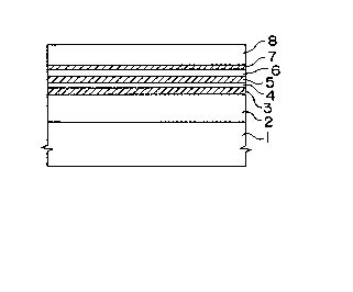
Semiconductor layers (to be described below) are
sequentially deposited on a semi-insulating GaAs
semiconductor substrate 1 by an epitaxy technique such as
an MBE ~Molecular Beam Epitaxy) method, an OMVPE (Organic
~Metal Vapor phase Epitaxy) method, or the like. An
undoped GaAs buffer layer 2 is epita~ially grown on the
GaAs substrate 1. When the FET is formed by the OMYPE
method, the buffer layer 2 is set to be an undoped layer
having p~ background conductivity type by controlling the :~
.11 9
~1
;~l
SEI 93-42
supply ratio of Ga as a Group-III material and As as a
Group-V material. The impurity concentration of the
layer 2 is suppressed to as low as 5 x 1ol6 [cm~3] or less.
Then, an Si-doped GaAs layer is epitaxially grown on
the buffer layer 2 to form a first channel layer 3 as a
first semiconductor layer. The first channel layer 3
contains Si ions as an n~type impurity at a high
concentration of about 3 x lol8 [cm~3], and has a thickness
as small as 80 A. Subsequently, a 50-A thick first spacer
layer 4 consisting of undoped GaAs is epitaxially grown
on the first channel layer 3. The background
conductivity type of the first spacer layer 4, when th~
FET is formed by the OMVPE method, is n~ type, and its
impurity concentration is suppressed to as low as 5 x 10¹⁵
[cm~3] or less. Note that, when the FET is formed by the
MBE method, the background conductivity type of the first
spacer layer 4 is p~ type.
Furthermore, a second channel layer 5 as a second
semiconductor layer, a second spacer layer 6, a third
channel layer 7 as a third semiconductor layer, and a
capping layer 8 are sequentially epitaxially grown on the
first spacer layer 4 (see FIG. 1). These second and third
channel layers 5 and 7 are formed by using Si-doped GaAs
having the same impurity concentration as that of the
first channel layer 3 to have thicknesses of 70 A and 80
A, respectively. The second spacer layer 6 is formed
..
.:
. .
21~ 6~8
SEI 93-42
using the same undoped GaAs as in the first spacer layer 4
to have the same thickness as that of the layer 4. The
capping layer 8 is formed using the same undoped GaAs as
in the spacer layers 4 and 6. In this case, the capping
layer 8 .is formed to have a thickness, i.e., a depth, from
the substrate surface to the third channel layer 7, of
400 A.
A source-drain region pattern is formed on the
substrate surface using a lithography technique, and
high-concentration Si ions are selectively ion-implanted
using this pattern as a mask. By this selective ion
implantation, an n+-type drain region 9 and an n+-type
source region 10 are formed. Then, a gate electrode 11 is
formed using, e.g., a deposition technique, lithography
technique, etching technique, and the like (see FIG. 2).
The gate electrode 11 is formed at a position separated
away from the drain region 9.
Finally, a drain electrode 12 and a source electrode
13, which respectively ohmic-contact the drain region 9
and the source region 10, are formad using a similar
deposition technique, lithography technique, and the
like. Upon formation of these electrodes, a Schottky
contact type FET (MESFET) is completed (see FIG. 3).
The impurity profile below the gate electrode 11 of
this embodiment is as shown in the graph in FIG. 4. The
abscissa of the graph in FIG. 4 represents a depth d [~m]
11
, f-\-
2 ~ 8 ~3
;~
SEI 93-42
from the substrate surface, and the ordinate represents a
COnCQntratiOn ND ~cm~3] of an n-type impurity, Si. In this
impurity profile, the impurity concentration locally
increases in a pulse pattern. A pulse-pattern portion
near the substrate surface represents a profile
corresponding to the third channel layer 7 having a high
impurity concentration, a pulse-pattern portion adjacent
to this represents a profile corresponding to the second
channel layer 5 having a high impurity concentration, and
a pulse-pattern portion in the substrate deep portion
represents à profile corresponding to the first channel
layer 3.
In the FET of this embodiment, even when a surface
.
depletion layer is formed due to the interface level of
the substrate surface on the side of the drain electrode
12, e~ctension of the surface depletion layer to a deeper
portion in the substrate is prevented by the third
channel layer 7 closest to the substrate surface side.
The two channel layers, i.e., the second and first
channel layers 5 and 3 are formed at substrate positions
deeper than the third channel layer 7. Therefore, even
when electrons moving in the third channel layer 7 are
shielded by the surface depletion layer, a sufficient
quantity of channel electrons are assured by the impurity
present in the second and first channel layers 5 and 3 at
a high concentration.
12
8 ~
SEI 93-42
More specifically, when a low electric field is
applied across the drain-source path, a part of a large
quantity of electrons generated in the plurality of
channel layers 5 and 3 are present with a high probability
in the second and first spacer layers 6 and 4 and the --
buffer layer 2 as undoped layers with good electron
transfer characteristics. For this reason, many
electrons move along the source-drain pa~h at high speed
without being influenced by impurity scattering. When a
high electric field is applied across the drain~source
path, more electrons constituting the channel acquire a
higher energy level and move into the undoped spacer
layers 6 and 4 and the undoped buffer layer 2, which
sandwich the channel layers 5 and 3 therebetween and have
good electron transfer characteristics. For this reason,
again, a large quantity of electrons move acrosæ the
drain-source path without being influenced by impurity
scattering. As a result, as compared with a conventional
FET formed with only two channel layers, the probability
of the presence of carriers in the spacer layers 6 and 4
and the buffer layer 2 with good electron transfer
characteristics increases, and a sufficiently high output
current is maintained without being influenced by the ;
surface depletion layer. Therefore, a problem of a low
current output is not posed unlike in the conventional ~-~
FET.
13
~'
'.
0 ~ 8
SEI 93-42
The characteristics of thP FET with ~he pulse-doped
structure according to this embodiment in which a channel
layer is formed by arranging three thin-film
semiconductor layers having a high impurity
concentration, will be compared below with those of a
conventional FET with a pulse-doped structure in which
only one semiconductor layer is formed in a channel
layer.
The conventional FET with the pulse-doped structure
has a sectional structure shown in FIG. 5. More
specifically, an undoped GaAs buffer layer 22 of p~
background conductivity type is formed on a
semi-insulating GaAs semiconductor substrate 21. A
channel layer 23 containing an Si impurity at a high
concentration is formed on the buffer layer 22. The
impurity concentration of the channel layer 23 is 3 x 10
[cm~3], and its thickness is 230 A. Furthermore, a 400-A
thick capping layer 24 consisting of an undoped GaAs
layer of n~background conductivity type is formed on the
. 20 channel layer 23. An n~-type drain region ~5 and an
n+-type source region 26 are formed to sandwich the
channel layer 23 therebetween, a gate electrode 27 is
formed to Schottky-contac~ the capping layer 24, and
drain and source electrodes 28 and 29 are formed to
ohmic-contact the drain and source regions 25 and 26.
FIG. 6 is a graph showing the characteristics of the
14
.
~~
~ `
SEI 93-42
FET having a gate length of 0.7 ~m and a gate width of 20
~m according to this embodiment, and FIG. 7 is a graph
.
showing the characteristics of the conventional FET
having a gate length of 0.7 ~m and a gate width of 20 ~m
- shown in FIG. 5. The abscissa of each graph represents a
gat~ voltage Vq [V], and is graduated at 0.5000 V/div.
The ordinate of each graph represents a drain current ID
[mA] and a transconductance gQ [mS]. The ordinate at the
left side of each graph represents a drain current ID
corresponding to a characteristic curve A, and is
graduated at 1.000 mA/div. The ordinate at the right side
of each graph represents a transconductance gm
3 corresponding to a characteristic curve B, and is
graduated at 25.00 mS/div.
The characteristic curve A in each graph represents
a change in drain current ID as a function of a change in
gate voltage Val and the characteristic curve B represents
a change in transconductance gm a function of a change i~
gate voltage Va. As can be understood from the
. 20 characteristic curves ~ of these graphs, the drain
current ID when the gate voltage Va = O V is about 7.7 mA
in the FET of this embodiment shown in FIG. 6, while it is
only about 6.7 m~ in the conventional FET shown in FIG. 7.
More specifically, the FET of this embodiment can obtain
a high current output, and a high-output FET can be
provided.
,1 15
.
.
:
`..1
,i, :
o ~ ~
SEI 93-42
As can be understood from the characteristic curves
,l B of the graphs, the transconductance g~ when the gate
voltage VG = 0 V is about 161 mS in the FET of this
embodiment shown in FI~. 6, while it is only about 137 mS
in ~he conventional FET shown in FIG. 7. More
specifically, the FET of this embodiment can obtain a
high gm. In addition, in the FET of this embodiment, a
constant gm value is held over a wide range ~-ith respect
to a change in gate voltage Vu. Therefore, in the FET of
this embodiment, the VG-gm characteristics are improved,
and an FET with good high-frequency characteris~ics can
be provided.
In the description of the above embodiment, the
first and third channel layers 3 and 7 are formed to have
a thickness of 80 A, and the second channel layer S is
formed to have a thickness of 70 A. However, these
channel layers need only be formed to have a thickness
falling within a range from 50 to 150 A. Th~ first and
second spacer layers 4 and 6 are formed to have a
thickness of S0 A. However, the thickness of these layers
4 and 6 need only fall within a range corresponding to a
thickness as large as extension of a wave function of
electrons, i.e., within a range from 50 to 200 A. The
capping layer 8 is formed to have a thickness of 400 ~O
¦ Howev~r, the thickness of the layer 8 need only fall
within a range from 300 to 500 A. When the semiconductor
16
!
1.
SEI 93-42
layers are formed to have the above-mentioned
thicknesses, the same effect as in the above embodiment
can be provided.
In the description of the above embodiment, the
impurity concentrations of the first, second, and third
channel layers 3, 5, and 7 are 3 x lOla [cm~~]. However,
these channel layers may be formed to have an impurity
concentration falling within a range from 1 x 10l8 [cm~3] -
to 5 x 10l8 [cm~3]. In this case, the same effect as in the
above embodiment can be obtained.
In the description of the above embodiment, three
semiconductor layers are formed to constitute the channel
layers. However, the number of layers is not limited to
this, and three or more layers need only be formed. In
this case, the same effect as in the above embodiment can
be obtained.
In the description of the above embodiment, the
channel layers 3, 5, and 7 are formed at equal intervals.
Alternatively, by changing only the formation position,
ZO from the substrate surface, of the third channel layer 7
closest to the substrate su~face, the influence of a
surface depletion layer on the substrate deep portion may
be eliminated. In this case, the same effect as in the
above embodiment can be obtained.
, FI~. 8 is a sectional view showing the structure of
an FET according to the second embodiment of the present
17
l l'
,~
~;
SEI 93-42
invention.
An undoped GaAs buffer layer 32 which is set to have
p~ background conductivity type is epitaxially grown on a
semi-insulating GaAs semiconductor substrate 31. A first
channel layer 33 as a first semiconductor layer, a irst
spacer layer 34, a second channel layer 35 as a second
~emiconductor layer, and a second spacer layer 36 are
epita~ially grown on the buffer layer 32. Each of the
first and second channel layers 33 and 35 consists of GaAs
in which Si ions as an n-type impurity are doped at a high
concentration, and its impurity concentration is set to
be as high as 4 x 10l~ [cm~3~. Note that the impurity
concentration of each of these channel layers 33 and 35 is
set to fall within a range from 1 x lOla [cm~~] to 5 x 10l8
~cm~3]. The thickness of each of the first and second
channel layers 33 and 35 is set to be as small as 80 A.
Each of the first and second spacer layers 34 and 36
consists o~ undoped GaAs having n~ background
conductivity type, and its impurity concentration is set
to be 1 x 10l5 [cm~3] or less. The thickness of the first
spacer layer 34 is set to be 50 A, and that of the second
spacer layer 36 is set to be 150 A.
A doping layer 37 containing n-type Si ions as an
; impurity is formed on the second spacer layer 36. The
impurity concentration and thickness of the doping layer
37 are set to be predetermined values which can prevent a
18
.1
S /~
SEI 93-42
surface depletion layer from extending to the channel
layers 33 and 35, e.g./ are respectively set to ~e 4 x 10¹⁸
[cm~3] and 50 A. The impurity concentration of the doping
layer 37 is set to fall within a range from 1 x 10l8 ~cm~3]
to S x lO1a [cm~3], and its thickness is set to fall within
a range from several tens of A to 100 A. Furthermore, a
capping layer 38 is formed on the doping layer 37. The
capping layer 38 consists of undoped GaAs having n~
background conductivity type, and its impurity
concentration is set to be 1 x 10l5 [cm~33 or less.
An n+-type drain region 39 and an n+-type source
region 40 doped with Si ions at a high concentration are
formed to overlap the channel layers 33 and 35 and the
doping layer 37. ~ gate electrode 41 is formed to
I, :
ohmic-contact the capping layer 38. A drain electrode 42
and a source electrode 43 are formed to ohmic-contact the
drain and so~irce regions 39 and 40.
In the above-mentioned FET according to the second
e~bodiment, even when a surface depletion layer is formed
i 20 due to an interface level of the substrate surface on the
side of the drain electrode 42, e~tension of the surface
depletion layer to a deeper portion in the substrate is
avoided since the doping layer 37 is formed to have the
predetermined impurity concentration and thickness, as
described above. The two channel layers, i.e., the
second and first channel layers 35 and 33 are ~ormed at
3 19
. I .
.~
8 8
SEI 93-42
substrate positions deeper than the doping layer 37.
Therefore, a sufficient quantity of electrons for forming
a current channel are assured by an impurity present in
the second and first channel layers 35 and 33, and
carriers are present with a high probability in the
second and first spacer layers 36 and 34 which sandwich
the channel layers 35 and 33 therebetween, and have good
electron transfer characteristics. For this reason,
according to this embodiment as well, a sufficiently high
output current can be maintained without being influenced
by the surface depletion layer. Since the doping layer 37
is depleted by the surface depletion layer, the
insulating characteristics between the gate and drain are
not impaired, and the drain withstan~ voltage can be
improved.
In the description of each of the above embodiments,
the semiconductor substrate 1 or 31 consists of GaAs.
However, the present invention is not limited to this.
For example, a semiconductor substrate consisting of,
e.g., InP, InGaAs, or the like may be used. Si is used as
an n-type impurity. However, Se, S, or the like may be
used. When the FÆT is formed using these materials, the
same effect as in the above embodiments can be obtained.
In the description of the above embodiment~ three
semiconductor layers are formed to constitute the channel
layers. However, the number of layers is not limited to
'!'~
ZO
8 ~ :
:il .
SEI 93-42
~1
this, and three or more layers need only be formed. In
this case, the same effect as in the above embodiment can
be obtained.
FIG. 9 is a sec$ional view showiny the structure of
an FET according to the third embodiment of the present
invention. This FET is manufactured in accordance with
the processes shown in the sec~ional views in FIGs. 10 to
13. The manufacturing method of the FET will be described
below.
Semiconductor layers to be described below are
sequentially deposited on a semi-insulating GaAs
semiconductor substrate 51 using an epitaxy technique
such as an MBE (Molecular Beam Epitaxy) method, an OMVPE ;
(organic Metal Vapor phase Epitaxy) method, or th~ like.
An GaAs buffer layer 52 is epitaxially grown on the GaAs
substrate 51 (~ee FIG. 10). This buffer layer 52 contains
an p-type impurity at a concentration of about 1 x 10lG
~cm~~]. The impurity concentration of the buffer layer 52
is suppressed to be as low as a maximum of 1 x 10¹⁷ [cm~3]
or less.
An Si-doped GaAs layer is epitaxially grown on the
huffer la~er 52 to form a first channel layer 53 as a
,l first semiconductor layer. The first channel layer 53
~ ,
contains Si ions as an n-type impurity at a concentration ~
~,
,i as high as about 3 to 5 x 10l8 [cm~3] or about 1 to 5 x 10l8
~.~
s~ [cm~3~ ~ and its thickness is set to be as small as 50 to
21 ~ ~
,.,
~ .,
r~ 21161~88
i~
SEI 93-42
100 A. A undoped intermediate concentration layer 54 is
epitaxially grown on the first channel layer 53 to have a
thickness of 100 to 500 A (see FIG. 11). Since the
intermediate concentration layer 54 is formed to be an
undoped layer, its impurity concentration is very low in
this state.
Then, an Si-doped GaAs layer is epitaxially grown on
.
the intermediate concentration layer 54 to form a second
channel layer 55 as a second semiconductor layer. The
second channel layer 55 contains an Si impurity at a
concentration as high as that of the first channel layer
i
53, and its thickness is as small as that of the first
channel layer 53. Subsequently, an undoped GaAs layer is
epitaxially grown on the second channel layer 55 to fo~m a
. capping layer 56. The impurity concentration of the
capping layer 56 is set to be very low as in the buffer
`!i` layer 52 (see FIG. 12).
A source-drain region pattern is formed on the
substrate surface using a lithography technique, and
high-concentration Si ions are selectively ion-implanted
using this pattern as a mask. Upon this selective ion
J
implantation, an n+-type drain region 58 and an n+-type
source region 59 are formed. Then, the epitaxial wafer
l with the above-mentioned multi-layered structure is
,~ annealed at a temperature of 800 to 900~C for 1 to 10
seconds. Thereafter, a gate electrode 57 is formed using
22
j~,
`,1
.
SEI 93-42
a deposition technique, lithography technique, etching
technique, and the like (see ~IG. 13). The gate electrode
57 is formed at a position separated away from the drain
region 58.
Finally, a drain electrode 60 and a source electrode
61, which ohmic-contact the drain and source regions 58
and 59 are formed using the same deposition technique,
lithography technique, and the like. Upon formation of
these electrodes, a Schottky contact type FET (MESFET)
having the structure shown in FI&. 9 is completed.
In this embodiment, since the above-mentioned
annealing is performed after the layers 52 to 56 are
epitaxially grown, the impurity profile below ~he gate
electrode 57 where a current channel is formed is as shown
in the graph in FIG. 14. The abscissa of the graph in
FIG. 14 represents a depth d [~m] from the substrate
surface, and the ordinate represents a concentration ND
[cm~a] of an n-type impurity, Si. An impurity profile A
!~.
indicated by a solid curve represents the profile after
annealing, and an impurity profile B indicated by a
dotted curve represents the profile before annealing.
The profile B before annealing includes high impurity
concentration portions in a pulse pattern. A
pulse-pattern portion on the substrate surface side
corresponds to the second channel layer 55 which contains
an impurity at a high concentration~ and a pulse-pattern
23
~J
8 ~
SEI 93-42
portion on the deep side of the substrate corresponds to
the first channel layer 53 which contains an impurity at a
high concentration. When the multi-layered structure
having the above-mentioned impurity profile is annealed,
Si ions contained in the channel layers 53 and 55 at a
high concentration are diffu~ed to the buffer layer 52,
the intermediate concentration layer 54, and the capping
layer 56, which sandwich ~he channel layers 53 and 55
therebetween. For this reason, the impurity profile
pattern below the gate electrode changes from the
stepwise pulse pattern to a relatively slow peak pattern,
thus obtaining the impurity profile A shown in FIG. 14.
More specifically, the intermediate concentrat.ion
; layer 54 which is formed in an undoped state to be
sandwlched between the channel layers 53 and 55 now
; contains an impurity at a concentration of about 1 x 10l7
i [cm~9]. The impurity concentration of the intermediate
concentration layer 54 is sek to be lower than the
, impurity concentration of 3 to 5 x 10¹⁹ [cm~3] or 1 to 5 x
10~8 [cm~3] of the first and second channel layers 53 and
. 55. The impurity contained in the channel layeræ 53 and
. '55 is also diffused to the buffer layer 52 and the capping
,. .~
~ layer 56, which sandwich the channel layers 53 and 55 at
s the outermost sides, and channel layer contact portions ~.
of the two outermost layers contain an impurity at a
concentration lower than the impurity concentration of
24
'
.'`'~ .
~ 2 ~ 8
~J
SEI 93--42
the channel layers 53 and 55.
Therefore, in the MESFET with the above-mentioned
structure according to this embodiment, since ~he buffer
layer 52, the intermediate concentration layer 54, and
the capping layer 56 which sandwich the channel layers S3
and 55 therebetween contain an impurity at a low
concentration, channel electrons are generated by the
impurity Si present in these layers 52, 54, and 56.
Therefore, electrons for forming a current channel are
distributed to the layers 52, 54, and 56, which sandwich
the channel layers 53 and 55 therebetween, in a
low-electric field region, i.e., on the source side at
which an electric field lower than that on the drain side
i8 formed. For this reason, the channel electrons move in
these layers 52, 54, and 56 having a low impurity
concentration than the channel layers 53 and 55, and the
influence of impurity scattering i~ eliminated. As a
result, the electron mobility in the low-electric field
region on the source side is improved.
On the drain side at which a high electric field is
formed, electrons which move in the channel layers 53 and
55 receive energy from the high electric field to hava a
,, . ..
higher energy level. Therefore, channel electrons leave
the channel layers 53 and 55 having a high impurity
; concentration, and move in the buffer layer 52, the
intermediate concentration layer 54, and the capping
i~ 25
i
.~
2 ~ 8
-;;1
SEI 93-42
layer 56, which sandwich the channel layers 53 and 55
~i therebetween, and have a low impurity ccncentration. For
this reason, in the high-electric field region in the
drain side, the influence of impurity scattering on
channel electrons is eliminated, and the electron
saturation rate can be prevented from being decreased.
Therefore, according to the FET of this embodiment,
the electron mobility can be increased over the entire
,~
channel from the source side to the drain side. Also, the
electron saturation rate is not impaired. For this
, j
reason, the high-frequency characteristics of an element
can be improved. The transconductance gm o~ the FET is
held to be a constant value over a given range with
respect to a change in gate voltage, and a change in
r transconductance gm with respect to a change in gate
voltage exhibits flat c~aracteristics.
; In the description o~ the third embodiment, an
impurity in the channel layers 53 and 55 is diffused to
;~i the undoped semiconductor layer by annealing, thereby
!.`` 20 forming the intermediate concentration layer 54.
Alternatively, the intermediate concentration layer 54
may be formed as follows. That is, when semiconductor
layers to be deposited on the semiconductor substrate 51
are epitaxially grown, an intermediate concen~ration
layer which properly contains an impurity may be formed
by controlling the concentrations of impurities contained
26
'~1 ,,
U 8 ~
SEI 93-42
in materials. Also, layers corresponding to the buffer
layer and ~he capping layer may he formed to properly
contain an impurity like in the above embodiment. With
this manufacturing method and structure, the same effect
as in the above embodiment can be obtained. That is, the
mobility of channel electrons can be improved, and a high
electron saturation rate can be maintained.
In the description of the third embodiment, the
semiconductor substrate 51 consists of GaAs. However,
the present invention is not limited to this. For
example, a semiconductor substrate consisting of, e.g.,
InP, InGaAs, or the like may be used. Si is used as an
n-type impurity. Howevar, Se, S, or the like may be used.
When the FET is formed using these materials, the same
effect as in the above embodiments can be obtained.
In the description of each of the above embodiments,
the gate electrode 11, 41, or 57 is formed at a position
~,
separated away from the drain electrode 12, 42, or 60 to
obtain an FET with improved withstand voltage
characteristics between the gate and drain. However, the
present invention is not limited to this. More
specifically, each of the above embodiments may be
applied to an FET with a structure in which the gate
electrode is formed at the center between the drain and
source, an FET with a structure in which the gate
electrode is formed in a recess, and the like, and the
.
27
!,~i
. ,
:
',,
0 ~ 8
SEI 93-42
same effect as in each of the above embodiments can be
obtained with these FETs.
From the invention thus described, it will be
obvious that the invention may be varied in many ways.
Such variations are not to be regarded as a departure from
the spirit and scope of the inventian, and all such
modifications as would be obvious to one skilled in the
art are intended to he included within the scope of the
following claims.
.,'
,..
~.
!
': . '. ~':
'~'
~.'`
. ~ . '
'.'
,.,~
.
`, 28