Note : Les descriptions sont présentées dans la langue officielle dans laquelle elles ont été soumises.
c~
21 ~ 6~8
~,
Parallel ,Data Transfer Circuit ~ ~
'' '-'' '
BACKGROUND OF THE INVENTION ~ ~
1. Field o~ the Invention ~,
This invention relates to a parallel data
transfer circuit which transfers parallel data from a ' ;;~
transfer source circuit to a transfer destination
circuit in a digital communication apparatus or a like
apparatus.
2. Description of the Related Art
Various parallel data trans~er circuits are
conventionally known, and an exemplary one o~
conventional parallel data transier circuits is shown in -~
FIG. 2. Referring to FIG. 2, in the parallel data
trans~er circuit shown, parallel data are transferred
~rom a data trans~er source circuit 201 to a data ' '
trans~er destination circuit 202. In order to allow the
data trans~er source circuit 201 to per~orm data storage,
address control o~ the data trans~er destination circuit
202, an address signal 211, an upper byte write signal
212 and a lower byte write signal 213 are sent from the
data trans~er source circuit 201 to thè data trans~er ~ ,
destination circuit 202 be~ore parallel data are : ~ ,
2 ~
trans~erred from the data trans~er source circuit 201 to
the data transfer destination circuit 202. For transfer
of parallel data which include word data of 16 bits and
byte data of 8 bits in a mixed condition, it is :~
necessary to prepare a data bus of a word width and
provide a change-over circuit such as an upper byte data
selector 203 and a lower byte data selector 204 between
the data transfer source circuit 201 and the data ~ :
transfer destination circuit 202 so that an upper byte :~
and a lower byte of the parallel data may be selected.
Such changing over is controlled by the data transfer
source circuit 201 (refer to, for example, Japanese
Patent Laid-Open Application No. Showa 62-32748, No.
Showa 62-49735 or No. Heisei 1-238338).
The parallel data transfer circuit further : :
includes a data bus 214 for 8 bits between the data
transfer source circuit 201 and the upper byte data
selector 203, another data bus 215 between the data ::
transfer source circuit 201 and the lower byte data .
selector 204, an upper byte data select signal line 216,
a lower byte data select signal line 217, a further data
bus 218 for 8 bits between the upper byte data selector
203 and the data transfer destination circuit 202, and a
- .:.
still further data bus 219 between the lower byte data ~ ~
: ::~''''
-2- ~:
211~2~
selector 204 and the data transfer destination circuit
~02.
The conventional parallel data transfer circuit
described above is disadvantageous in that processing at
the data transfer source circuit 201 is complicated and -~
much time is required ~or trans~er since the data
trans~er source circuit 201 per~orms changing over
between the upper byte data selector 203 and the lower
byte data selector 204 and controls the data storage
address of the data transfer destination circuit 202 to
trans~er data.
Further, the conventional parallel data transfer
circuit is also disadvantageous ln that, when data are
trans~erred without involving such changing over between
data buses, a discontinuous empty portion is produced in
the data storage area o~ the data trans~er destination
circuit 2 and consequently the data storage area cannot
be used e~ectively.
SUMMARY OF THE INVENTION
It is an ob~ect o~ the present invention to
provide a parallel data trans~er circuit wherein
processing at a data trans~er source circuit is
simpli~ied to reduce the time required ~or trans~er.
: ::
- 211628~ ~:
It is another ob~ect of the present invention to
provide a parallel data transfer circuit wherein
~ormation o~ a discontinuous empty portion in a data
storage area of a data transfer destination circuit is ~:
prevented to allow effective use of the data storage ::
area. :
In order to attain the ob~ects described above,
~according to the present invention, there is provided a
parallel data transfer circuit, which comprises a data
tran~fer source circuit for outputting a register
designation signal together with parallel data, a
plurality of data registers, a plurality of flag
registers individually corresponding to the data
registers, a write circuit for writing parallel data
outputted ~rom the data transfer source circuit into one
of the data registers designated by the register ~ :~
designation signal from the data trans~er source circuit
and placing a flag into one of the flag registers
corresponding to the data reglster, a read circuit ~or :~
reading data in the data reglsters and a flaF in the
: ::
flag registers, and a data transfer destination circuit
for outputting, after an end signal is received from the
data transfer source circuit, a select signal to select
one of the data registers and one Or the flag registers
-4- ~ :
2 ~ 1 b ,i,, 8 ~
to read out data in the data register and a flag in the
flag register by way of the read circuit and fetching
the data read out by the read circuit when no flag is
held by the flag register corresponding to the data
register selected in response to the select signal but
refraining from fetching the data when a flag is not
held by the flag register.
In a preferred form of the present invention.
the write circuit includes a decoder for decoding the
register designation signal from the data transfer
source circuit, and a plurality of OR circuits provided
for the plurality of data registers and the plurality of
flag registers for receiving a signal decoded by the
decoder and the write signal outputted from the data
transfer source circuit to put a corresponding one of
the data registers into a writing condition and place a
flag into a corresponding one of the flag registers, and
the read circuit includes a data selector ~or selecting
one of the data selectors in response to the select
signal from the data trans~er destination circuit and a
~lag selector for selecting one of the flag registers in
response to the select signal.
The plurality o~ data registers include may a
plurality o~ sets o~ data registers ~or an upper byte
211 ~2~
and a lower byte, and the plurality o~ ~lag registers
include a plurality o~ sets o~ ~lag registers ~or an ~ :
upper byte and a lower byte.
With the parallel data transfer circuit, when
data outputted from the data transfer source circuit are ::
written into one of the data registers designated by a ~:
register designation signal, a ~lag is placed into one
of the flag registers corresponding to the data ;
register, but no flag is placed into a register :
corresponding to one of the data registers into which no
data are written. Thus, data only of data registers : .
corresponding to those of the ~lag registers in which a
flag is held are ~etched into the data transfer
destination circuit, and consequently, the parallel data
can be received without ~orming a discontinuous empty
portion in the data storage area o~ the data transfer
destination circuit.
Further, the data transfer source circuit does
not output a signal ior controlling the data storage ~ -
address o~ the data trans~er destination circuit but
only outputs, simultaneously with data, a resistor
designation signal ~or designating those o~ the data
registers and the ~lag registers which should
temporarily latch data between the data trans~er source
-6-
21162~
circuit and the data transfer destination circuit, that
is, a sequence signal for successively selecting the
registers. Consequently, since the data transfer source
circuit does not control the data storage address of the
data transfer destination circuit at all, processing to
be executed by the data transfer source circuit is
reduced and the time required for transfer for data is
reduced as much.
The above and other ob~ects, features and
advantages of the present invention will become apparent
from the following description and the appended claims,
taken in conJunction with the accompanying drawings in
which like parts or elements are denoted by like
reference characters.
BRIEF DESCRIPTION OF THE DRAWINGS
FIG. 1 is a block diagram of a parallel data
transfer circuit showing a preferred embodiment of the
present invention; and
FIG. 2 is a block dlagram showing an outline of
a conventional parallel data transfer circuit.
DETAILED DESCRIPTION OF THE PREFERRED EMBODIMENT
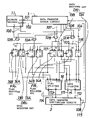
Referring to FIG. 1, there is shown a parallel
-7- ~ ~'
.. . . . . . . ...... . . .
'
21~a7~
data transfer circuit to which the present invention is
applied. The parallel data transfer circuit shown
includes a data trans~er source circuit 1, a data
transfer destination circuit 2, a decoder 11, n data
register sets DR1 to DRn each composed of a pair o~
registers 13A and 13B for an upper byte and a lower :~
byte, respectively, n corresponding flag register sets
FRl to FRn each composed o~ a pair of registers 14A and
14B for an upper byte and a lower byte corresponding to .
the registers 13A and 13B for an upper byte and a lower :~
byte of each set, respectively, a pair of OR circuits
12A and 13B for an upper byte and a lower byte
corresponding to the registers 13A and 14A ~or an upper ~ ~
byte and the registers 13B and 14B ~or a lower byte of :
each set, respectively, a data selector 15, and a flag ;~
selector 16. ~ :
In the parallel data transfer circuit, the
decoder 11 and the n OR circuits 12A and n OR circuits
12B constitute a write circuit for writing data and a
flag, and the data selector 15 and the ~lag selector 16
constitute a read circuit for reading out data and a
flag. Here, the parallel data transfer circuit can :~
transfer three kinds of data including data composed ~;~
only of an upper byte, data composed only of a lower
-8-
? 8 ~1
byte, and word data, and can transier n words in the
-~ in a single transierring operation.
It is to be noted that, while several signal
lines interconnecting the components oi the parallel
data transier circuit described above are shown in FIG.
1, each line with a slating line attached thereto
represents that the signal line is actually parallel
signal lines ior 8 bits.
When data are to be transierred, the data
transier source circuit l outputs a decoder enable
signal 101 to put the decoder 11 into an enabled ~ :
condition and then outputs to the decoder 11 a register ;~
designation signal 102 which successively designates
required ones oi the n data registers and flag
registers. Further, when upper byte data 104 and/or
lower byte data 105 are to be outputted, the data :~
transier source circuit l simultaneously outputs an : ~:
upper byte write lnstruction signal 106 and/or a lower
byte write instruction signal 107. Then, aiter .
outputting oi data ior a single transierring cycle (a -~
set oi data) is completed, the data transier circuit 1 -~
outputs a transmisslon end slgnal 108 to the data
transier destlnatlon circult 2.
The decoder 11 decodes the reglster designation
_g_
211~2~
signal 102 from the data transfer source circuit 1 and
inputs a~write permission signal 103 to the OR circuits
12A and lZB for an upper byte and a lower byte of the
set designated by the register designation signal 102. .
In the set to which the write permission signal 103 is
inputted, if an upper byte write instruction signal 106
is outputted simultaneously from the data transfer
source circuit 1, a write signal 116 is outputted from
the OR circuit 12A for an upper byte to write upper byte
data 104 from the data transfer source circuit 1 into
:: :
the data register 13A for an upper byte and place a flag
into the flag register 14A for an upper byte. On the ;.
other hand, if a lower byte write instruction signal 107
is outputted simultaneously from the data transfer
source circuit 1, a write signal 117 is outputted from
the OR circuit 12B for a lower byte to write lower byte
data 105 irom the data transfer source circuit 1 into
the data register 13B for a lower byte and place a flag
into the flag register 14B for a lower byte.
When a transmission end signal 108 is received
from the data transfer source circuit 1, the data
transfer destination circuit 2 outputs a select signal ~ :
111 to the data selector 15 and the flag selector 16. ~':
In response to the select signal 111, the data selector
--10--
2~1 ~,?~A
successively selects the n data register sets DR1 to DRn
for each of the registers 14A and 14B to read out data
and outputs the data as read data 112 to the data
transfer destination circuit 2. Meanwhile, the flag
selector 16 successively selects, in response to the
select signal 111, the n f'lag register sets FR1 to FRn
~or each of' the registers 14A and 14B to read out a flag
and outputs the flag as a ~'lag read signal 113 to the
data trans~er destination circuit 2.
The data transfer destination circuit 2 fetches
the read data 112 ftrom the data selector 15, tha$ isi
data read out from the data register selected in :
response to the select signal 111, when the flag read -~
signal 113 f'rom the flag selector 16 is "flag present"
representing presence of' a ~'lag, that is, when a flag is
held in the f'lag register selected in response to the ~;
select signal 111. On the contrary when the f'lag read
signal 113 is "~lag absent" representing absence of a
f'lag, that is, when no f'lag is held in the flag register ~ :~
selected in response to the select signal 111, the data ~ : :
trans~er destination circuit 2 ref'rains ~rom fetching
the data f'rom the data register selected in response to
the select signal 111. In other words, the data ~ '
transf'er destination circuit 2 ~etches data only ~rom
2116284
the register 13A or 13B corresponding to the register
14A or 14B in which a ~lag is held. Accordingly, no
discontinuous empty portion is produced in the data
storage area o~ the data transfer destination circuit 2.
After the data ~etching operation from all of
the register sets DRl to DRn is completed, the data
trans~er source circuit 2 outputs a reception end signal
llS to the data trans~er source circuit 1 and outputs a
reset signal 114 to the registers 14A and 14B of all of
the ~lag register sets FR1 to FRn. . -
Subsequently, an operation ~or writing only
upper byte data, another operation for writing only
lower byte data and a ~urther operation ~or writing word
data into a data register will be described.
<Writing Only of Upper Byte Data> ~-
1. A decoder enable signal 101 is outputted from
the data transfer source circuit 1 to put the decoder 11
into an enabled condition.
2. A register designation signal 102 which
designates, ior example. a ~irst register set is ~
outputted ~rom the decoder trans~er source circuit 1 to ;
the decoder 11.
3. A write permission signal io3 ~or the ~irst
set is outputted ~rom the decoder 11, and an upper byte
-12-
~' 2~16~81
write instruction signal 106 is outputted f'rom the data
transfer source clrcult 1.
4. A wrlte signal 116 is outputted from the OR
circult 12A ~or an upper byte of' the f'irst set to put
the register 13A f~or an upper byte of' the first register
set DRl and the register 14A for an upper byte of the
~irst flag register set FRl into a write enabled
condition.
5. Upper byte data 104 are outputted from the
data transf'er source circuit 1 and latched by the
register 13A ~or an upper byte o~ the first data
register set DRl, and a flag is placed into the register
14A for an upper byte of the first flag register set
FRl. ~- .
<Writing Only of Lower Byte Data>
1. A decoder enable signal 101 is outputted from
the data transfer source circuit 1 to put the decoder 11
into an enabled condition.
2. A register deslgnatlon slgnal 102 whlch ~
deslgnates, f'or example, a second reglster set is .:
outputted f'rom the decoder transf'er source circuit 1 to
the decoder 11.
3. A write permission signal io3 for the second
set is outputted f'rom the decoder 11, and an upper byte
-13-
.
211~28~
write instruction signal 106 is outputted ~rom the data
trans~er source circuit 1.
4. A write signal 117 is outputted ~rom the OR ~ -
circuit 12B ~or a lower byte of the second set to put
the register 13B for a lower byte of the second register
set DR2 and the register 14B ~or a lower byte o~ the
second ~lag register set FR2 into a write enabled
condition.
5. Lower byte data 105 are outputted from the
data trans~er source circuit 1 and latched by the
register 13B for a lower byte of the second data
register set DR2, and a ~lag is placed into the register
14B for a lower byte o~ the second ~lag register set
FR2.
<Writing of Word Data>
1. A decoder enable signal 101 is outputted ~rom ;~
the data transfer source circuit 1 to put the decoder 11
into an enabled condition.
2. A register designation signal 102 which
designates, ~or example, a third register set is
outputted ~rom the decoder trans~er source circuit 1 to
the decoder 11.
3. A write permission signal io3 ~or the third
set is outputted ~rom the decoder 11, and an upp0r byte
21~628~
write instruction signal 106 and a lower byte write
instruction signal 107 are outputted ~rom the data
trans~er source circuit 1.
4. Write signals 116 and 117 are outputted from
the OR circuit 12A ~or an upper byte and the OR circuit
12B for a lower byte o~ the third set to put the
register 13A for an upper byte and the register 13B for
a lower byte o~ the third register set DR3 and the
register 14A ~or an upper byte and the register 14B for
a lower byte o~ the third ~lag register set FR3 into a :
write enabled condition, respectlvely.
5. Upper byte data 104 are outputted from the
':
data trans~er source circuit 1 and latched by the
register 13A for an upper byte o~ the third data
register set DR3 and lower byte data 105 are latched by :
the register 13B ~or a lower byte oi the third data
register set DR3, and a ~lag is placed into each o~ the
the register 14A ~or an upper byte and the register 14B
~or a lower byte oi' the third ~lag register set FR3..
Subsequently, a reA~lng operation ior the data
registers will be described by way oi an example wherein
only upper byte data are latched ln the ~irst data
reglster set DR1 and only lower byte data are latched in
the second data register set DR2 while word data are
:,
-15-
~--" 2~1~28~
latched in the third data register set DR2 as a result
of the writing operation described above.
1. The data trans~er destination circuit 2 first
outputs, to the data selector 15 and the flag selector
16, a select signal 111 to select the register 13A ~or
an upper byte o~ the ~irst data register set DR1 and the "
register 14A ~or an upper byte o~ the ~lrst ~lag
register set FRl.
2. The data selector 15 reads out data o~ the
register 13A for an upper byte o~ the first data
register set DRl and outputs the read data 112 while the
~lag selector 16 reads out a ~lag o~ the register 14A : ~ :
~or an upper byte o~ the ~irst ~lag register set FRl and ~
outputs a ~lag read signal 113 o~ "~lag presentn. ~-
3. The data trans~er destination circuit 2
~etches the read data 112 ~rom the data selector 15
since the flag read signal 113 is "~lag presentn.
4. Then, the data trans~er destination circuit 2 '
outputs a select signal 111 to select the register 13B
~or a lower byte o~ the ~lrst data register set DRl and
the register 14B ~or a lower byte o~ the ~irst ~lag
register set FR1.
5. The data register 15 reads out data o~ the
register 14B ~or a lower byte o~ the ~irst data register
-16-
.. 21~2~i~
set DR1 and outputs the read data 112 while the flag
selector 16 reads out a flag of the register 14B for a
lower byte of the first flag register set FRl and
outputs a flag read signal 113 of "flag absent".
6. The data transfer destination circuit 2
refrains from fetching the read data 112 since the flag
read signal 113 is "~lag absent".
7. Subsequently, the data transfer destination
circuit 2 outputs a select signal 111 to select the
register 13A for an upper byte of the second data
register set DR2 and the register 14A for an upper byte
of the second flag register set FR2.
8. The data selector 15 reads out data of the
register 13A for an upper byte of the second data
register set DR2 and outputs the read data 112 while the
flag selector 16 reads out a flag of the register 14A
for an upper byte of the second flag register set FR2
and outputs a flag read signal 113 o~ ~flag absent~.
9. The data transfer destination circuit 2
refrains from ietching the read data 112 since the flag
read signal 113 is ~flag absent~.
10. Then, the data transfer destination circuit
2 outputs a select signal 111 to select the register 13B
for a lower byte o~ the second data register set DR2 and
-17-
: ~, - :~
2~162~
the register 14B for a lower byte o~ the second flag
register set FR2. :
11. The data selector 15 reads out data of the
register 13B for a lower byte of the second data
register set DR2 and outputs the read data 112 while the
flag selector 16 reads out a flag of the register 14B
for a lower byte of the second flag register set FR2 and
.outputs a flag read slgnal 113 of "flag presentn. . :
12. The data transfer destination circuit 2
fetches the read data 112 since the ~lag read signal 113
is "flag present".
13. Then, the data transfer destination circuit
2 outputs a select signal 111 to select the register 13A
for an upper byte of the third data register set DR3 and -
the register 14A for an upper byte of the third flag
register set FR3.
14. The dats selector 15 reads out data of the
register 13A for an upper byte of the third data
register set DR3 and outputs the read data 112 while the
flag selector 16 reads out a flag of the register 14A
for an upper byte of the third flag register set FR3 and
outputs a flag read signal 113 of "flag absentn.
15. The data transfer destination circuit 2
refrains from fetching the read data 112 since the flag
-18-
211~28~
read signal 113 is "~lag absent".
16. Subsequently, the data transfer destination
circuit 2 outputs a select signal 111 to select the
register 13B ~or a lower byte o~ the third data register
set DR3 and the register 14B ~or a lower byte of the
third ~lag register set FR3.
17. The data selector 15 reads out data o~ the
register 13B for a lower byte of the third data register
set DR3 and outputs the read data 112 while the flag
selector 16 reads out a flag of the register 14B for a ;
lower byte of the third flag register set FR3 and
outputs a flag read signal 113 o~ "~lag present".
18. The data trans~er destination circuit 2
fetches the read data 112 since the flag read signal 113
is "flag present".
Having now fully described the invention. it -
will be apparent to one o~ ordinary skill in the art
that many changes and modi~ications can be made thereto
without departing ~rom the spirit and scope o~ the
invention as set ~orth herein.
-19-