Note : Les descriptions sont présentées dans la langue officielle dans laquelle elles ont été soumises.
WO 93/21554 PCr/GB93/00762
1 i 7 ~ ~ B -
HIGH SPEED OPTICAL SWITCHING DEVICE INCLUDING A
CAPACITANCE STRUCTURE
The present nvenlion _eLa~es to optical switching
devlces and flnds par~ -ular appiication ln high bit rate
communlcations links.
Communlcations links wnich can carry ~igh data rates
are advantageous because thev can t-ansmit lncreased levels
of nformation and/or can ~rovlde links via a single
physical connection which servlce higher numbers of
customers. ~or instance, ~ime divlsion mult'plexed signals
on a communications link can provide a higher number of
time slots, and po~enliallv therefore service a higher
number of cuslomers, -~ne~e ~he link tself carries a higher
data rate.
In order to access the data on a communications link,
it ls necessary to do.in oad the information on the link to
a receiver. In time division multiplexing, one particular
cus~omer will requlre -. ormatlon from only one or more
- selected time slots ~o be down loaded. To do this,
switching devices may be used, the speed of switching of
~he aevice being ccmmensurate with the capability of the
link or carrying hian speed traffic. In optical
communicatlons, _. is env~saqed that data rates may be
achieved as nigh 2S ' OOGbit~s in the foreseeable future.
This might be carr ed . ,en t;me slots, providing ten
cnanneis at lOGbit~s.
.. s well as ~o~entlallv ~ncreasing the number of
customers using a communlcations link, ultra high bit rate
links in future networks may enable customers to be offered
new large bandwidth services as well as giving
teLecommunications comDanies greater flexibility in
.0 managing their ne~works. The present invention is
concerned with an imDorlant part of achieving ultra high
,~ .. .
- .~
,, . , . . _ . ,
W093/215~ ~ 2 - PCT/GB93/00762
bit rate l nks, orovlding a t~pe ~ switch capabLe of
demul'iplexlng a ~OGbit~s blt s.-eam _~om a l~OGbit/s
optical time aivislon multipiexea (OTDM) signai. An
optical clock slgnal might be used .o swltch out every
3 tenlh bit. ~ence, .o -ecover all _he aata on the link, ten
switching devices mignt be usea in ?arallel.
Switching devices are known, including switching
devices which can be controlled bv 2;1 optical input. For
instance, in ~130ps Recovery of All-optical Switching in a
.0 GaAs Multi Quantum Well Directional Coupler~' published in
Applied Physics Letters volume 58 numDer 19 on 13th May
1991 bv Li ~am Wa e~ al (Ref. (i)), a recovery time of
-
î30ps is reported ln a zero gap ci-ecllonal coupler using
multiple quantum wells. However, -t has now been
discovered in making the present lnvention that much faster
recovery times can be achieved. ~educed recovery times
provide potentiall~ faster switches, recovery time being a
limiting factor.
According to the presenl invenl on, there is provided
a semlconductor optical switching device, for use in
optical communications systems operzting at high data
- rates, the switching device comprislng an optical
waveguide, including 2 p-n ,unc~ion, provided on a
substrate, .he wavegulde havlng inpu~ and output ports for
-eceiving 2 data s~gnal 2t a _:-SI wavelenglh from a
communications link and a cont-ol slgnal at a second
wavelength, the control- slgnal operating to modify the
refractive index of at least part or the waveguide at the
first wavelength, by creating eiectrical carriers in the
region of the p-n junction, so as to change the optical
path length of the data signal in the device there being
significant capacltance across the aevice in use.
WO93~215~ ~ I 17 ~ O ~ PCT/GB93/~762
The pur-cse or ~he slgnlricanl capacitance is to sweep
car_iers ou~ o- the -egion o~~ the junction as quickly as
possible after their crea~ion by lnput or the controi
signal to the device. ~his s achieved because the
,1gnlficanl capacltance ~rovides a low impedance
-ecombination path -or ~hologenerated carriers, thus
speeding up the recoverv oî the device, and therefore its
?olEnlial switching speed.
Although the data and control signal need not both be
10 aul ded throuan the device, so that for example the data
slgnal could be guided by the waveguide while the control
slgnal is input at right angles to the waveguide and is not
gulaed by lt, Dreferably o~h the data and control signal
are guided along the wavegulde. This facilitates easy
alignment of the aevice, particularly if the data and
con~rol signal sAare Ihe same input and output port to the
waveguide.
Preferablv the significant capacitance of the device
enables in use a substantially constant potential to be
~aintained ac~oss the D-n junction. This is desirable
because :t lS this ~otentlal which provides the driving
Lorce to sweep the carriers out of the junction region.
rurthermore the significant capacitance of the device
~rererably ~acilita~es recombination of an AC component of
~5 .he electr;cal car_~ers within the device. Hence by
arranging for recombination to occur within the device the
potentially long delays encountered when allowing
recombination to occur oulside of the device, due for
example to Algh AC lmpedance of the bondwire, can be
avoided.
A suitable capacltance can be achieved by providing a
hlgner bondpad capacltance than would be used in known
devices of slmllar s.ructure. For instance, the latter may
WO93/215~ ~ PCT/GB93/~762
have a capacl~ance of the oraer of O.SpF across the
junction and a bond?ad capacitance or O.lpF cr 'ess.
Indeed, ln ~nown ~evlces .he ~m _s .o reauce Ihe
capacltance presenled. Devices according ~o the present
_ lnvention mignt, _n conlrast, presen~ a capacltance ln use
n the range of, say, ~?F to 50pF. For instance, under a
reverse bias of 5 volts, the junc~lon alone might provide
a capacitance (C~) o- 0.6pF, but _he swltching devlce as a
whole, lncluding the bondpad capacltance, might present a
capacltance (CO~t) of 23pF.
The junction can be provlded as a PIN junction,
absorptlon or lignt a~ the second (control'~ wavelength
alvlng rlse .o eiec-~on hole palrs ~-HP) as ca-rlers.
Partlcuiarly userul slgnal ana control waveiengths
lS might be i.55~m and l.3~m, these belna commonly used in
optical communlcations and sources of lisht at these
wavelengths beins readily available.
.~ switchlna device accordina _o an embodiment of the
present invention can be used as a switch by periodically
(selectively) 'ransmitting or blocking the signal
wavelength. ~his mlcht be achieved by putting the device
nto one arm or a ~ach-Zehnder :nterferometer, or by
constructing the devlce to comprlse a Fabry-Perot (FP)
cavity, or a directional coupler.
25Specific embodimen~s of the present invention wlll now
be described, wlth ~eference, bv way of example only, to
the accompanving drawings of which:
Figure 1 shows a perspective vlew of a demultiplexing
(DEMUX) chip according to an embodiment of the present
invention;
Figure ~ shows a cross sec~lon or the waveguiding
region of the chip of Flgure l;
W093/215~ ~ 7 S ~ 6 PCT/GB93/~762
~igure 3 shows a circult model oî the DEMUX chip of
Figure l;
Figure ~ snows an experimental arrangement for
investigatlng operat_on of the DEMUX chip of Figure l;
~igure snows experlmental results obtained with the
experimental ar_angement or Figure 4, in particular the
measured -atlo of _he optlcally modulated signal to an
optical modula~i..g slgnal; and
Figure 6 shows an alternative embodiment of a DEMUX
chip for use ln the present invention.
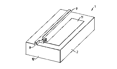
Referring to r igures l and 2, an embodiment of the
present invention comprlses a PIN waveguide device
structure l, deslgnea ~o demultiplex a lOGbit/s bit stream
'rom a 100Gbit/s OTDM signai at l.55~m wavelength. Such a
switching devlce might then be used as a DEMUX chip with an
optical clock signal of '.3~m wavelength, the clock signal
being used to switch out, 'or instance, every tenth bit of
the lOOGbit~s slgnai.
The PIN waveguide device structure l is grown by MOVPE
growth techniques, these being known and not consequently
further describea herein. mhe structure is based on a Sn
doped InP substra~e 2. The layers grown onto the substrate
are as follows, n order:
. ~ ~
i) 2xlO'~cm~ â coped n~ InP layer 3 index matched
.o the substratei
ii) 3xlO;7~m' S doped n InP buffer layer 4;
(iii) 0.30~m quaternary (Q) l.44 layer 5;
(iv) 0.l8~m undoped T nP layer 6;
(v) 8.3x lOI7cm~ Zn doped p+ InP layer 7.
Referrina partlcularly to Figure l, input and output
ports 8, ~ are provlded as facets at either end of the
waveguiding structure. Absorption of l.3~m light in the
Ql.44 guidin~ layer 5 gives rise to EHPs and an associated
WO93J215~ 2t ~ u~ _ 6 - PCT/GB93/00762
change in ~he -errac~ e lndex (~n) of this layer 5 for
:.55~m iight. ~he ~-ansmltted intensity at 1.55~m can then
be optlcaily cont_olied by putting .he aevlce into a
Mach-Zehnder nter-erometer ~ype o~ arrangement or by
_elying on a FaDry-?erot cavity. Ultr~ high speed
operation is made 20sslble by using the new approach of on
chip recombination o- swept EHPs, discussed in further
detail below. The c.-ange ln -efract ve index, ~n, lS due
.o effects of bana -~ling, band gap shrinkage and free
carrier absorption, _ scussed in the followlng two papers:
Ref (ii) "Carr:er-Induced Change in Refractive Index
of Ina, GaAs and InGaAsP" IEEE Journal of
Quan.um _lectronlcs, volume 26 number
Janua-. 1990 by Bennett et al
~ef (ii ) "Ir.P/GaInAsP Guided-wave Phase Modulators
basea on Car-ler-induced Effects, Theory and
Exper:mentl' Journal of Lightwave Technology
voiume 0 numDer 1 January lg92 by Vinchant
et =i.
~ractical detalls of operatlon of the embodiment of
the present invent on shown ~n the Flgures are as follows:
~ulse Enercv ~eaulred ~or Switching:
Besides havlng .he polential -or lntegratlon Wl th
other devices ~pera~ing in .he ;.3~m or 1.55~m
telecommunicat1ons wlndows, uslng InGaAsP lattice
matched to InP ~s advantageous in that its bandgap can
be chosen such .hat ~n will be maximised for a given
wavelength. ~he bandgap wavelength of 1.44~m was
selected to glve a large value of ~n due to the close
proximit~ OI ~his wavelength to 1.55~m, whilst
mainlainlng ~n acceptably small absorption
coeff_clent. ~or this choice of bandgap the dominant
WO93/215~ ~ 1 7 S O ~ PCT/GBg3/~762
., -- 7
contr~bullon .c ~n ;s expecleà to be bandfilling, with
the bana-aap ~ n~age and 'ree carrier absorption
?rocesses belr,~ smailer and of opposite polaritles to
one anolner Isee Ref. (i~) above).From consideration
_ of the banaf_: ng effect aione a proportlonality
constant rela.:ns ~n IO the free carrier density of
appro~imately -.Y102~cm~ is theoretically predicted
(see Ref. ~lii; aDove)~ A high finesse FP cavlty is
then used .~ convert this phase modulation into
intensity moaulation of 1.55~m light. This was
accomplished -y applying facet coatings at the
input~oulput ?orls 8, 9 of reflectivity 84~ at 1.55~m
and 8% a. l._~m. ~Jhen ~hese coatlngs were applied to
a device of length 540~m a 9.ldB contrast ratlo was
achieved by tuning through the FP spectrum. The
estimated contrast ratio obtained when lpJ of 1.3~m
light is coupled into the device is calculated to be
6.ldB using ~he proportionality constant above and
standard F~ theory (Ref. (iv): "Simple and Accurate-
Loss Measuremen- Cor Semiconductor Optical Waveguides"
Electronlcs Lel.ers Vol. 1 pp 581-583 by R G Walker).
~evlce Sw1tch~ S~eea:
~n init;ai invesliqat on of the free carrier induced
~n uslna unaopea waveguides indicated that free
carriers have 2 iifetime of approximately 8ns for this
material system. In the working device this free
carrier lifetime needs to be reduced to <10ps in order
to facilitate 100Gbits ~ operation. For practical
purposes the .urn-on tlme can be considered to be
0 lnstantaneous compared to the switch-down time. By
~ the appilcatlon of sufficlent reverse bias between the
p-contac. (bonapad) 'l and n-contact (metallized
~ ... . . _ . .
WO93~215~ ~ PCT/GB93/~762
~ ~ 8 -
substrate) , ~n electric field can be established
across the depleted guiding layer 5, ~ resultin~ in
removal of E~P at a rate determined bv their trans
times out o, _his layer. If we assume that .he
saturatea car-ler velocities of eiectrons ana holes
have the same ~aiue as in InGaAs 7xlO6cms1 and
5xlO6cms -espectlvely, then all carriers will be
removed -rom ~he depletion region in <lOps with the
mean carrier transit time being 4.4ps (Ref. (v):
"GaInAsP Alloy Semiconductors" by T P Pearsall,
published bv Wiiey l982).
The idea cf reverse biasing an optical switch to
sweep carriers out of its guiding region has been
reported before (see Ref. (i) above). By reverse
biasing an MQW structure carriers were swept out of
the guiding region to bring the recovery time down to
130ps. However the device structure reported here is
significantiy different in the following two ways.
Firstly we are employing a bulk semiconductor guiding
layer. ~s a consequence of this generated carriers
don't have ta tunnel through barriers and hence are
not slowed down on their way out of the guiding layer.
The second and more fundamental divergence relates tO
the current ?ulse that is initiated by the removal of
EHP from the depletion region. '~hen the carriers are
swept out at .heir saturated carrier velocities this
current pulse will be of several hundred mA in
magnitude. At impedances above a few ohms, it can be
seen that ~otentials of several volts could be
generated across the external circuit in opposition to
the bias voltage. The DEMUX chip and bias circuit can
be represented by the circuit element model lO shown
in Figure 3. When under a reverse bias of 5V the pin
-
W093/215~ ,~11 7 g 0 6 PCT/GB93/~762
. _ 9 _
,unc-:on has _ 'eakage current of '70pA and a
capacitance Cd=~.6pF. The resistance 13 associated
wlth the path ~~m the metallizea ridge to the bondpad
;1 is approxima~ely ~=1.6~. The large area bondpad
1;, fabr~ca~ea _sina a O.l~m SiNx dielectric layer,
has a capacitance a~ -5V of Celt=23pF. When the 1.3~m
clock pulse has a repe~ition rate of lOG~z the current
generated wil' ~onsist or a DC component in addition
to AC componen~s going up to in excess of lOOGHz in
lOGHz steps. ~rMUX chips were bonded to laser headers
to ,acilitate ~he application of a bias voltage.
There will inevltably be a bondwire inductance L, 14,
of severzi nH ac.ing ~n serles with various external
reslstances R. ~s long as R is less than a few ohms
the DC componer~ o_ .he current will recombine off
chip witAout d-opping the junction potent al by a
significant amount. ~he case is different for the AC
componen~s due .o the large impedance of the bondwire
at ~hese 're~uencies. This necessitates on chi~
recombination~hich s made possible by the high value
Ce~t. For the values given above assuming that any
inductance ln series R is of negligible size,
lOOGbits opera~ion is predicted for low reverse
voltages.
~he ldea o- increasing the bondpad capacitance to
improve Aigh speed perrormance is directly opposite to
the approach required for photodetectors and electro-
optic modulators, and is what sets this device apart
from previous work.
~x~erimen~:
Using the lay-o~ shown in Figure 4, a CW beam from a
1. 56~m DFB l_ was wavelength tuned so that the
WO93/215~ PCT/GB93/00762
k ~ 10
cl~
transmlt_ed ~ ode f-om the reverse blased DEMUX chlp
1 was rouahly 2. a 30int in lls F~ spect-um where the
change ,n ~ansmltted intens;ty -or small ~n was
optlnised. This beam was then modulatea i~ the DEMUX
c chip 1 by ampiif:ea 1.3~m puises of approxlmatel~ 25ps
FWHM duralion oDtained by galn switching a DFB 16 at
a lGHz repetition rate. The signal was detected by a
nigh speed ?in 3notodetector 17, amplified, and then
displayea on an r- spectrum analyser 18. At each
'0 frequency the sicnal level was calibrated aaalnst the
1.3~m sianal a~ _hat frequency. The spectrum of the
1.3~m puise was observed by connecting the output of
the WDM coupler 19 to the high speed pln 17.
Measuremenls were conducted in the -requency domain
because -n Ihe .ime domain using this source the
response would be dominated by the spectral components
outside the range of interest.
Results and discussion:
With the DEMUX Chlp 1 under a lV reverse bias optical
modulation was cbserved at freauencles up to 20GHz.
Using =his ~easurement approach there was a
restriction imposed by tne spectrum of the 1.3~m pulse
which falls off at around 20GHz. The measured ratio
of the 1.56~m slanal to the 1.3~m signal _s displayed
in Figure 5. -t can be seen that in the rrequency
range of _nterest (ilOGHz) the ratio of the modulated
to modulating signal remains approximately constant.
Since the impedance of the current recombination path
varies with f-eauency, this suggests that over this
freauency ranae ehe lmpedance ls sufficiently low so
as not to slow the free carriers down from their
- saturated carrier veiocities. The observed optical
WO93/21554 ~1 1 7 ~ O ~ PCT/GB93/00762
~odulation c- the 1.56~m slgnal is larger by a factor
of ~ than -ha~ ,-eoretlcally predicted from the level
of the ~ m slgnal lf a mean carrier lifetime of
4.4ps ana a ~n ~ropor~onality constant of 5xlO2~cm-
_ are assumea. -eiow lOGHz the ratio of modulated to
modula~ing slcnai increases with decreasing frequency.
This has ye~ =o be accurately modelled, but it is
believed to be -elated to the higher recombination
path elect~ical ~mpedances at these frequencies. If
iO the impedance or .he path between Cd and Cext could be
made to be negliglble, then this design could function
as an aii optlcal wavelength converter besides its
envlsaged rcle as a demuitlplexer.
3EMUX _hlps using the novel swept carrier
technique coula be used to demuliplex an ultra fast
bitstream ~y empioying either the high finesse FP
cavity .echnlque or the more familiar Mach-Zehnder
approach. :~en .he FP cavity method is employed the
amount of er.ergy requlred in the switching pulse is
less. However the iinewidth of the lOOGbitsl
bitstream wlll be at least 0.8nm which is not
negligibly small ~n comparison with the spacing of
adjacent maxlma c the DEMUX FP spectrum. This fact
when taken lnto consideration alongside the
requiremen~ _o ~eep the mean photon lifetime in the
cavity down -o values less than the bit period implies
that there s llttle benefit to be accrued from
reducing the device length or absorption loss to
values below those reported here.
Referrlng to rigure 6, an alternative form of DEMUX
chip for use ln embodiments of the present invention
comprises a rlcge oO flanked by a double channel
arrangement 61, c2. ~he upper surface of the chip la is
W093/21554 PCT/GB93/~762
~ 12 -
metallized 63 on .op of a thin (lOOOA) nitride iayer.
Electrical contac. s made to the ridge region only. The
layer structure :s otherwlse the same as that shown in
Figure 1.
The double channel structure may be used wlth a
variety of channel e~ch depths, for instance, or other
variations. An example is that etching could stop part of
the way through, ~r above, the guiding layer 5.
The form of DEMUX chip shown in Figure 6 has a
particularly simple s~ructure and is thus easily fabricated
with high yield.