Note : Les descriptions sont présentées dans la langue officielle dans laquelle elles ont été soumises.
2~.1~5~7
~O 93/09414 -1- PCT/US92/09537
THIri FILM PYROELECTRIC IMAGING ARRAY
This invention relates to a thin film pyroelectric
imaging array and, more particularly, to a thin film
pyroelectric imaging array constructed from coplanar
S electrodes on a silicon substrate utilizing a platinum
electrode suspended by four bridge supports over an
evacuated silicon cavity.
BACKGROUND OF THE INVENTION
Integrated pyroelectric infrared sensors using PbTi03
thin films are well-known in the art. Prior art radiation
sensing arrays have been constructed to sense infrared
radiation using a PbTi03 thin film on a Pt-coated mica,
silicon crystal. or silicon membrane where the thin film was
deposited by RF sputtering. Some prior art methods have
employed a linear array sensor having up to 16 elements.
Operating parameters of these devices have been
characterized and are well known.
PbTi03 has been of interest due to its ability to
operate at room temperature. Room temperature operational
infrared sensors can be used for such applications as
remote sensing, biomedical tomography and gas detection.
Pyroelectric infrared sensors enjoy some unique advantages
over other sensors such as photon sensors. Photon sensors
operating in the mid to far infrared region suffer from
very low operating temperature requirements which do not
provide the advantage of pyroelectric detectors which can
be operated at room temperature and operate well throughout
the infrared region. Pyroelectric detectors have small
wavelength dependence over a wide infrared range and enjoy
a fast responses time. PbTi03 shows excellent pyroelectric
characteristic:a because of its large pyroelectric
coefficient and high Curie temperature.
Prior art pyroelectric detectors have been constructed
from materials such as PbTi03 ceramics and LiTa03 single
° 35 crystals. The prior art employed thin film construction
techniques to manufacture planar devices. Figure lA shows
a PbTi03 thin film device constructed with RF sputtering.
The device has. been fabricated as an infrared sensitive
linear array which has a structure of PbTi03 thin film on a
WO 93/09414 PCT/US92/09537
2
silicon substrate.
The structures in Figure lA have been constructed of
a thin film of PbTi03 110, a silicon membrane 160, a silicon
dioxide layer 150 and an aluminum conductor or Au-black
conductor 120. Substrates were created also from a mica
sheet 140 with a thickness of 20-50 microns or a silicon
single crystal 140. To thin out the silicon membrane, the
silicon was preferentially etched into a rectangular thin
layer of about 5-20 microns thickness. Platinum/ titanium
electrodes 130 with 16 elements were formed on a substrate.
The PbTi03 110 thin film has a thickness of about 2.1
microns which is deposited by RF sputtering. An aluminum
or Au-black layer 120 is formed as an infrared absorbing
electrode. The array sensor was electrically poled before
measuring the infrared response by applying a high electric
field to the PbTi03 110 thin film at high temperature. This
PbTi03 pyroelectric infrared sensor is described in more
detail in a publication of the faculty of Engineering
Science, Osaka University, Japan, entitled "Integrated
Pyroelectric Infrared Sensor Using PbTi03 Thin Film",
Masanori Okuyama, Hiroyuki Seto, Motohiro Kojima, Yasushi
Matsui and Yoshihiro Hamakawa, Proceedings of the 14th
Conference (1982 International) on Solid State Devices,
Tokyo, 1982; Japanese Journal of Applied Physics, Volume 22
(1983) Supplement 22-1, pp. 465-468.
Figure 2 shows an equivalent circuit 200 of the array
sensor of Okuyama, et al. The photodetection element of
the array is modeled as a connection of a current source in
parallel with a capacitor 210. A pyroelectric current
induced under illumination fills the capacitor 210 with
charge proportional to the integral of current over time.
The charge is then switched through a connecting FET 220 by
applying a gate pulse with a sample interval. The circuit
200 is then connected to a current amplifier for sampling.
Current sampling effectively resets the sensor which is
required by each sampling period.
An alternate integrated pyroelectric infrared sensor
WU 93/09414 2 ~ g ~ PCT/US92/09537
3
is described in an article from the faculty of Engineering
Science at Osaka University, Japan, dated December 17,
w 1984, found in the International Journal of Infrared and
Millimeter Waves, Volume 6, No. 1, 1985 entitled "Si
Monolithic Integrated Pyroelectric Infrared Sensor Made of
PbTi03 Thin Film" by Masanori Okuyama, Kohzo Ohtani, Toshi-
yukiueda, and Yoshihiro Hamakawa. In this sensor, the
PbTi03 thin film is sputtered onto a silicon wafer.
Referring to Figure 1B, a three dimensional drawing of
the method of Okuyama, et al. 1985 is shown. In Okuyama,
et al. 1985, the PbTi03 device is now constructed as an
interdigitized sensor built out of silicon cantilevers or
silicon bridges. The approach described in the 1985
Okuyama,et al. paper suffers from similar thermal problems
of the device in the Okuyama, et al. 1984 paper. Such
silicon structures whether solid substrate bridges or
cantilevers are also poorly thermally isolated.
Therefore, it is one motivation of this invention to
provide a nove:L PbTi03 based pyroelectric sensor that is
more sensitive to incoming infrared radiation by providing
a means of more effective thermal isolation.
The invention advantageously utilizes micromachining
techniques. 'techniques of dynamic micromechanics on
silicon have been well-known in the art. A good review of
dynamic micromachining techniques can be found in an
article by Curt: E. Peterson in the IEEE Transactions on
Electronic Devices, Vol. ED-25, No. 10, October 1978, Page
1241-1250. Silicon based dynamic micromechanics has been
used for a number of applications including oil film
projection systems, light valves, thin metal-coated SiOZ
membranes, pie::oresistive strain and pressure sensors,
deflectable plated-metal cantilever beams, frequency
filters, gas chromatography, and hydraulic valves utilizing
silicon membranes among others. Micromechanical devices
have been constructed of a thin insulated membrane attached
to a silicon substrate at one end and suspended over a pit
in the silicon. The pit is constructed by silicon etching
CA 02118597 2000-06-29
64159-1282
4
from under the deposited insulating film using a preferential
etching procedure.
Summary of the Invention
The invention provides an imaging array comprised of
a thin film pyroelectric array of one or two dimensions. In
one example, an array of silicon oxide or silicon nitride
microbridges is prepared with a film of pyroelectric material
such as PbTi03 deposited on the silicon oxide or silicon
nitride. Modulated infrared radiation incident upon the PbTi03
causes the generation of a time dependent electric signal in
the pyroelectric material, whose radiant amplitude, which
varies from pixel to pixel, and reproduces the radiant power
distribution incident upon the array.
In accordance with the present invention, there is
provided a radiation sensor having a plurality of radiation
sensing pixels arranged in an array of pixels having an
individual row and column address for each pixel and connected
to be read out by said individual address, wherein the
radiation sensing pixel comprises: (a) a substrate having
opposing flat surfaces wherein one surface has a cavity; (b) a
microbridge suspended over the cavity comprised of a material
selected from the group consisting of silicon oxide and silicon
nitride, wherein the microbridge includes a plurality of
support legs; (c) a first conductive thin film electrode
deposited on one of the legs covering substantially half the
surface of the microbridge; (d) a second conductive thin film
electrode deposited on the opposing leg and substantially
covering the remaining portion of the microbridge in such a
manner as to allow a gap to exist between the first and second
electrodes; (e) a thin film of pyroelectric material deposited
on, and substantially covering, the surface of the first and
CA 02118597 2000-06-29
64159-1282
4a
second electrodes; and (f) a thin film conductor deposited on
the surface of the pyroelectric material.
It is an object of the invention to provide a
pyroelectric array built on a thin layer of PbTi03 deposited on
a silicon oxide or silicon nitride microbridge structure.
It is another object of the invention to provide a
pyroelectric array with high responsivity.
It is a further object of the invention to provide an
infrared imaging system that does not depend on cryogenic
cooling.
It is yet a further object of the invention to
provide a pyroelectric imaging array that combines the thermal
isolation of a silicon oxide or silicon nitride microbridge
with the detection advantages of a pyroelectric material.
It is yet a further object of the invention to
provide a pyroelectric array that does not require a bias.
It is yet a further object of the invention to
provide a pyroelectric array that reduces self heating due to
power losses.
It is a further object of the invention to provide a
pyroelectric imaging array that minimizes 1/F power noise where
F is frequency.
It is still a further object of the invention to
provide a pyroelectric imaging array that has a reduced
WO 93/09414 ~ ~ ~ PCT/US92/09537
power requirement useful for battery powered man-portable
thermal imaging viewers.
It is yet a further object of the invention to provide
a pyroelectric imaging array that does not need background
5 subtraction circuitry.
It is yet a further object of the invention to provide
a pyroelectric imaging array where the electrical RC
constant can be made compatible with the frame time
requirement.
Other objects, features and advantages of the present
invention will become apparent to those skilled in the art
though the Description of the Preferred Embodiment, Claims,
and drawings herein wherein like numerals refer to like
elements.
HRIEF DESCRIPTION OF THE DRAWINGS
To illustrate the invention, a preferred embodiment of
this invention will be described herein with reference to
the accompanying drawings. The preferred embodiment
concerns an imaging array composed of a thin film
pyroelectric array of one or two dimensions.
Figure lA shows a top and side view of the prior art
sensor.
Figure 1H. shows an isometric view of a prior art
pyroelectric sensor.
Figure 2 :shows an equivalent circuit of the prior art
sensor.
Figure 3 shows an output current verses sample
interval response curve sets of a prior art sensor.
Figure 4A shows a top down view of one embodiment of
the invention.
Figure 4E~ shows a side view of the overlapping
electrode of one embodiment of the invention.
Figure 4C shows an isometric view of one example of
the invention using overlapping electrodes.
Figure 5A shows a top down view of an adjacent
electrode embodiment of the invention.
Figure 5B shows a side view of the adjacent electrode
WO 93/09414 PCT/US92/09537
2~~~~97
6
embodiment of the invention.
Figure 5C shows an isometric view of the adjacent
electrode embodiment of the invention.
Figure 6 shows schematically a pyroelectric imaging
array architecture employed in one example of the
invention.
Figure 7 shows a more detailed schematic of a single
pixel used in the architecture of Figure 6.
DESCRIPTION OF THE PREFERRED EMBODIMENT
To fully describe the preferred embodiment of the
invention the theoretical performance of a pyroelectric
detector will be explained. After careful review of the
theory and operation of a pyroelectric detector, it will be
shown that the invention markedly enhances the
responsivity, noise immunity and detectivity of a
pyroelectric imaging sensor.
Theoretical Performance of a Pyroelectric Detector
Respons ivitY
The responsivity R of a pyroelectric detector can be
described by:
R=(~wpAr/G) (1+w'tE) -m2 (1+w_iT) -m:
Here ~ is the fraction of incident radiant power absorbed
by the sensitive element, w is the angular frequency, p
is the pyroelectric coefficient, A is the area of the
sensitive element, r is the parallel resistance, req is the
sensitive element resistance, r~ is the resistance of the
input to the readout electronics, G is the appropriate
thermal conductance, zE is the electrical time constant,
and zT is the thermal time constant. The sensitive
WO 93/09414 ~ ~ ~ ~ PCT/US92/09537
7
element is the composite structure of the pyroelectric thin
layer on its silicon oxide or silicon nitride microbridge.
The electrical time constant zE' is given by the
product of the parallel resistance and the parallel
capacitance of the sensitive element and readout
electronics. It will be assumed that the capacitance of
the sensitivE~ element CSE determines the overall
capacitance. Thus the effective electrical time constant iE
is
t e=rCse ( 2 )
The value of CS;E is given by
C =e~eoA/d ( 3 )
se
where e~ is the dielectric constant of the sensitive
element, eo is the permittivity of free space, and d is
the thickness of the sensitive element.
The thermal time constant iT is given by
t T=H/ G ( 4 )
where H is the thermal mass (heat capacity) of the
sensitive element and G is the thermal conductance between
the sensitive element and its surroundings. Thus
H = c'Ad (5)
where c' is the heat capacity per unit volume of the
sensitive element.
Noise
Consider now the sources of noise. These include
Johnson noise, temperature fluctuation noise, background
fluctuation noise, and amplifier noise. Since the detector
is operated unbiased, there will be no 1/f noise. It is
WO 93/09414 PCT/US92/09537
2I1~5~'~
8
assumed that 1/f noise from the readout electronics is
negligible. The Johnson noise voltage VN,s
in the equivalent resistance r~ is given by
VH,sE= I4kTr~wtEtanb (1+w'tE) -'] 1/2
where k is Boltzmann's constant, T is the absolute
temperature, B is the electrical bandwidth, and tan8 is
the loss tangent of the pyroelectric element, defined as
tans= (wreaCsE) 1= (wPeqe~eo) -1= (wze) -1 (7)
where peQ is the equivalent resistivity associate with req.
Thus the Johnson noise in the sensitive element can
also be expressed as
vrv.sE= I4kTra~B(1+w2zE) -i] i/~ (g)
In quadrature with the Johnson noise in the sensitive
element is Johnson noise in the input resistance, given by
vN.rx= (4kTrLB) 1/' (9)
In pyroelectric materials there are two contributions to
the loss tangent. One is the intrinsic loss resistance of
the material. The other is due to "electro-thermal
coupling." Prior art works have shown that for
pyroelectric materials the thermal and electrical
properties are uniquely interrelated. The loss tangent of
pyroelectric materials due to electro-thermal coupling is
tanb=kTwzT(1+w'zT) -1 (1D)
where kT, the electro-thermal coupling factor, is given by
kT= (PZT(c~e~eo) -1] (1~
WO 93/09414 2 ~ ~ ~ ~ ~ PCT/US92/09537
9
The contribution to Johnson noise arising from electro-
thermal coupling is thus given by
4kT2rz PZw2A2B
Vnr, su, err= C e° ) i ~ z (~)
G(1+w2tE) (1+w'tT)
or
m=
4kG8(1+wZtT)
Vnr, s~~, c~r= w zA z p 2 ( 1 w'- t z )
+ E
The contribution from electro-thermal coupling manifests
itself as temperature fluctuation noise, arising from
either conducaion to the substrate or radiative
interchange. Thus it is not necessary to postulate
temperature fluctuation noise as a separate mechanism; in
pyroelectric materials it is a manifestation of Johnson
noise due to el.ectro-thermal coupling.
Detectivit~
The value of the detectivity, represented by D*, is
obtained from
D*= (AB) 1~'R ( VN) -1 (14)
Under tho:ae conditions in which the intrinsic loss
resistance of the sensitive element is the dominant source
of Johnson noise,
the value of D*, obtained by combining equations (1), (8)
and (14) is
'~pAw (AZ'eo(kT) -1 (1+W~tT) -1) i/_
D*=-
2G
Under those conditions in which electro-thermal
coupling determines the loss, and the Johnson noise
associated with it is dominant, the value of D*, obtained
WO 93/09414 PCT/US92/09537
2~I$5~7
by combining equations (1), (12), (14) is
D*~.= [~1'-A (4kT=G) '1] 1,_
The value of D* given by equation (16) is the temperature
fluctuation noise limit. Under those conditions in which
5 the dominant conduction loss is radiative interchange, the
value of G is given by
GRI=4Ari a T' (f7)
where a is the Stephan-Boltzmann constant. In this case
D*RI- [~1 (l6okT5) '1] i/z (18)
10 which is the well-known expression for the background
limited D* of thermal detectors. It is set by temperature
fluctuation noise arising from radiative interchange
between the sensitive element and the background. Its
value at room temperature for r)=1 is 1.8x10'° cm
Hz~~2/Watt.
In practice, the Johnson noise associated with the
input resistance of the electronics must be included in the
total noise.
Therefore, the total noise, consisting of contributions
from electro-thermal coupling, the intrinsic loss
resistance, and the input resistance is given by
,m_
4kTre~ + 4kGB(1+w2iT) +4kTI B~
(1+w2iE) w'A'P' (1+w2TE) L ~)
J
In this case, D* is determined from equations (1), (14),
and (19).
Properties of PbTiO~
PbTi03 has been investigated for use as a pyroelectric
material both in bulk crystal and thin film forms.
Representative values for a 2um thick sputtered film are as
WO 93/09414 ~ ~ ~ PCT/US92/09537
11
follows:
TABLE 1
Properties of PbTi03
p 6x10'8 Coul/cm2 deg K
e~f..l. 200
cue. 3.2 Joules/cm3 deg K
T~ 470 deg C
Here T~ is the Curie temperature.
Other pyroelectric materials are suitable for use in
the apparatus ~of the invention, examples include lithium
niobate (LiNb03), lithium tantalate (LiTao3), barium
titanate (BaTi~03), triglycine sulfate (TGS), zinc oxide
(Zn0) and lead zirconium titanate (PZT).
Referring now to Figure 4A, a schematic view of the
sensor of the invention is shown from the one side of a
silicon wafer. The invention is fabricated from a wafer of
single crystal silicon upon which various processes deposit
functional elements. Special features, such as thermal
isolation cavities are formed by preferential etching or
equivalent processes. Figure 4A shows the top view of a
pyroelectric pixel indicating the configuration of the
current carrying legs 20 and 30. Figure 4A shows the
silicon substrate 10 which surrounds the pyroelectric pixel
and also provides the supporting material for the pixel
itself.
A cross section of Figure 4A is shown by Figure 4B.
The silicon substrate 10 is etched away under a silicon
oxide or sili~~on nitride to form a 45 on which the
pyroelectric material has been previously deposited. The
radiation sensing pixel is formed from a sandwich of
conducting material and PbTi03 supported by the structural,
nonconducting legs of the microbridge 45. The conducting
material of the current carrying legs 30 and 20 is isolated
WO 93/09414 PCf/US92/09537
~.~~g~9~'
12
from the silicon substrate by a layer of silicon dioxide or
silicon nitride, SiOz, or silicon nitride, Si3N~. The
current carrying leg 30 forms one plate of the capacitor
and can be seen in Figure 4A as the large diamond in the
center. The conducting material of the opposite current
carrying leg 20 forms the other plate of the capacitor,
part of which is shown on the left side and part of which
is obscured by the diamond in the center. The cavity 70
beneath the pyroelectric pixel physically isolates the
pixel from the silicon substrate.
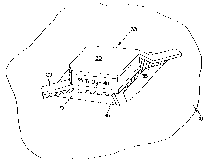
Figure 4C shows an isometric view of one example of
the pyroelectric pixel 33 of the invention. The opposing
electrode configuration of the invention is illustrated
wherein the PbTi03 is sandwiched between the Pt electrode
pair. The thermally isolated microbridge can be seen
suspended over cavity 70. Current carrying legs 20 and 30
can be clearly viewed as forming a capacitive structure
with the PbTi03 40. The support legs 45 are providing
mechanical support as well as affording good thermal
isolation from the silicon substrate 10. Absorbed infrared
radiation is sensed by the PbTi03, the voltage difference
across the leads 30 and 20 being proportional to the amount
of absorbed radiation.
Referring now to Figure 5A, the schematic view of
the sensor is shown from one side of a silicon substrate.
Figure 5A shows an alternative top view of the pyroelectric
pixel indicating the configuration of the current carrying
legs 20 and 30. Figure 5A differs from Figure 4A in that
the current carrying electrode 30 is no longer electrically
connected to the first plate of the capacitor numbered at
25 in Figure 5A.
Figure 5B shows a cross section of a pyroelectric
detector forming an alternate embodiment pyroelectric
pixel. The PbTi03 40 is suspended by a silicon dioxide or
silicon nitride microbridge over cavity 70. The PbTi03
sensing element is sandwiched between the current carrying
legs 20 and 30 and the free plate 25. The free plate 25,
WO 93/09414 ~ ~ ~ ~ ~ ~ 7 PCT/US92/09537
13
along with the adjacent electrodes 20 and 30, enable a more
easily fabricated structure. The embodiment of the
invention also provides an effective means of thermally
isolating the PbTi03 sensing element from the silicon
substrate.
Figure 5C shows an isometric view of the pyroelectric
imaging
sensor of this alternate embodiment of the invention. The
isolated sensor can be seen suspended over cavity 70.
l0 Current carrying legs 20 and 30 can be clearly seen, as in
the alternate embodiment, as forming a sandwich with the
PbTi03 40 and an isolated conducting layer forming an
alternate capacitor plate 25. The supporting legs 45 are
providing mechanical support as well s providing good
thermal isolation by separating the PbTi03 sensor from the
silicon substrate. Absorbed radiation is sensed by the
PbTi03 by a voltage difference across leads 30 and 20
proportional to incident radiation.
Now referring to Figure 6 which shows the arrangement
of rows and columns of the PbTi03 readout electronics. Each
pixel 701 is represented by a square. The array is arranged
in an M by N row and column fashion. A mechanical shutter
704 move in the' direction of motion indicated by arrow 706.
The mechanical shutter 704 selectively shades each of the
N rows of M columns as it progresses along the array. Thus
pixels 701 area prevented from sensing incident radiation
when covered bay the shutter 704. The data output pads 708
are used to send information from the array to the system
using the arra:Y. Row select line 710 selects one of the N
rows.
Now referring to Figure 7 which shows the details
within each pixel 701, enclosed by the dotted line. The
PbTi03 pyroelectric detector is represented by the 2pF
capacitor 801. The remaining devices are deposited or
constructed either underneath or alongside in the silicon
10. This includes 3 FET's and a 0.1 pF capacitor. The 0.1
pF capacitor 803 can also be made of PbTi03 in which case it
211~~'~7
- 14 -
is shielded from any incident thermal radiation. _Tn use
each p=xel 701 is scanned sequentially from left to right
in a selected row. Then from left to rigrt in the
' adjacent row immediately below and so on. 'she shutter is
synchronized to the vertical scanning speed.
In one example e~cdiment of the =nvention t a FE='s
of the apparatus of the invention era 25 microns wi3e and
Sc: microns lone;. Those skil led in t'~e a~ will reccgr.i ze
that it is des~:rable tc have the electronics benea~-..i-. the
tG microbridge stzwctsre in which case the use of a
"sacrificial laiyer" is required in processing the a~rav.
In an altarnat::ve eabodiment of the invention, t:~e
e~.ectronics can be in the silicon substrate alongside the
micrcbridge. ~:f t_he electronics are constructed a=cngside
15 the micrflbridgE: the area of each pixel is then.
apnrcximately doubled, however the sensitive parT cr. the
microbri3ge remains the same.
T2,.is invention has been described herein in
considerable d~aai. in order to comply with the Fatent
zo Statstes and to provide t hose skilled in t.'?e art wi th tZe
information needed to apply 'he novel principles az.~~. to
construct and use such specialized components as are
required. However, it is to he understood that the
invention can be carried out by specifically differ=_:~
2~ equipment and devices, and that various modificaz~.crs,
both as to the equipment details and operating procedures,
can be accomplished without departing from the scope of
the invention :itsel f .
Exaaples of previous infrared detectors in this area
3c) can be 'vuad in G10 91/16607 entitled "Semiconductor Film
3olameter Ther~aal Infrared Detector" and latent Abstracts
OZ JaDa~, vol. 11, no. 22 (P-538) 21st January 1987 8 JP-A-
61195318 (Mats»shita Electric Ind Company Ltd) 29th August
1986.
3~ What is claimed is
$~it'3~T~ ~ ~' i ~ ~~"~1~~~