Note : Les descriptions sont présentées dans la langue officielle dans laquelle elles ont été soumises.
91-SM6-~60~s
6~~11~61~
12-7S7
~VAFElt REIL:~SE 1~E~~fD ~,ND ~'~TIJS
S
Field of the Invention
'The present invention concerns an electrostatic clamp for.,halding a
semiconductor wafer against a wafer support and more particularly to a method
and apparatus for controlling operation of such a clamp.
1S lBack~round Art
A.J.S. T'atent hlo, 5,103,367, entitled .Electr~ost~rtic ~'huck Tlsing~l.C.
Field
~cztation relates to a ra~echar~ism for holding semiconductor wafers in
c~nntact with
a support during treatment of the wafers. The electrostatic chuck has three
electrodes where two electrodes define a substantially planar surface and are
embedded within a thin dielectric elm. These two electrodes are excited by a
low-
frequency (approxiagately 200 hertz) A.~, supply to produce sign wave gelds of
controlled amplitude and phase. T°he third electrode accesses a shield
electrode
that serves as a reference point for the other two electrodes. 13y controlled
rates
of voltage application and rezraoval, low-voltage gradients are obtained on
the
2~ wafer support. ~?nis results in no retentive forces between the dielectric
medium
and the v~afer. , A low alternating current amplitude excitation of the chuck
enables capacitative current sensing of the relative positions of the wafers
and the
dielectric hlm enabling simple control of voltage application to the
electrodes.
A common problem associated with electrostatic clamping is that the wafer
may not release from the clamp when the holding voltage that is applied to the
clamp is turned of~ 'Mere are several favors which can contribute to this
residual
clamping f~z~ce. . .
2
First, most dielectrics can exhibit a degree of sernipermanent polarization
following exposure to an intense electric field. This polarization has the
effect of
maintaining the clamping force even after the applied voltage is removed.
lVTaterials with a high dielectric constant are particularly prone to this
effect, and it
is exactly such materials which are favored as the dielectric material for a
wafer
support because their high dielectric constant provides an enhancement of the
clamping force.
Second, stored elastic energy in the clamp can result in a residual clamping
force, even were the dielectric a perfect material without any residual
polarization.
1i) For example, in the case where an elastomer is part of the clamp
structure, the
capacitance of the clamp becomes voltage dependent. This makes discharge of
the series of capacitors which comprise the clamp impossible by simple
shorting
the voltage supply. Rather, the stored energy must be dissipated in an
external
circuit. l3ecause the clamp circuitry is not a simple I~.~. source but
contains
capacitance and inductance, simple shorting through an external circuit to
extract
the stored energy will not work.
Disclosure of the Invention
The present invention concerns method and apparatus for handling a
semiconductor wafer before and after ion beam treatment of the wafer. Frior to
treatment, the semiconductor wafer is secured to a wafer support by creating
an
electrostatic attraction between the wafer and the su~~ort. The wafer is next
typically moved to a treatment station and then returned to a loading station
and
removed from the support.
2S ~,s the wafer is being treated, the wafer and wafer support attract each
other due to mutual electrostatic attraction. This is most preferably
accomplished
by energizing electrodes positioned within the wafer support. A power supply
biases the electrodes to create this electrostatic attraction.
r'~fter the wafer has been treated, the output polarity of the power supply is
~0 switched at a controlled rate to reduce the attraction between the wafer
and the
wafer support. This allows the wafer to be removed from its support by mechan-
ical wafer handling apparatus known in the prior art. The controlled switching
can
3 ~ .~. ~. g ~ :~ 9
be accompanied by a gradual reduction in amplitude of the potential difference
applied across the support electrodes. By diminishing the attraction between
the
wafer and support, the wafer can be moved without damage, thereby increasing
efficiency of the ion implanter.
It is possible that a residual attraction between wafer and wafer support
experienced in prior art wafer treatment systems is caused by charge stored in
the
wafer support. From review of the stxucture and construction of the
electrostatic
clamping, the support can be defined as multiple capacitors in series.
Different
capacitors demonstrate different dielectric c~pnstants from different material
layers.
All capacitors cannot be fully discharged with by simply shorting the wafer
support
since the discharge current will stop flowing once a certain equilibrium is
reached
internally (one capacitor becomes a charging source to another during the
process). Practice of the invention keeps up sufficient discharge current
until the
remaining charge is negligible.
A decayed amplitude in bias voltage can be approximated by applying
frequency modulation -- switching voltage polarity of the power supply (across
the
two support electrodes) with a variable frequency from low to high. This
techni-
que is based upon the fact that the capacitors are not ideal, which have
effectively
"lossy" dielectric constants due to the eiastomer material of the wafer
support.
This "exercising" the capacitors causes the dissipation of the stored energy.
From the above, it is appreciated that one object of the invention is an ion
implantation apparatus and method for facilitating wafer handling while main-
taming control over the wafer. This is most preferably accomplished by a wafer
release apparatus and method constructed and performed in accordance with the
disclosed and claimed invention. This, and other objects, advantages and
features
of the invention will become better understood from a detailed description of
the
preferred embadiment of the invention which is described in conjunction with
the
accompanying drawings.
Brief Description of the D- rawin~s
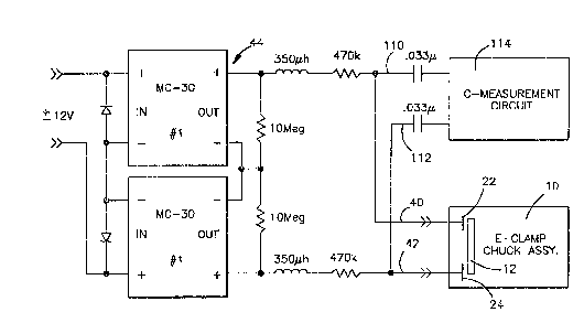
Figure 1 is a schematic of a power supply, electrostatic clamp assembly and
capacitance measuring circuit;
4
Figure 2 is a plan view of a wafer support used in an ion implanter;
Figure 3 is a view as seen from the plane 3-3 in Figure 2;
Figures 4 and 4A are schematics of a capacitance sensing circuit;
Figure 5 is a power supply circuit for energizing the sensing circuit of
Figures 4 and 4A;
Figure 6 is a schematic of a control system that utilizes an output of the
capacitance sensing circuit of Figures 4 and 4A to control an ion implanter;
and
Figures 7 and 8 are schematics of circ:uitry for controlling a polarity of an
output from the power supply Shawn in Figure 1
Best lVlode For Practicin~the Invention
The drawings illustrate a clamp assembly 10 for supporting and holding a
semiconductor wafer 12 (Fig. 3) for processing. The clamp assembly 10 includes
a
backing plate 14 which is preferably formed of alumina or molybdenum, a base
member 16 also formed of alumina, a dielectric layer 18 of glass, and a
dielectric
layer 20 of alumina. Electrodes 22, 24 are interposed between the glass layer
18
and the dielectric layer 20 and a heating element 26 is interposed between the
glass layer and the base member 16.
A gas fitting 28 extends through the chuck assembly opening into the
.20 interface between the wafer and the layer 20 to provide gas conduction
cooling
between the wafer and the chuck as described in U.S. Patent I~o. 4,261,762. A
gas
distribution graove 29 is formed in the top surface of layer 20 to aid in the
distribution of the gas.
The base member 16 defines a manifold having a channel 30 for the flow of
a cooling fluid. In the preferred embodiment shown, the channel is formed as a
spiral; however, it can also follow a meandering path or it can be a series of
interconnected channels. The channels are closed to define an enclosed conduit
or conduits by means of the backing plate 14, which is sealed against the
manifold.
Openings are provided in the backing plate for a coolant inlet fitting 32 and
a
coolant outlet fitting 34. Since the present chuck assembly is intended to
perform
under a wide range of temperature conditions, the cooling medium flowing
through the manifold can be either a liquid or a gas, depending on the
application.
5
Clamp Construction
The dielectric layer 20 is preferably formed of a thin (about .25 mm) layer
of high purity (99.5%) alumina. The electrodes 22, and 24 are then formed on
the
bottom (as seen in Fig. 2) surface of the dielectric layer, preferably by
screen
printing a paste of powdered copper aluminum or silver palladium metals and
glass frit onto the dielectric layer and then (ring it at about 700°C.
As shown in
Figure l, the electrodes are essentially half circular in plan view.
The heating element 26 is formed by screen printing a paste of powdered
tungsten and glass frit onto the manifold in the form of a continuous meander,
the
geometry of the meander preferably being as shown in Figure 3 to provide a
higher heater power density at the outer edge to optimize temperature
uniforznity
across the chuck.
Once the electrodes 22, 24 and heating element 26 are fired onto the
dielectric layer, the layer 20 is bonded to the manifold. After the above
assembly
I~ is complete, the backing plate 14 is furnace brazed or sealed by means of a
sealing
glass to the bottom of the manifold 16.
As shown schematically in Figure 3, access holes 36, 38 are formed through
the backing plate 14, the manifold I6 and the dielectric layer 18 for a first
conduc-
tor 40 connected to the electrode 22 and for a second conductor 42 connected
to
the electrode 24. The conductors 40, 42 are attached to the electrades by
brazing
or other convenient methods such as by providing spring contacts engageable
with
the electrodes and are connected to a power supply 44 (Fig. 1) which provides
a
signal of about 3 kilovolts DC to create the electrostatic clamping force to a
semiconductor wafer 12 placed on the surface of the dielectric layer 20. The
power supply 44 includes two modules 44a, 44b which are coupled together to
provide a bi-polar output.
Access holes 46, 48 are also formed through the backing plate 14 and the
manifold 16 for a third conductor 50 attached to one terminal of heating
element
26 also by brazing or the like, and fourth conductor 52 similarly attached to
the
other terminal of heating element 26 to connect the heating element to a
second
power source 54, typically operating at I20 volts. Preferably, the access
holes 36,
38 and the hole for the gas fitting 28 are machined into the structure with
the
~1:L~~~~l~
6
holes 3S, 38 sealed with sealing glass and the fitting borvded into its hole
with
sealing glass.
Capacitance Sensin~Circuit
.As seen in Figure 1, two inputs 110, 112 from the electrodes 22, 24 are
coupled to a capacitive sense circuit 1I4. A capacitance across these two
inputs
110, 112 corresponds to the capacitance between the electrodes 22, 24 and is
influenced by the presence of a wafer as well as the voltage applied to the
electrodes. These two inputs are coupled to an operational ampliber 120 within
an integrated circuit 122. The integrated circuit is a commercially available
circuit
designated LF 356 and can be obtained from hlational Semiconductor.
The operational amplifier 120 generates an output which oscillates with a
frequency directly related to the capacitance between the inputs 110, 112.
The oscillating output signal from the operational amplifier 120 varies
between 0 and 5 volts. This signal is shaped and then coupled to a comparator
amplifier 130 having a reference input 132 defined by a zener diode 134 at _
approximately 5 volts. The comparator amplifier 130 creates a square wave
signal
output having a 500lo duty cycle having an ~l~ period that varies depending on
the
sensed capacitance. For a 4-inch circular diameter wafer, this period is
approx-
imately 20 microseconds with no wafer in place, 30 microseconds with a wafer
placed on the layer 20, and 40 microseconds with the wafer in place and a
clamping voltage (approximately 3 kilovolts) applied to the electrodes by the
power supply 44.
An output from the comparator amplifier 130 toms on and off light-
emitting diodes I40, 142 which are optoisolated from corresponding photodetec-
tons. A top photodetector 144 is used for diagnostic purposes and an output
I48
from the detector 144 can be coupled to an oscilloscope, for example, for
monitor-
ing frequency changes with capacitance.
A second photodetector 146 generates a signal which turns on and off a
transistor 150 which i s coupled to an analog switch 152 (Fig. 4.~). This
analog
switch 152 has in input (I1~T) coupled to the collector of the transistor 150.
As the
transistor turns on and off, outputs (SI, 52) of the switch 152 sequentially
change
state from ground to 8 volts in accordance with the square wave frequency
output
from the comparator 130.
The output from the analog switch 152 is integrated by a resistor, capacitor
circuit 154 so that the input to a non-inverting input 160 of an operational
am-
plifier 162 is a voltage level directly related to the capacitance sensed by
the circuit
114. This operational amplifier 1.62 operates as a voltage follower so that an
output 164 designated FVC~UT is a I3C output signal directly related to sensed
capacitance. This L7C output signal is used 'by an implanter control system
250
(Fig. 6) to monitor performance of the system. The wafer handler for
depositing a
wafer onto the chuck is activated in response to an appropriate no wafer
condition
being sensed. ~nce the wafer is sensed, an output from the control circuit 250
activates the I3C power supply 44 to energize the electrodes 22, 24 causing an
electrostatic attraction between the clamp and the wafer.
Turning to Figure 5, this figure discloses a power supply circuit 200 for
generating voltages appropriate for the capacitance monitoring circuit 114.
Two
inputs 210, 212 at the left of Figure 5 provide a voltage which energizes a
light-
~emitting diode 213. This voltage produces a 12-volt signal due to the voltage
clamping operation of a zener diode 214. The 12-volt signal is then coupled to
integrated circuit voltage regulators 216, 21g for producing +g and +5 volts.
A
DC to DC converter 220 provides plus and minus 15-volt signals. These voltages
are applied to the circuitry of Figures 4, 4A for providing the capacitance
mon-
itoring capability of the present invention.
Wafer Release
The implanter control system 250 of Figure 6 interfaces with a wafer
release circuit 300 depicted in Figures 7 and g that activates the power
supply 44
with the bi-polar output configuration. The circuit 300 includes a logic
driver
circuit 310 having two outputs OUTl, OUT2 coupled to two power supply
modules 44a, 44b. The power supply modules are preferably 1°dIC-30
power
supplies commercially available from Oamma High Voltage of ~rmand Beach,
Florida. Two inputs IN1, IPd2 control the outputs ~UTl, ~~.TT2. When Hell is
positive, the output t~~tJTl from the logic circuit 310 is positive and acts
as a
current source so a first power supply module 44a is activated. When this h; p-
pens, the voltage across the two electrodes mounted to the wafer support is of
a
first polarity. ~Ihen IN2 is positive, the output designated ~UT2 from the
logic
circuit 310 is positive and acts as a current source and the second switching
power
supply module 44b is active so the polarity of the voltage across the
electrodes is
switched. The circuit 310 is commercially available from i~S Thompson under
part designation L,6202.
after a wafer is placed on the support layer 20, prior to wafer implantation,
one module of the power supply 44 is activated to maintain an electrostatic
attraction between wafer and support. To accomplish this, an EI~1~I~E input
312
to the circuit 310 is high and one or the other of the inputs IN1, IN2 remains
positive during ion implantation. 'This causes a fixed voltage to be applied
to the
electrodes 22, 24 maintaining electrostatic attraction between the wafer and
the
support.
Wlxen the wafer is to be released from the support, the enable input
EIoIABLE to the circuit 310 remains high, but the two inputs I1~T1, IlV2 are
alter-
nately turned on and off by means of the Q and not Q outputs from a flip-flop
320. The frequency at which the polarity of the power supply is switched is
controlled by an input 322 to the flip-clop 320. The flip-flop is configured
as a
divide-by-two counter so that if the signal at the input has a frequency f,
the
outputs change state at a frequency of f/2. Then the Q and not Q outputs
switch,
a different one of the modules 44a, 44b is activated, effecting a switching of
polarity across the electrodes within the wafer support.
Turning~now to Figure 7, the input 322 to the flip-flop 320 originates from
an ~ gate 330 having two inputs 332, 334. one input 332 to the gate
330 depends upon control signal from the controller 250 which is applied
across
two inputs 34U, 342 to an optoisolator 344. then an input 340 is positive with
respect to the input 342, current flows through a light-emitting diode 344a
within
the optoisolator, activating a photosensor 344b. This generates a low output
which
is coupled to the input 332. The voltage across the two inputs 340, 342 is
applied
by the controller 250 when the controller has sensed the presence of a wafer
on
the support and responds to this sensed condition by activating the
electrostatic
attraction between the wafer and t'xe support.
~ ~~.~~3~:~9
When a clamp activation voltage is applied by the controller 250 to the
inputs 340, 342, the signal on the input 332 to the AND gate 330 goes low
causing
the output from the AND gate 330 to go low and maintain the flip-flop 320 in
one
state (which state is not important during clamping). As seen in Figure 7,
this low
output signal from the optoisolator 344 is also applied to a negative ~R gate
350
having an output coupled thraugh an invertor 352 to an AND gate 354 (p'igure
8).
A low output from the optoisolator 344 caus~;s the AND gate 354 output to go
high, causing the enable input 312 of the logic driver circuit 310 to receive
an
activation signal. The state of the two inputs IN1, IIV2 causes one or the
other of
the modules 44a, 44b to be activated so that a voltage difference is applied
to the
electrodes within the wafer support. This activates electrostatic attraction
between
the wafer support and wafer. A second input to the AND gate 354 from an
invertor 353 receives a hardware generated wafer sense signal derived from the
FVO~CTT signal 164.
Subsequent to ion implantation, the controller 250 de-activates the electros-
tatic attraction by providing a control signal to cause the polarity of the
voltage
applied to the wafer electrodes to change back and forth, thereby dissipating
the
electrostatic energy between wafer and electrode.
When the controller 250 de-activates wafer clamping, the output signal from -
the optoisolator 344 goes high, therefore, assuring one input 332 to the AND
gate
330 is also high. 'Two additional controller generated inputs 360, 362 are
coupled
to a second optoisolator 364. When the voltage at the input 360 is more
positive
than the voltage at the input 362, this second optoisolator 364 is activated
and a
low output from the optoisolator is coupled through an invertor 366 and, there-
fore, goes high. This high-input signal is coupled to a first one-shot 370,
causing a
Q output 372 from the one-shot 370 to go high. The not C~ output
simultaneously
goes low and is coupled to the gate 350 for enabling the drive circuit 310.
Thus,
even though the signal 340 from the controller is removed, the drive circuit
is still
enabled. The t~ output from the one-shot 370 is coupled to a second one-shot
380
which is configured as an oscillator circuit. The Q output from this one-shot
is fed
back to the activation input through an external circuit which causes the
second
one-shot 380 to oscillate with a predetermined frequency of approximately 20
hiz.
10
This causes the input 334 to the AND gate 330 to be pulsed at this frequency.
As
noted above, the O-Utpllt of the AND gate 330 is coupled to the flip-flop
which acts
as a divide-by-two counter. This causes the polarity on the electrodes to
oscillate
back and forth for a time period equal to the; output time of the first one-
shot 370.
After the one-shot 370 times out, the Q output from this one-shot de-activates
the
oscillator one-shot 380 and also removes the enable signal from the circuit
310.
In accordance with a second embodiment of the controlled release mechan-
ism of the invention, the controller 250 directly activates the inputs 340,
342 for
controlled ON/C)FF intervals. The junction 322 is low when the input 340 is
high.
:E3y clocking the input 340 at a controlled or adjustable rate, the frequency
of
switching from the circuit 310 is controlled which, in turn, controls the
polarity
switching of the two power supply modules 44a, 44b. Three jumper connections
P1, P2, P3 at the input to the one-shot 370 are set depending on whether the
controller performs the switching or the combination of one-shot 370 and mul-
tivibrator 380 control the switching. A jumper across P1 and P2 disables the
one-
shat 370, and a jumper across P2, P3 enables the one-shot.
~~eration
In operation, a wafer 12, which is to be processed, is placed upon the
surface of the layer 20, and the supply 44 will be energized to apply an
electros-
tatic attractive force between the wafer and the layer 20 sufficient to
maintain the
wafer in position on the chuck. The chuck 10 can then be both rotated and
translated to bring the wafer to a wafer treatment station such as an ion
implan-
tation chamber.
The implanter control system 250 (Fig. 6) has a large number of device
interfaces which receive inputs from sensors 252 (for example, gauges
measuring
pressures, voltmeters, encoders measuring mechanical position, and the
F'~l~I;JT
output 164), and send operating commands to mechanical and electrical com-
ponents 254 (for exaanple, valves, power supplies, robots, and the
electrostatic
clamp power supply 44).
Within the control system there are programmed a variety of cross checks
which must be performed before sending an operating command (for example, the
valve to a cryopump ~canroi be opened unless it is verified that the chamber
is
=~:~~~~~:~~J
11
already under rough vacuum). The output 164 indicates the wafer's presence and
whether it is clamped and provides critical information for these cross checks
to
implement wafer handling and implantation operations. For example, the as-
sembly 10 would not be rotated into a vertical position unless the wafer was
verified to be securely clamped. Similarly, the clamp would not be activated
unless the wafer's presence on the clamp was verified. 'EJVhen a critical
cross check
fails, the control system 250 has the ability tca place the implanter into 1-
IOLl~
(suspend further operation) in order to avoid damage to the machine or to
produce wafers.
A second function of the series of cross checks is to provide an operator
interface 260 information about machine status. Specifically, when a cross
check
fails, an alarm message is generated for display on an operator interface
screen,
and is recorded in a data log maintained on a disk drive. This information
permits
an operator to take corrective action to restore norrnal machine operation.
Once the wafer has been ion treated, the assembly I0 is moved to position
the wafer for removal from the support. The controller 250 then either signals
the
one-shot 370 to activate polarity reversal of the power supply 40 or directly
switches that polarity at a controlled frequency. The electrodes are biased
with
alternating polarity and release the wafer by reducing electrostatic
attraction
between the wafer support and the wafer.
Figure 6 represents current state-of the-art for control equipment. The
addition of the capacitive sensing circuit 114 and the wafer release circuit
300
represents an advance in the quality of information available about the status
of
the wafer on the clamp 10 and the ability to efficiently treat wafers.
5~hile the preferred embodiment of the invention has been described with a
degree of particularity, it is the intent that the invention include all
modifications
and alterations from the disclosed design falling within the spirit or scope
of the
appended claims.