Note : Les descriptions sont présentées dans la langue officielle dans laquelle elles ont été soumises.
2~6~
Backgroolld of the Invention
The present invention relates to high frequency power supplies forneon and
other gaseous luminous tubes and, more specifically, to apparatus for the sensing of
certain anomalous load or load fault conditions and ~or the subsequent interruption of
the supply output in response thereto.
Ground fault detection is a well known subset of load fault detec
tion/interruption inwhich an unbalanced load is detected by monitoring forany 'differ-
ential', i.e. unequal, currents between the respective high voltage output leads. Such
unbalances are, by definition, the result of a shunting of current through a ground
return path. Under ordinary circumstances these ground faultcurrents are caused by
human contact with, for example, an exposed connection of a luminous neon sign.
Upon detection of such a 'fault' condition, the power supply is generally disabled until
cessation of the fault cond;tion. In this manner the principal objective of this form of
load fault detection and interruption - - the protection of persons and pets against
electrical shock - - is achieved.
It is deemed prudent, however, to provide power supply intelTuption in
response to other anomalous opeMting conditions, for example, following the failure
of one or more luminous tube sign segments, due to breakage or otherwise. Com/en-
tion ground fault interruption circuits have not always proved satis~actory under the
diversity of load fault conditions associated with neon tube failure or breakage.
In multiple tube luminous sign topologies, where forexample two or more
neon tube segments are placed in an electrical 'series' configuration, the breakage of
one tube often precipitates a current imbalance not too dissirnilar to that caused by
inadvertent human contact. Due to the inherent distributed capacitance of neon tube
segments, the breakage of one segment does not necessarily cause the total and
complete interruption of current through the entire series loop. Indeed, depending on
the location ofthe breakage (i.e. the locations ofthe remaining good tube segments),
21 ~86~
a distributed capacitance in the order of 10-40 picofards willfacilitate a corresponding
10-30 milliampere current flowthrough one (or both) of the power supply high voltage
leads with such distributed capacitance forming a 'ground' return connection for these
currents.
In most eases, the breakage of a single tube segment results in the total
cessation of current in one high voltage lead or, at least, a significant imbalance be-
tween such leads. Under such circumstances, the current imbalance triggers the
conventional ground fault interruption circuitry in the normal fashion thereby shutting-
down power supply operation as required.
But this result is not assured. For example, in a multiple tube arrangement
where the center tube only is damaged, the current in both of the high voltage power
supply leads may be substantially equal thereby defeating normal ground fault interrup-
tion operation. Sustained operation under such fault conditions may, in turn, cause
failureofhigh voltage power supply. More specifically, resonance between the distrib-
uted capacitance of the remaining 'good' tube segments and the high voltage trans-
former secondary can produce unexpectedly high output voltages which, inturn, may
eventually destroy the transformer through turn-to-turn shorts or insulation breakdown.
Tlhe present invention therefore relates ~o a load fault interruption arrange-
ment particularly adapted to disable high voltage/high frequency luminous tube power
supplies under reduced, but balanced, load faultconditions. Itwillbe appreciated that
the present load fault system may be employed advantageously in combination withconventional ground fault interruption circuitry whereby the actual power supply 'inter-
ruption' or shut-down apparatus of the latter device may be additionally utilized in
similar fashion by the present load fault detection systern thereby obviating the ex-
pense associated witlh the replication thereof.
In addition to the above-noted output voltage increase (e.g. from 3KVto 6-
12KVpeak), ithas been discovered that the output waveform ofthe 'i~aulted' neon sign
21~8~2~
contains significantly higher harmonic content as compared to the normally operated
high frequency neon sign. Anormally operated high frequency luminous tube power
supply may contain as littleas 5-10% harmonic distortion while the ha~monic output Gf
a faulted supply may be as high as 30-60%.
The present invention advantageously utilizes both attributes - - i.e. in-
creased harn~onic content as wellas increased overall output voltage - - to achieve a
positive indication of a faulted, or broken, luminous tube condition. More particularly,
a single-pole RC high pass filteris coupled to a high voltage secondary lead with the
output therefrom, in turn, connected to a detector/comparator. As itis necessary to
lower the detected voltage from the normal luminous tube operating voltage (e.g. 3-9
KV)to a much lower trigger level (e.g. 0.5-10 volts), the high pass filter'doubles' as
an attenuator by appropriately selecting the filtercut-off or corner-frequency. Typical
filtercorner-frequencies in the order of 150 MHz have been found satisfactory.
A significant advantage of the above-described combination filter/attenuator
is the corresponding reduction incomponent values required therefor. The series high
pass ~lltercapacitance, for example, need be only in the order of about 3 picofarads.
In a preferred embodiment of the present invention this capacitance is ine~pensively
secwred simply by adhering a small section of metali~ed tape or foil(e.g. 3/8"x3/4")
to the side of the high voltage transformer.
To avoid false fault triggering otherwise observ~i to occur upon initialsign
energization, the present load faultdetector incorporates a detection delay of approxi-
mately one millisecond . Research has revealed that non-ionized neon tube segments
appear, electrically, as open or 'faulted' tubes until such tubes have fullyionized. This,
in turn, results in a transient turn-on condition resembling that of a broken tube.
Again, an extremely inexpensive and e~ficacious implementation (of the delay
circuit) is achieved by selecting a relatively large detector filtercapacitor as contrasted
2~8~2~
with the capacitor of the high pass filterthrough which the detector capacitor must be
charged.
The above-described load faultdetector performs wellwithvarious interrupt-
er technologies including SCR and triac-basecl circuitry. Indeed not extrinsie delay
capacitance may be re~quired with the triac apprs)ach as the inherent time delay of the
gate trigger input provides the requisite turn-on delay.
It is therefore an object of the present invention to provide load fault detec-
tion and interruption for a high frequency, high-voltage luminous tube power supply
that is inexpensive to construct; that detects and responds to certain load fault condi-
tions without regard to whether such faultis balanced, that is, without regard to wheth-
er there are in fact any ground fault currents associated therewith; that detects and
responds to over-voltage conditions occasioned by the loss of luminous tube seg-ment(s); and that may be used in conjunction with conventional ground fault interrup-
tion circuitry.
These and other objects aIe more fullyexplicated inthe drawings, specifica-
tion, and claims that follow.
Br~ef Descripeion of the Drawings
Figure 1 is a block representation of a high frequency luminous tube power
supply incorporating ground fault de~ection and the load faultdetection/interruption of
the present invention;
Figure 2 is a block representation of one embodiment of the load fault
detector of Figure l;
Figure 3 is a block representation of another embodiment of the load fault
detector of Figure l;
Figure 4a is a waveform diagram of the vol~age waveform output of the filter
of Figures 2 and 3 under normal power supply load conditions;
211862~
Figure 4b is a waveform diagram of the voltage waveform output of the filter
of Figures 2 and 3 under faulted power supply load conditions;
Figure 5 is a schematic diagram of one embodiment of the present invention
shown interfaced to a high frequency luminous power supply having an SCR-based
ground fault interrupter;
Figure 6isa schematic diagram of an alternative embodiment ofthe present
invention shown interfaced to a high frequency luminous power supply having a triac-
based ground fault interrupter;
Figure 7 is a perspeetive view of a high frequency, high voltage transformer
as shown in Figures 5 and 6 illustrating construction of the attenuator/filter capacitor;
and,
Figure 8 is a front elevation view of the transformer of Figure 7.
21~8~2!1
Description of the Preferred Elmbodiment
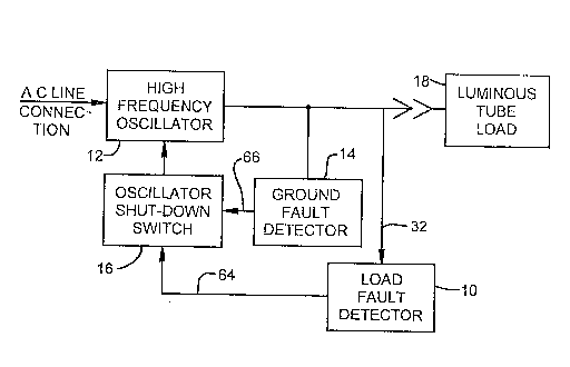
Figure 1 illustrates the present over-voltage and load faultdetector 10 incor-
porated into a generally conventional high frequency luminous tube power supply 12
including ground fault detection 14 and interruption 16 cirs~uitry also of generally con-
ventional design. The present fault detection/interruption apparatus is suitable for
inclusion into virtuallyany high ~requency power supply topology including free-running
power oscillators and fixed or free-running low power oscillator/power switch combina-
tions.
Regardless ofthe specific topology utilized, substantially every high frequen-
cy luminous tube power supply employs an output step-up transformer having a high
voltage secondary winding (typically 3-9KV) which in turn is connected to the gaseous
luminous tube load 18 (Figure 1). The ground fault 14 and load fault detec-
tion/inte~uption 10 are additionally interconnected to this secondary winding as shown
in more detail in Figure 5.
Referring to Figure 5, transformer 20 defines the output portion of high
frequency power supply 12 (Figure 1) and includes a center-tapped high voltage
secondary winding 22 connected to a luminous tube load comprised, as illustrated in
Figure 5, of three series-connected luminous tube segments 24. The secon~l.ary
center-tape 26 operatively connects to the ground faultdetector 14 (Figure 1), the latter
detector functioning in conventional manner to monitor and detect the presence of
currents flowing through such center-tap connection.
Under normal operating conditions no current flows in this conductor. The
presence of a center-tap current, there~ore, indicates a 'ground fault'condition which,
upon reaching a predetermined threshold level, triggers switch 116 (Figure 1) to termi-
nate further oscillator/power supply operation. It will be appreciated that various
devices may be selec~ed for switch 16 including, for example, the SCR ~8 of Pigure 5
or the triac 30 of Figure 6, bipolars, FETs and opto-isolators.
2~862~
Ground fault intermpters are well known in the art and willnot be discussed
in detail herein except to emphasize an important economy-producing feature of the
present invention wherein a single interrupter switch 16 may be employed to achieve
power supply shut-down upon detection of either a conventional ground fault or an
over-voltage or defective/broken tube segment fault.
One embodiment of the over-voltage/load fault detector 10 of the present
invention is shown in block form in Figure 2. Detector 10 input 32 is preferably con-
nected to one of the high voltage secondary leads of transformer 20 (see Figure 5)
where itis fi~rstfiltered by high pass filter34. As detailed further below, Figures 4a and
4b illustrate the output waveforms at 36 from filter34, respectively, under normal and
faulted load conditions. These filtered waveforms are thereafter connected to
comparator/detector 38, the function of which is to generate a shut-down gating signal
at 40 when a predetermined threshold voltage from filter34 is exceeded. This gating
signal is passed, in turn, through a delay network 42, then, to the previollsly discussed
shut down switch 16.
Tofullyappreciate operation of load faultdetector 10,ref~rence ismade to
the voltage waveforms of Figures 4a and 4b. More specifically, a comparison of
normal and faulted power supply output waveforms reveals an important distinction,
namely, that the harmonic content nf the output dramatically increases under most
faulted load conditions. Thus, differences between the normal and faulted power
supply output waveforms, which might otherwise appear less than significant, may be
significantly magnified by processing the supply output, for example, by applying the
power supply output to an appropriate filter. Figures 4a and 4b represent just such
processed waveforms, more specifically, the power supply output voltages at 36 after
passage through filter34.
Filter34 is of the single-pole high pass variety having a cut-off or corner fre-quency well above the power supply operating frequency. Itwillbe appreciated that
2~.1862~
other filtertopologies may be employed, however, the straightforward single-pole high
pass arrangement shown herein is both sufflcient and economically suitable. Filter34
may additionally and advantageously double as an attenuator. l'ypically 60-80db of
attenuation is required to lower the power supply output voltage from its nominal 3-9KV
.~.
level to the O.S-lO volt logic-level required of most sigr~l processing circuitry, in particu-
lar, the comparator/de~ector 38 to which the filteroutput is subsequently connected.
lFigure 4a represents filter34 output waveform when connected to a typical
high frequency power supply operating under normal load conditions. ~igure 4b is the
same waveform when the supply is subjected to a faulted load such as a broken ormissing luminous tube segment. Itwillbe observed that the waveform of Figure 4b
contains more harmonic content and is of a higher absolute magnitude. This latter
condition is due, in part, to the former - - filter34 attenuates the harmonic frequencies
less and consequently passes more total energy under the harmonic-rich faulted load
condition of Figure 4b. The filtered waveform of Figure 4b may also be of greater
magnitude due to an absolute increase in the power supply output voltage under no
or reduced load conditions.
The above-discussed output-to-detector attenuation may be achieved with-
out resort to further components or complexity by selecting a suf~lciently high filtercut-
off frequency - - the higher the cut-off frequency, the greater the attenuation. As
discussed below in connection with Figure 5, a cut-off frequency in the order of150MHz has been found appropriate.
Referring again to Figure 2, the filtered power supply output is connected
to comparator/detector 38, the function of which is to output, at 40, a signal whenever
the input signal level to detector 38 exceeds a predetermined level. This level is depict-
ed as Vrr~ in Figures 4a and 4b and is selected such that the output from filter34 does
not exceed YrO,during normal operation but does exceed V~f under broken, missing,
or other similar faulted load conditions. Again, Figures 4a and 4b illustrate, respective-
Iy, the normal and faulted load conditions with the filtered signal lev~ exceeding the
threshold, V,0~, only in the latter faulted-load case.
A delay circuit is interposed between detector 38 and the oscillator shut-
down switch 16 (Figure 1) to force an approximately 1 millisecond delay in the deacti-
vation of the high frequency power sllpply 12 . It was found that in the absence of this
delay function, false power supply shut-downs could occur upon initialpower supply
activation. Investigation revealed that a perfectly 'healthy' gaseous luminous tube
nevertheless appears electrically very similar to a broken tube until the gas medium
therein has become sufficiently active, i.e. ionized.
Itwillbe appreciated that several permutations are available and contemplat-
ed by the present invention with respect to the detector/comparator/delay functions.
There is not, in short, a prescribed implementation or order to these functions and
consequently other embodiments willperform satisfactory so long as the basic required
functions are replicated thereby. Figure 3 is an e~ample in block form of one such
alternative arrangement. Figure 5 is a schematic implementation of the embodiment
~0 of Pigure 3.
Referring therefore to Pigures 3 and S, one terminal of the high voltage
power supply output is connected at 32 to high pass filter34, which filteris comprised
of series capacitor 44 and shunt resistor 46. The output therefrom, again designat-
ed 36, connects to detector 48 defined by the single component, diode 50. The recti-
fied output frorn detector 50 feeds shunt capacitor 52 which serves both as a conven-
tional filtercapacitor for the detector rectifier diode 50, but importantly as the delay
element 54.
Delay, in the present embodiment, is achieved by an appropriate selection
of the capacitances of, or more accurately the capacitance ratio between, capac-itors 441 and 52. As noted abov~, filter34 may advantageously double as an attenu-
atorbyselecting anappropriately highfiltercut-offfrequency, forexample, greater than
;
211~62~
1000 times the power supply operating frequency. Acut-off frequency of 160 MHz,as
employed herein, nets nearly 80db of attenuation at a fundamental power supply
frequency of 20 KHz. Typical values for high pass filtercapacitor 44 is 3 picofarads
and for resistor 46 is 330Q
Several additional advantages of economy flow from the extremely low
10 capacitance 44 permitted by this high-attenuation filterdesign. The firstrelates to the
delay function currently under consideration. More specifically, the effective source
impedance of the low 3pf filtercapacitance 44 precludes the instantaneous charging
of any substantial capacitive load. Thus, delay capacitor 52 is deliberately chosen to
effect the desired 1 ms delay by requiring approximately twenty power supply output
15 charging cycles in order to 'pump Up7 the voltage across capacitor 52 to the 0.5-10 volt
level required to trigger oscillator shut-down switch 16 (Figure 1). Capacitor 52 is
nominally 0.047~uf in the embodimcnt of Figure 5.
Referring still to Figures 3 and 5, the output from delay circuit 54 (delay
capacitor 52) is operatively interconnected to comparator ~6, in turn, to shut-down
20 switch 16 (Figure 13. Comparator 56 is shown in do~ted format to signify that the
comparator function may be ~ound in, and defined by, for example, the intrinsic gate
trigger potential of the solid-state switching device employed. Under such circumstanc-
es, no additional or specific comparator hardwars is required.
One such solid-state switch 16 is the SCR 28 of Figure 5 with its t~igger gate
25 input 58. Ihe typical gate ~rigger potential for an SCR is 0.6 Yolts. This potential
e~fectively serves as the comparator threshold or reference voltage, V,~ When the
output across delay capacitor 52, as scaled by voltage divider resistors 60 and 62,
exceeds 0.6 volts, this 'pseudo-comparator' function of the SC R gate 5$ is activated,
causing SCR triggering and power supply shut-down.
It will be observed in the ennbodiment of Figure 5, that the gate 58 of
SCR 28 is connected to both the output of the above-described load fault detector at
2~624
64 as well as to the Olltput of a conventional ground fault detector l4 (Figure l) via 66 .
In this manner, additional overall power supply economy is achieved by obviating the
need for multiple interrupter, shut-down switches.
As discussed above, use of a small high pass filtercapacitor 441 (e.g. 3pf)
isaccompanied by several economic-based design advantages including the previously
discussed essentially componentless incorporation ofthe delay timeras ancillary to the
otherwise required high pass/detector filtercapacitors 44 and 52. Asecond significant
benefit arising from this low-capacitance filterdesign is the ability to obtain and fabri-
cate this capacitor - - which capacitor must additionally be able to withstand the multi-
ple KVpower supply output voltages - - at virtuallyno expense by adhering a small
area of metali ation to the transformer exterior adjacent one of the high voltage sec-
ondary leads.
As shown in more detail in Figures 7 & 8, a region of metali~tion 70 is
placed on the outside of transformer 20 generally adjacent one of the high voltage
output leads 72. More specifically, the cylindrical region 74 shown represents the
ferrite transIormer core with primary and secondary windings thereon. Two of thetransformer leads, specifically the high voltage secondary leads 7~ are shown extend-
ing outwardly from the righthand portion of the trans~ormer. The generally cube-shaped solid 76 which surrounds the transformer windings, and onto the bottom ofwhich the meta1ization 70 is placed, is a dielectric potting matelial commonly employed
in high voltage transformer construction tv minimize vapor contamination and corona
problems. This po~ting material additionally serves as the dielectric for the capacitor
44 formed between metalization 70 and the high voltage lead 72 passing adjacent and
immediately thereover.
Figure 6 illustrates an alternative arrangement for the present load fault
detector connected to a triac 30 power supply shut-down switch 16 (Figure 1). Itwill
be observed that in similar fashion to the embodiment of Figure S, both conventional
1 1
;` 2~8~;2~
ground fault, at 66, and load fault, at 64, are provided and interconnected to a single
shut-down device, triac 78 in the apparatus of Figure 6.