Note : Les descriptions sont présentées dans la langue officielle dans laquelle elles ont été soumises.
CA9-93-022
METHOD AND APPARATUS FOR RETENTION OF A FRAGILE
CONDUCTIVE TRACE WITH A PROTECTIVE CLAMP
Fiel~ Of The Invent;on
The present invention relates to a method and apparatus for
retaining a conductive trace on a unitary clamp. More particularly
to an interconnect system designed to mount, secure, and protect a
conductive trace having a multi-lead integrated circuit. A clamp,
when assembled with a conductive trace having an integrated circuit
permits safe storage of the device, mounting of the device for
testing of the electronic components, and safe and accurate
mounting of the assembly on a printed circuit board during
production of the latter.
R~ckgrolln~ Art
The density of integrated circuits continues to increase and
as a result, the number of delicate leads between the integrated
circuit and a printed circuit board continues to increase. A
difficult problem still confronting engineers in the electronics
industry is an efficient and reliable way to secure an integrated
circuit to a board while maintaining electrical connection and
mechanical protection of the leads.
A fabrication process known in the electronics packaging art
is tape automated bonding (TA~3). A continuous tape of fragile
conductive traces, similar to, but far more fragile than
photographic film provides a basis for mounting integrated circuits
on each frame of the tape.
A metal pattern is formed on each frame of the conductive
trace. These metal patterns radiate from the center of the trace
CA9-93-022 2
where an integrated circuit is mounted to the peripheral edges of
the frame to form leads. The circuit is mounted such that the
contacts of the chip are mated with the corresponding metal pads in
the central portion of the frame. These fragile conductive traces
provide for electrical connection between the integrated circuit
and the circuit board.
The manufacture of electronic components, sub-assemblies and
assemblies requires a number of functionally different
manufacturing operations.
Manufacturing the fragile components is one operation. Testing
the component is another and final assembly is the last of these
different operations. The complex and additive nature of these
operations makes cost effective manufacture difficult. Each
operation requires unique and complicated equipment at the
manufacturing location. To perform these operations is not only
expensive, but there is also a relatively high possibility for
defective items.
United States Patent 5,099,392, entitled Tape-Automated
Bonding Frame Adapter System issued to the Hewlett--Packard company
on March 24, 1992, illustrates an adapter system for mounting an
integrated circuit and conductive trace to a circuit board.
The adapter system comprises three separate components to
mount the frame to a circuit board by building a sandwich of parts.
An adapter ring is positioned on a circuit board. A plurality of
conductive elements are wrapped around members of the adapter ring
to provide electrical connection between the circuit board and
conductive trace. The conductive trace is mounted over the adapter
ring. A seal is mounted over the conductive trace and finally a lid
is provided over the entire assembly to protect the conductive
CA9-93-022 3
trace. The entire assembly is secured in place by a number of
fasteners such as nuts and bolts.
United States Patent 4,696,526, entitled Carrier for Tape
Automated Bonded Semiconductor Device issued to the Intel
Corporation on September 29, 1987, illustrates a device for
mounting an integrated circuit and conductive trace to a base for
electrical test of the integrated circuit.
The device comprises two separate and complicated components
to mount a conductive trace by building a sandwich of parts. A base
is provided with a socket for receiving a conductive trace. The
conductive trace is positioned within the base by a plurality of
lugs. A cover is placed over the conductive trace and locked in
place with the base by a number of complementary locking members.
United State Patent 5,005,070, entitled Soldering Interconnect
Method and Apparatus For Semiconductor Packages issued to the
Hewlett-Packard company on April 2, 1991, illustrates a device for
attaching the outer leads of a semiconductor package to lands on a
circuit board.
The device comprises a frame structure that urges the edges of
a semiconductor package to the board. The frame structure is
secured in position either adhesively, or by thermal deformation of
stakes.
IBM technical Disclosure Bulletin entitled, Method of Bonding
Tape Automated Bonding Packages Using Conventional Surface Mount
Technologies, Vol. 34 No. 11 of April of 1992, illustrates a
temporary fixture that may be used in the assembly of a circuit
module with a printed circuit board.
A fixture temporarily grips the module in order to transport
and place the module on a printed circuit board. After a solder
CA9-93-022 4
process, the fixture releases the module and is removed for
recycling leaving the unprotected module behind. The circuit
module is relatively thick and durable compared to the circuit
trace contemplated herein.
The prior art references have a number of significant
deficiencies. Most systems have multiple components which are
costly to manufacture. Aligning a sandwich of components on a
circuit board is difficult, costly and time consuming. It is also
prone to error.
Retention of a fragile conductive trace having an integrated
circuit and retention on a circuit board in a unitary protective
structure is not disclosed. Conductive traces having integrated
circuits are stored and shipped separately from the mounting
devices. Separate storing of the unprotected conductive traces is
difficult due to the fragile nature of the traces and integrated
circuits. This typically requires additional protective packaging
for storage and shipping of components.
~mm~ry of The Tnv~nt; nn
It is a primary advantage of the invention to provide, a
unitary structure which permits retention of a very thin, fragile
conductive trace having an integrated circuit and retention on the
circuit board. In another advantage of the invention, the clamp
assembly is useful for safe storage, placement in a circuit test
apparatus, and mounting on a printed circuit board.
In a broad aspect of the invention, the invention consists of
a clamp having a base member for providing rigid support to a
conductive trace, a plurality of retention means extending
downwardly from said base member, each of said plurality of
~3
CA9-93-022 5
retention means having a retention section adapted for retaining
engagement with a plurality of corresponding apertures in said
conductive trace and each of said plurality of retention means
adapted for fastening engagement with a plurality of corresponding
apertures in a substrate.
In another broad aspect of the invention, the invention
consists of a conductive trace, a clamp, said clamp having a base
member, said base member having a plurality of retention means
extending downwardly from said base member, each of said plurality
of retention means having a retention section adapted for retaining
engagement with a plurality of corresponding apertures in said
conductive trace and each of said plurality of retention means
adapted for fastening engagement with a plurality of corresponding
apertures in a substrate wherein said trace is retained with said
clamp.
In another broad aspect of the invention, the invention
consists of a conductive trace, a substrate, a clamp, said clamp
having a base member, said base member having a plurality of
retention means extending downwardly from said base member, each of
said plurality of retention means having a retention section
adapted for retaining engagement with a plurality of corresponding
apertures in said conductive trace and each of said plurality of
retention means adapted for fastening engagement with a plurality
of corresponding apertures in a substrate wherein said trace is
retained with said clamp and said clamp is fastened to said
substrate.
The invention may include a standoff means to space a lower
surface of the base member a predetermined distance above a circuit
board.
7'
_,, ~ . .
CA9-93-022 6
The invention may also include a locator such as an
indentation trace formed in an upper surface of the base member to
permit centering of a material cutter for removal of the clamp.
In an embodiment of the invention, the base member is formed
by the upper surface, sidewall and lower surface of the clamp
structure. The substrate is a printed circuit board. The retention
means is a cylindrical post formed in plastic having a diameter
that press fits within an opening of the conductive trace. The
standoff means is a plurality of downwardly extending members
disposed at the peripheral edge of the base member or
alternatively, a rim formed in the posts.
It is another primary advantage of the invention to provide a
method to assemble a clamp with a fragile conductive trace having
an integrated circuit wherein the trace is retained in the clamp.
In another broad aspect of the invention, the invention
consists of a method of assembling a clamp with a conductive trace
having an integrated circuit comprising the steps of acquiring a
clamp from a clamp feeder and pressing the clamp onto a conductive
trace and retaining the conductive trace and integrated circuit
within the clamp.
In the drawings which illustrate embodiments of the invention.
Figure 1 is a axonometric view of a conductive trace retained
in a clamp mounted on a printed circuit board,
Figure 2 is a top view of the clamp,
Figure 3 is a side view of the clamp illustrating the posts
and the standoff,
Figure 4 is a bottom view of the clamp,
Figure 5 is another side view of the clamp illustrating the
posts and the standoffs,
7i.
CA9-93-022 7
Figure 6a is an expanded sectional view of the clamp taken
along line CC of Figure 2 illustrating the profile of a lower
surface of a clamp in an embodiment,
Figure 6b is an expanded sectional view of the clamp taken
5along line CC of Figure 2 illustrating another embodiment of the
profile of a lower surface of the clamp,
Figure 6c is an expanded sectional view of the clamp taken
along line AA of Figure 2 illustrating one embodiment of the posts,
Figure 6d is an expanded sectional view of the clamp taken
10along line AA of Figure 2 illustrating another embodiment of the
posts,
Figure 6e is an expanded sectional view of the clamp taken
along line AA of Figure 2 illustrating another embodiment of the
posts,
15Figure 7 is a top view of a tape with a plurality of
conductive traces,
Figure 8 is a single conductive trace excised from the tape,
Figure 9 is a top view of a conductive trace retained in the
clamp,
20Figure lOa is a bottom view of a conductive trace retained in
the clamp,
Figure lOb is an expanded sectional view of the clamp
illustrating an embodiment of the post cooperating with the trace,
Figure 11 is a top view of a printed circuit board
25illustrating the apertures which communicate with the posts of the
clamp to permit alignment of the clamp and the conductive trace
with the layout on the circuit board,
Figure 12 is a flow chart of the method to assemble a clamp
with a integrated circuit and a conductive trace,
CA9-93-022 8 ~~
Figure 13 is a schematic view of a di~ lan~ p~urality of
conductive traces having integrated circuits before exci'se of a
single trace,
Figure 14 is a schematic view of a die with a separated
single trace,
Figure 15 is a schematic view of acquiring a clamp from a
feeder by a vacuum nozzle for placement on a single trace,
Figure 16 is a schematic view of the clamp placed on a single
conductive trace for retaining the trace,
Figure 17 is a schematic view of removal of the completed
assembly of the clamp and conductive trace,
Figure 18 is a schematic view of the completed assembly
located in a test apparatus,
Figure 19 is a schematic view of the completed assembly
located in a shipping tube,
Figure 20a is a schematic view illustrating placement of the
completed assembly onto a printed circuit board, and Figure 20b is
a schematic view illustrating the completed assembly located on a
printed circuit board.
~e~;le~ nescr;pt;~n of ~he Preferre~ Embo~;m~nt
Referring to Figure 1, a clamp assembly is generally
illustrated at 10. An integrated circuit 14 located on a conductive
trace (not visible) is retained in the clamp 12. The clamp 12 is
mounted on a printed circuit board 16. The plurality of leads 18 of
the conductive trace communicate with the plurality of pads 20 on
the printed circuit board 16 for mechanical and electrical contact.
In final form, the leads are soldered to the pads.
Those skilled in the art will understand the clamp is formed
CA9-93-022 9
of plastic from an injection molding process. The plastic must be
suitable for withstanding high temperatures during a soldering
process and must have mechanical stability to protect the fragile
conductive trace and integrated circuit 14 from damage when
assembled as shown in Figure 1.
Referring now to Figure 2, features of the upper surface 30 of
the clamp 12 are shown. An aperture 24 is formed in the center of
the clamp 12. Location and size of the aperture 24 may be varied as
long as the aperture 24 permits visual inspection of information
located on a upper surface of the integrated circuit (not shown).
For example, the information may be a part number, or lot
number, or some other related technical markings.
During the assembly process or diagnostics after assembly, an
integrated circuit must be readily identifiable. The aperture 24
permits identification without having to add equivalent information
to the top surface of the clamp.
A plurality of recesses 22 are formed at the peripheral edges
of the clamp 12. These recesses 22 permit a visual inspection of
the leads 18 before assembly. After assembly, the recesses 22
permit a visual inspection of the solder joint between the leads 18
of the conductive trace 80 (see figure 8) and the pads 20 of the
printed circuit board 16 (refer to Figure 1.)
In the preferred embodiment, the clamp 12 is substantially
square having a recess 22 at the peripheral edge of each side to
permit inspection for each group of leads 18 (four groups not
shown).
A bevel 26 is formed on one side of the upper surface 30. The
bevel 26 permits orientation of the clamp assembly for correct
positional placement of the assembly on a printed circuit board 16
CA9-93-022 10
as the assembly must be electrically aligned with the board. The
bevel 26 also provides clamp orientation in a storage tube (not
shown). The bevel 26 also facilitates the use of vibratory feeders
during the assembly process.
A plurality of indentations 28 are formed in the upper surface
30 of the clamp. These indentations 28 are formed directly over the
downwardly extending posts 40 (see Figure 3). The diameter and
depth of an indentation is selected to loosely receive an end of a
post to permit tight stacking of the clamps 12. The indentations
also provide a visual indication from the upper surface 30 of the
clamp 12 to locate the posts 40 for removal of the clamp 12 from a
printed circuit board 16. A drill may be located over the
indentation to drill down through the upper surface 30 of the clamp
12 and effectively remove the post material or tape component
without damage to the printed circuit board 16. This permits easy
accurate removal of a clamp assembly, for example, upon electrical
failure of the integrated circuit 14, once assembled, for
non-destructive failure analysis.
Referring now to figures 3 and 5, side views of the clamp 12
are shown. The clamp 12 has a sidewall 46 formed of a suitable
thickness to provide mechanical rigidity of the structure and
protection of the fragile conductive trace and integrated circuit.
The clamp 12 is formed with an upper surface 30 and a lower
surface 44. A plurality of posts 40 extend downwardly from the
lower surface 44. The posts 40 engage apertures in the conductive
trace (not shown) for retention of the conductive trace within the
clamp 12. The posts 40 also engage apertures in the printed circuit
board 16 (not shown) to retain the clamp 12 on the printed circuit
board 16.
f~
CA9-93-022 11
The sidewall 46 has a plurality of standoffs 42 extending
downwardly at each corner of the clamp 12. The standoffs 42 are of
a length to control the height of the clamp 12 in a predetermined
spaced relationship with the printed circuit board 16.
The clamp assembly is effectively located on a printed circuit
board and pressed downwardly onto the board until the standoffs
engage the upper surface of the board providing the spaced
relationship. The function of the spaced relationship will be
discussed later with reference to Figure 20b.
Referring now to figure 4, a bottom view of the clamp 12 is
shown. From the lower surface 44, the downwardly extending posts 40
and standoffs 42 are shown. The cooperation between the posts 40
and the standoffs 42 permit retainment of the clamp assembly with
the printed circuit board 16 at a predetermined height above the
board.
While the preferred embodiment illustrates four posts and four
standoffs, those skilled in the art will appreciate the number and
placement of the posts 40 and standoffs 42 may vary without
departing from the scope and spirit of the invention.
Referring now to Figure 4 and Figures 6a and 6b which are a
cross sectional view taken along line CC of Figure 2, a profile of
the lower surface 44 is illustrated. The profile of the lower
surface 44 depresses the leads 18 of the conductive trace (not
shown) downwardly, effectively forcing the leads 18 of the
conductive trace down for engagement with pads 20 on a printed
circuit board 16 (refer to Figure 1.).
In one embodiment of the invention, a rectangular ridge 50 is
formed on the lower surface 44 of the clamp 12 as shown in Figure
6b. This ridge forms a rectangular shape around the lower surface
CA9-93-022 12
44 of the clamp 12 as shown in Figure 4. In another embodiment of
the invention, the lower surface 44 slopes downwardly and outwardly
from the center of the clamp 12 to depress the leads of the
conductive trace. The posts 40 retain a conductive trace 80 in a
plane beneath the lower surface of the clamp 12. This plane is
slightly above the lowest point of the lower surface or ridge in
order to create the downward force on the leads 18.
Sufficient downward force on the leads 18 will only occur if
the leads 18 lie below the plane of the integrated circuits 14
solderable surface as will be later described with reference to
Figure 2Ob.
Referring now to Figure 6c, 6d, and 6e, a sectional view taken
along line AA of Figure 2 illustrates the posts 40 extending
downwardly from the lower surface 44 of the clamp 12. As previously
described, the posts provide retainment of the conductive trace in
a spaced relationship with the clamp 12 and retainment of the clamp
12 with a printed circuit board 16.
In one embodiment, shown in Figure 6c, the posts 40 are
substantially cylindrical for engagement with apertures in the
conductive trace 80 (not shown) and apertures in the printed
circuit board 16 (not shown). A chamfer 60 located in a distant end
of the post 40 aids engagement of the respective apertures.
In another embodiment, shown in Figure 6d, the posts 40 are
substantially cylindrical, having a slot 62 extending from the
distant end of the post 40 inwardly to form two flexible post
members. The slot 62 permits inward flexation of these post members
to aid with engagement of the respective apertures and to provide
a tight press fit with the apertures of the printed circuit board
for retention of the clamp assembly 10.
- r
CA9-93-022 13
In another embodiment, shown in Figure 6e, integral standoffs
are formed in the posts 40. In this embodiment, the clamp 12 does
not require the standoffs 42 to provide the spaced relationship
between the clamp 12 and the printed circuit board 16. The post 40
forms an upper cylindrical surface 41 and a lower cylindrical
surface 45. The upper surface 41 communicates with the aperture 76
of the conductive trace 80 as previously described. The lower
surface 45 communicates with the apertures 90 of the printed
circuit board. The apertures 90 and lower surface 45 are of a
different diameter, being smaller than the upper surface 41. The
smaller diameter again must provide a tight press fit. A lip 43 is
formed at the junction of the upper and lower surfaces. The lip 43
provides the function of a standoff by resting on the upper surface
of the printed circuit board 16. The lip 43 is positioned on the
post to provide the predetermined spaced relationship between the
clamp 12 and the printed circuit board 16.
Referring now to Figure 7, a tape 70 of conductive traces 80
is shown. A plurality of sprocket holes 72 are provided at the
respective edges of the tape 70 to control movement of the tape
during the manufacturing process.
Electrical connection between the integrated circuit and a
printed circuit board is achieved by a single conductive trace 80.
A plurality of leads 18 is shown on each conductive trace 80. The
leads 18 are for electrical engagement with pads 20 on the printed
circuit board 16. A plurality of contacts 78 secure and
electrically engage an integrated circuit (not shown). A plurality
of lands 74 electrically connect the leads 18 with the contacts 78.
Formed in each conductive trace 80 are a plurality of
apertures 76. The apertures 76 engage the posts 40 (not shown) for
CA9-93-022 14
retention of the conductive trace 80 with the clamp 12.
In one embodiment, four circular apertures 76 are provided to
engage four cylindrical posts 40 on the clamp 12. The diameter of
the posts 40 and the diameter of the apertures 76 are such that a
press fit occurs between them providing retention of the fragile
trace without damage during the assembly process. The apertures
formed in the fragile film of the conductive trace 80 are
surrounded by metal patterns to strengthen the area for engagement
with the posts. The strengthened area resists tearing of the film
when engaged by the posts 40. It is appreciated by those skilled in
the art that minor changes to the number of, and shape of,
posts/apertures may be made without departing from the scope and
spirit of the invention.
Referring now to Figure 8, a single conductive trace 80 has
been excised and lead formed from the tape 70. The leads 18 are
formed in the shape of an S, as shown in Figure 14. The leads
could assume other shapes such as a gull wing.
Referring now to Figures 9, and lOa, a clamp assembly 10 is
shown. The conductive trace 80 is retained in the clamp 12 by the
engagement and cooperation between the plurality of apertures 76 in
the conductive trace 80 and the plurality of posts 40 of the clamp.
This assembly 10 may be stored in a shipping tube, or temporarily
placed in a test apparatus and then removed, or retained by a
printed circuit board. An integrated circuit is not shown in
Figures 9 and lOa.
Referring now to Figure lOb, a sectional view of a post is
shown cooperating with a conductive trace 80. The aperture formed
in the conductive trace 80 includes a plastic layer 81 having a
diameter slightly larger than the diameter of the post, and a
- ç~
CA9-93-022 15
copper layer 83 having a diameter slightly smaller that the
diameter of the post. A peripheral edge of the copper layer 83
deflects downward when a post is inserted into the aperture. The
edge provides a biting engagement with the post, retaining the
conductive trace 80 with the post.
Referring now to Figure 11, a printed circuit board 16 is
shown as configured to receive a clamp assembly 10. A plurality of
pads 20 are arranged to engage the leads 18 of a conductive trace
(not shown). The engagement is both mechanical, to secure contact
by application of solder, and electrical. The pads 20 are
electrically connected to other parts of the printed circuit board
16 by lands 92 etched on the board.
A plurality of apertures 90 are arranged in a predetermined
spaced relationship on the board 16 for receiving a plurality of
posts 40 of the clamp 12 (not shown). Those skilled in the art will
appreciate that the arrangement of pads 20 and apertures 90 may be
modified without departing from the scope and spirit of the
invention.
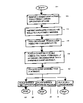
Referring now to Figure 12, the method to assemble a clamp
with a conductive trace will be described. The method starts at
110. A single conductive trace having an integrated circuit is
removed from a tape by application of a die to excise the trace.
The leads are formed by the complementary surfaces of the die
pressing the leads into an S shape (111), or other suitable shapes
such as a gull wing shape.
This single excised and lead formed trace is presented to a
placement machine (112). A clamp is then acquired from a clamp
feeder, for example by a vacuum nozzle (113).
The clamp is placed onto the single excised and lead formed
. ~
CA9-93-022 16
trace where the posts engage apertures. A downward force moves the
posts through the apertures a predetermined distance, without
damage to the conductive trace. This operation retains the
conductive trace with the clamp (114). The completed assembly is
acquired for placement at (115).
The completed assembly of a clamp and trace may be placed in
a storage package for shipping (117), or may be temporarily placed
in a test apparatus to electrically test the component (116), or
may be mounted on a printed circuit board (118).
Referring now to Figures 13 through 17, a schematic cross
section of the apparatus and components for the method to assemble
a clamp 12 and conductive trace 80 is shown.
In Figure 13, a tape of conductive traces 70 having integrated
circuits 14 is fed to an excise and lead form die, generally
indicated at 100. The die has an upper member 102 and a lower
member 104. The upper member 102 is operable to communicate with
the lower member 104 where a single conductive trace may be excised
from the tape 70 and the leads 18 may be formed during the same
operation. The leads are formed into a shape by the contour 106 of
the upper member 102 cooperating with the complementary contour 108
of the lower member 104 pressing the leads into shape. The result
is a single conductive trace 80 as shown in Figure 14.
A clamp is obtained from a clamp feeder 122 as shown in Figure
15 by a vacuum nozzle 120 and transported for engagement with a
conductive trace located in the lower member 104 of the die. The
vacuum nozzle 120 has a baffle over the aperture in the clamp to
permit suction to effectively grip the upper surface 30 of the
clamp 12.
As shown in Figure 16, the clamp 12 is aligned over the
-
CA9-93-022 17
conductive trace 80. This alignment operation centers the posts 40
directly over the apertures 76 of the conductive trace 80. The
lower member 104 of the die has a plurality of openings 124
directly under the apertures 76 of the conductive trace 80. The
size of the openings must be large enough to loosely receive the
posts 40 of the clamp 12 and small enough to support the
surrounding area of the conductive trace 70 as placed in the die.
A downward force drives the posts 40 through the apertures 76 a
predetermined distance to retain the conductive trace 70 in the
clamp 12. The posts 40 on the clamp 12 effectively press fit into
apertures 76 on the conductive trace 70 without tearing or damaging
the fragile conductive trace 70.
The lower member 104 of the die is contoured so that the
standoffs 42 of the clamp 12 do not touch or engage the die
surface. This permits the clamp 12 to be pressed downward to
unrestrictively receive the conductive trace 80 in a predetermined
spaced relationship without interference by the standoffs 42.
A completed assembly of a conductive trace 80 having an
integrated circuit retained in a clamp 12 is removed from the die
as shown in Figure 17. This assembly may be placed in a test cell,
a storage container, or provided for final assembly on a printed
circuit board.
Referring now to Figure 18, a completed assembly is shown in
a test apparatus 130. The test apparatus 130 is soldered directly
in place to a printed circuit board 16 in place of a completed
clamp assembly 10. The test apparatus 130 acts as an interposer
between the clamp 12 and the printed circuit board 16.
The test apparatus 130 is substantially a square box with an
operable lid 151. A plastic gate 132 pushes leads 18 onto its
CA9-93-022 18
contact pads 134 for electrical engagement. The upper surface of
the integrated circuit 14 is also pressed against a copper slug 136
by a protruding member 150 formed on the lower surface of lid 151.
A surface of the integrated circuit 14 communicates with a surface
of the slug 136 in order to dissipate heat generated by the
integrated circuit 14 under electrical test.
Thus the test apparatus provides both electrical and thermal
contact of the integrated circuit 14 for burn-in testing of the
integrated circuit 14 as retained within the clamp 12.
The lid 151 is pivotally connected at one end 152 to the side
of the test apparatus and releasably connected at another end 153.
These connections permit the lid 151 to operate from a closed
position for testing to an open position for insertion and removal
of a clamp assembly 10. The lid 151 is releasably locked in the
closed position in order to provide a downward force on the
integrated circuit 14 by the protruding member 150.
A plurality of copper posts 134 are soldered to pads on the
printed circuit board 16. The copper posts 134 extend upwardly
through the bottom 155 of the test apparatus 130 to form exposed
pads 154. The leads 18 of the conductive trace 80 contact the
exposed pads 154 for electrical connection during test of the
integrated circuit 14. The height of the copper posts 134 and slug
136 are such that the posts 40 of the clamp 12 do not engage the
apertures 90 of the printed circuit board 16 in order to permit
removal of the clamp 12 after the burn-in test. The bottom 155 has
a plurality of openings to loosely receive the posts 60.
The test apparatus 130 and gate 132 are designed so that the
leads 18 of the conductive trace 80 are not deformed. This allows
the clamp assembly 10 to be removed from the test apparatus 130
CA9-93-022 19
after burn-in for later use in the production of printed circuit
boards.
Referring to Figure 19, a completed clamp assembly 10 is shown
in a tube container 140 for storage and shipping. The overall shape
of the clamp 12 cooperates with the overall shape of the tube
container 140 to provide a single orientation of the clamp 12
within the container 140. The chamfer 26 of the clamp 12
communicates with a chamfer 142 of the container wherein these
chamfers must aline before inserting the clamp 12 into the tube
140. The inside dimensions of the tube are such that the clamp
assembly 10 may be slidably received and removed from the tube 140.
A single tube 140 may contain a plurality of clamp assemblies 10.
The clamp 12 protects the fragile conductive trace 80 from
damage that may occur from the top or sides of the clamp 12 by
combination of the upper surface, sidewalls, and standoffs of the
clamp. The four corners of the clamp extend beyond the ends of the
outer leads of the conductive trace 80 to protect the ends of the
leads 18 from handling damage.
In addition, the four posts 40 protect the outer leads 18 from
below. These posts 40 partially prevent damage of the trace 80 from
underneath by raising the trace above a smooth or level contacting
surface.
When the clamp assembly is placed in the tube 140, the trace
is completely protected from damage that may occur from
underneath the trace 80.
Tubes 140 containing these clamp assemblies 10 may be shipped
without damage to the printed circuit board assembly. The tube 140
may be used in a manufacturing process and provides the machinery
with the capability to determine the orientation of clamps for
-
-
CA9-93-022 20
placement on printed circuit boards.
Referring to Figures 20a and 20b, a completed clamp assembly
10 is shown on a printed circuit board 16. A placement machine
acquires an assembly from a feeder and locates the assembly over a
printed circuit board 16. The posts 40 of the clamp 12 are aligned
over apertures 90 in the printed circuit board. The machine pushes
the clamp 12 down onto the printed circuit board 16. The clamp 12
and conductive trace 80 are retained on the board by the posts 40
press fitting into the apertures 90 on the board. The clamp 12 is
eased down onto the board. The chamfers 60 on the posts 40 assist
with engagement between the posts 40 and apertures 90. The clamp 12
is then pushed down until the standoffs 42 engage the upper surface
of the board to engage the outer leads 18 of the trace 80 into
solder paste which has been previously screened onto the printed
circuit board 16.
The ridge 50, (see figure 4) depresses the leads 18 of the
conductive trace 80 downwardly, effectively forcing the leads 18 of
the conductive trace into engagement with the pads 20 of the
printed circuit board 16, prior to a soldering process.
The posts 40 engage the apertures 94 of the printed circuit
board 16 for retention of the clamp 12 on the printed circuit board
16. The length and diameter of the posts 40 and length and diameter
of the apertures 94 are such that a tight press fit occurs between
the sidewall of the post 40 and the sidewall of the aperture 94
preventing removal of the clamp 12 from the printed circuit board.
The posts 40 provide retention with the fragile conductive
trace 80 and retention with the apertures 90 of the printed circuit
board 16, once assembled to the printed circuit board 16.
The standoffs 42 rest on the upper surface of the printed
CA9-93-022 21
circuit board 16 to provide a predetermined spaced relationship
between the clamp 12 and the upper surface of the printed circuit
board 16. This spaced relationship must permit forced engagement of
the contacts 18 with the pads 20 and retain the printed circuit 14
at a distance above the printed circuit board 16.
Once a clamp assembly 10 is mounted on a printed circuit board
16, it provides mechanical protection to the delicate structure.
The printed circuit card assembly is then passed through a
surface mount technology reflow oven to form the various solder
joints. The clamp 12 remains in place on the printed circuit board
16 to provide mechanical protection to the fragile conductive trace
80 and integrated circuit 14. A surface of the integrated circuit
may be soldered to the printed circuit board 16 to provide for
cooling of the circuit. Optionally, an adhesive may be applied to
the back bond of the integrated circuit to provide for cooling.