Note : Les descriptions sont présentées dans la langue officielle dans laquelle elles ont été soumises.
~t21 ~38
APPARATUS AND METHOD EMPLOYING FAST POLARIZATION
MODULATION TO REDUCE EFFECTS OF POLARIZATION HOLE
BURNING AND/OR POLARIZATION DEPENDENT LOSS
T~- ' Field
S This invention relates to the optical ~ ;on of inl~ a~ion and,
more particularly, to improving l~ n;s~;on capabilities over long-distance optical
~""~.";c~;on paths employing re~ate.~.
Bacl~ u.-d of the I~ t;o.
Very long optical fiber trancrniscion paths, such as those employcd in
10 ul~df~ a or trans-co ~I;nf n~ terrestrial lightwave tr~nemic~ n systems in~l~Jdin~
optical-amplifier l~pcatc.~, are subject to dcc.~,asf,d performance caused by a host of
possible i,nl?a...llcnts. The in.~ ,,.f nt~ typically increase as a function of the length
of the optical ll .n-~n~ cn In long optical l.~n~...;c~ion paths that include optical
.l;f;f ~s, the i l-p~l,~nts tend to vary with time and cause a random fluctll~tion in
15 the signal-to-noise ratio (SNR) of the optical tr~ncmics;cn path. The random
~1l P - - - in SNR contributes to a ph~ .o.. - ~on known as signal fading. The SNR
flllrt~l~tione also result in an L.c.~;asf,d average bit error ratio (BER) in digital signals
being ~ l over the optical t i~ on path. When the SNR of a digital
signal being llans~ultcd on such an optical t~ on path becomes llQ~ce~l hly
20 small relative to the average SNR (resulting in an undei,~ably high BER), a signal-
to-noise fade is said to have occurrefl. E~p~ lf nldl evidence has shown that the
signal fading and SNR flnf tl~ if ~nS are caused by a number of pol~i7~tif n flepf n~1ent
effects induced by the optical fiber itself and/or other optical cfJ~ o~-f ~ within the
tral~crn;csion path. In particular, one of these effects has now been i~lf ntififA as
25 polC ;7~;1;f~ f3f'pef~fj1f~l~t hole burning (PDHB), which is related to the population
e~s;on dynamics of the optical amplifiers. A t1icc~lcs;on of hole-burning can befound in an article by D. W. Douglas, R. A. Haas, W.F. Krupke and M.J. Weber,
entitled "Spectral and pQl"''i7:-tiOIl Hole Burning in Neodymium Glass Lasers";
EEE Journal of Quantum Electronics, Vol. QE-l9, No. 11, November 1983.
PDHB reduces gain of the optical ~mrlifi~rs within the long optical
trancmiesion path for any signal having a state of pol~ri7~tion ("SOP") parallel to
that of a polarized primary optical signal carried by the l~ -a~ ;on path. II~,..v~e~,
the gain provided by these ~nlplifiP~ for optical signals which have an SOP
olll oe"n~l to that of the primary signal remains relatively ~ rf~ Ch ~ In ~
CA 02121738 1998-02-16
terms, the primary optical signal produces an anisotropic saturation of the
amplifier that is dependent upon the SOP of the primary optical signal. The
polarized primary signal reduces the level of population inversion anisotropically
within the amplifier, and results in a lower gain for optical signals in that SOP.
This effectively causes the amplifier to preferentially enhance noise having an
SOP orthogonal to that of the primary signal. This enhanced noise lowers the
SNR of the k~n.~mitte-l information and causes an increased BER.
A prior method for reducing signal fading employs a two-
wavelength light source to kansmit information in two orthogonal states of
10 polarization over an optical fiber tr~n~mi.s.~ion path. Since this light source shares
its optical power equally on any two orthogonal SOPs within the fiber, deleterious
polarization-dependent effects may be reduced as long as the two wavelengths
remain orthogonally polarized along the optical k:~n~mi.~.~ion path.
In accordance with one aspect of the invention there is provided
15 a~pa~dl~ls int~n~le~l for use in reclllcin~ the effects of polarization dependent hole
burning in an optical k~n~mi.~ion system employing optical fiber amplifiers
including means for generating a polarized optical signal at a desired wavelength
and means for supplying said polarized optical signal to said means for
mocl~ ting, the ~pa~dLus being CHARACTERIZED BY waveguide means having
20 an eleckooptically in~lnce-l variable birefringence for mo~lnl~tin~ the state of
polarization of said polarized optical signal periodically over a range of
polarization states such that the average degree of polarization is substantially
equal to zero over a modulation cycle so that the effects of polarization dependent
hole burning are reduced.
In accordance with another aspect of the invention there is
provided a method int~n~lerl for use in reducing the effects of polarization
dependent hole burning in an optical k~n~mi.~.~ion system employing optical fiber
amplifiers including generating a polarized optical signal at a desired wavelength,
and launching said polarized optical signal, the method being CHARACTERIZED
30 BY electrooptically inducing variable birefringence in a wave guide to modulate
the state of polarization of said launched polarized optical signal periodically over
CA 02121738 1998-02-16
- 2a -
a range of polarization states such that the average degree of
polarization is substantially equal to zero over a modulation cycle so that the
effects of polarization dependent hole burning are reduced.
S Summary of the Invention
The problems relating to polarization dependent hole burning
and/or polarization dependent loss are overcome by mod~ tin~ the state of
polarization (SOP) of an optical signal being launched into the tr~n~mi.~ion path
periodically between first and second states of polarization of at least one pair of
10 orthogonal states of polarization. Preferably, the SOP modulation is at a rate that
is subst~n~i~lly higher than l/t5, where tS is the anisotropic saturation time of the
optical amplifier. Ideally, the 1~1lnched modulated signal should spend equal time
intervals in both states of the orthogonal pair.
In one exemplary embodiment of the invention, the SOP is
15 modulated such that it moves along a great circle on the Poincaré sphere. In
another exemplary embodiment of the invention, the SOP is modulated such that ittraces a complete great circle on the Poincaré sphere. In a preferred embodimentof the invention, a complete great circle is traced at a uniform speed on the
Poincaré sphere.
Additionally, for applications in which it is desirable to reduce
effects of polarization dependent loss, the SOP modulation frequency is selected to
be a multiple of the information signal clock.
Brief Description of the Drawin~
In the drawing:
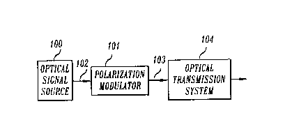
FIG. 1 is a simplified block diagram of an arrangement including
a polarization modulator which facilitates the practice of the invention;
- ~21738
- 3 -
FIG. 2 shows a view of the waveguide and electrode structure of one
arr~ngemPnt which may be employed for the po1qri7~tion mo~ tor of FIG. l;
FIG. 3 shows a view of still another waveguide and electrode structure
which can be utilized for the polarization modnl~tor of FIG. l; imd
S FIG. 4 shows a view of yet another waveguide and electrode structure
which can be advantageously utili_ed for the polari_ation mocl111~tc)r of FIG. l.
Detailed Desc . ;~Lion
FIG. 1 shows a ~imp!ifiP~l block diagram of an exemplary an~ng~mf,nt
fs~i1it~ting the practice of the i,.~,ntion. As shown, the invention includes
10 po1~ri7~tinn mo~lnl~tor l0l which is employed to mod11l~te the SOP of an optical
4~ 1 ;on signal from ~ptical signal source l00 to be supplied to optical
lla-~ n:~sion system 104. To this end, optical inr,. . . ~I;on signal 102 is 1~11r~hed
into po1~ri7~tion modul ~t~r l0l and the resulting mo~ul~ted optical hlr~ n
signal 103 is supplied to ~ iC~:~n system l04. Optical inforrn~tion signals suchlS as 102 are produced by a laser tr~n~mitt~.r (not shown) in optical signal source l00,
in well-known fashion. Specifi~11y, the pc~1~ri7~tion state of optical signal 102
being supplied to pol~ri7~ion ml d--l~tor 101 is such as to assure adequate
modul~tion through pairs of c,.li,ogonal po1~ri7~tion states.
FIG. 2 shows one e-.~ho~ e.~ of polari_ation mod1~ r l0l which
20 may be advanta~oue1y used in p~acticing the invention. An h.t~ ed optic
rea1i7~tion of po1 . ;,~ I ;o~- m~dul 101 is fabricated on low-bu~f.; .~g. - lce X-cut,
Zpropag~ting LiNbO3 Sul~Slluh 201 and operates with a standard titanium-
indi~used, single mode waveguide 202. It includes two electrodes 203 and 204
~1isrosed on sub~ tc 201 on both sides of waveguide 202.
The e-'.~] -.~f -1l of po1~ A~;on mt~dll1~tor l0l shown in F~G. 2
operates to retard the po1~ ihn co. . ~i~on~ n~ of the inroming optical signal 102
parallel to the X axis (TM mode) relative to the pol~ri7~tion co.l.ponf nl of the
i~cc~ g optical signal parallel to the Y axis (TE mode). The TE-TM mode phase
shift is induced via the r22 and r 12 (r22 =-r 12 = 3.4 ~ l0- 12 m/V) electro-opdc
30 cG~ i r.~ t~ by applying b -1~nred drive voltage co.-~ponents V(t) and -V(t) to
elecll.,des 203 and 204, thereby in~Cing an electric field Ey in ~.a-eE,uide 202. The
total induced phase shift ~(t) between the X and Y polarized co-nponcnls is
~(t) = r (rl2-r22) ~,, ~ V(t) ~ L nO (l)
where t is dme, ~ is the free-space wavelength, G is the gap between el~L.~des 203
35 and 204, L is the length of ele~ dcs 203 and 204, nO is the ordinary index of
2 L2173&
- 4 -
refraction and r is a n~ i7ed overlap pala~ t~, between the optical and electrical
fields.
The optical inforrnation signal 102 is lAnnrhed into waveguide 202 of
polari_ation modulator 101 having equal components of polarization along the X and
5 Y axes. Modulation of the drive voltages applied to two electrodes 203 and 204 then
causes the output polari~don state of the resulting mt~d~ t~l optical signal 103 to
move along a polar great circle on the Poincare' sphere. If the drive voltages V(t)
and -V(t) being applied to electrodes 203 and 204 are periodically mo-3ul~ted such
that the peak-to-peak voltage Amplitude induces a total phase shift ~(t) =~1, then
10 the SOP of output optical signA~ 103 is periodirAlly m~lllAtPd between two
orthogonal po1 ~ri7Ation states. If the peak-to-peak voltage amplitude being applied
to clec~od~s 203 and 204 is adjusted to induce a total phase shift of Q~(t) = 2~,
then the SOP of output optical signal 103 traces a full great circle on the Poincare'
sphere. In a p,er~ d e -~ho~ of the invention, the drive voltages applied to
lS clccl u~s 203 and 204 of pol?ri7Ation rnodl-l~tnr 101 A~re S~/mll~ClliC sawtooth
voltages of the form
V(t) =V,~ )n (4ft- 2n), for 2n-1 ~ 4ft S 2n+1, (2)
where t is dme, n is an arbitrary integer, l/f is the sawtooth period, and V,~ is the
voltage for inducing a phase shift of ~(t) = r~. Preferably, the rate of the SOP20 mr~lllAtion is at a rate suk~ n;Ally higher than 1/ tS~ where ts is the anisotropic
sPtn~Ation dme of the opdcal Amplifi~r ( typically 1 ms ).
In the example shown in FIG. 2, pr~lPri7Ation moclulAtrJr 101 operates to
mr~dlll- an inComin~ opdcal inÇ,~ ion signal 102 having a 45~ linear SOP
reladve to the X and Y axes. In lG;.l,onse to the ~y" ", ~- l ~ ;ral Sdw~OOIIl drive voltages
25 V(t) and -V(t), noted above, being applied to the modlllPt~-r electrodes 203 and 204,
respecdvely, the SOP of the optical signal 103 emerging as an output from
m~lll~tor 101 traces A SC 1~ 'et~ polar great circle on the Poincare' sphere and, then,
returns in the opposite direction to the point of beginning, as shown in FIG. 2. Thus,
in a steady state confliti~n, the SOP of optical signal 103 proceeds through the30 seq~e~c6 of polarization states shown, namely: 45~ linear, left circular, -45~ linear,
right circular, 45~ linear, right circular, -45~ linear, left circular, etc. It is noted that
the SOP of the optical inro. "~til~.~ signal 102 could be circular, if desired, or
ellirti~al with a ~ P~ axis ati45~. Then, the modl~ ion of the SOP of output
opdcal signal 103 will begin a~ a different point in the s~uencc, move all the way
3 8
around a great circle on the Poincare' sphere1 and then return along the great circle to
the point of ~eginning
If desired, balanced sinusoidal drive voltages could be employed to
provide the mocl~ tion, namely,
V(t) = Vm sin(2~ft) (3)
However, use of the $inncoid~1 drive voltages will cause the pol~ri~tion states to be
traced along a great circle on the Poincare' sphere with non-uniform speed. In the
case of Vm = V7~, the m~n~ f d optical signal 103 traces a full great circle on the
Poincare' sphere, but will spend unequal time intervals in the orthogonal pol~i7~tion
10 states. Nevertheless, different values of Vm~ causing inco~plctc or o~e.~;c ,':
great circles to be traced on the Poincare' sphere under sinllcoi~l~l drive voltages, can
also be used to equali_e PDHB effects through appropriate non-uniform weighting of
SOPs. The general re4ui,~nlellt is that Vm must be selected to cause the averagedegree of po1~ri7~tion to vanish over a sing1e mndnlstion cycle. In the case of
15 Vm = 0.7655 ~ V,~, for e Y~ p'~. the mnd111~tf~d optical signal 103 will trace only
76% of a full great circle on the Poincare' sphere, but optical signal 103 will, on
average, be cc.n~l~!vt,~ ly depolari_ed.
FIG. 3 shows another e n~bo ~ f -t of polari_adon mnd~ tnr 101 which
also may be ~ ,cd in pr~Gti--ing the invendon. Again, an int~dt~d optic
20 re~li7~tion of polo~i7~tion mod~ 101 is f~brirat~d on low-birPfrin~nce X-cut,
Z-p.vp~g. ~ing LiNbO3 s.lb~ te 201 and operates with a standard dtanium-
indilrused, single mode waveguide 202. It includes three cl_c~ odes, two of which,
i.e., 203 and 204, are ~3ispose~ on both sides of waveguide 202 and one cornmon
ground el~h~df~ 205 on the top of ~.a~ ,uide 202. This e-..bod;n.~ nt of mod11lotor
25 101 operates in a sirnilar fashion to an endlessly rotadng half-wave plate, i.e., it
g.,.,~ a constant phase retardadon of ~ at a variable orient~tion This is achieved
by infl1~çine a variable col~bi~tiol~ of TE-l~ll phase shifdng and TE ~ TM mode
con~vr~;on.
TE ~ TM mode conversion is accomplished via the r6l (r6l = -r~)
30 electro-opdc c~ rrlr f "~ by applying drive voltages V(t) and V' (t) to the side
ele~h~ies 203 and 204, thereby in(iucin~ an electric field E,~ in the waveguide 202.
The phase ret~qti~ n 11 (t) for mode CO -~ ;OIl induced in an electrode sectdon of
length L is
~l't'~l~7~8
- 6 -
~ (t) = r r6~ G) L n3 (4)
where t is time, ~ is the free-space wavelength, G is the gap between the groundelectrode 205 and the side ele~nl~es 203 and 204, L is the length of electrodes 203,
204 and 205, nO is the ordinary index of refraction and r is the spatial overlap of the
S applied electric field E,~ with the optic fields (0 5 r s 1).
TE-TM phase shifting is induced in a similar way as in the embodiment
of mor~ tor 101 shown in FIG. 2 by applying opposite drive voltages
V(t) = -V'(t) to side electrodes 203 and 204.
The drive voltage V(t) and V' (t) applied to electrodes 203 and 204,
10 respectively, are
V(t) =Vo sin(27cft) + Vncos(21~ft) + VT and (S)
V (t) =V0 sin(2~ft) -- V,~cos(2~ft) -- VT ' (6)
where V0 is the voltage that induces coll~lct~, TE-TM mode co.~ ;on (r~
V,~ is the voltage that induces a TE-TM phase shift of ~ ), and VT is the
15 voltage that reduces the residual, stadc birçfringpnce in waveguide 202 s~l~s~anti~lly
to _ero (0).
When driven by these drive voltages V (t) and V' (t), po1 - i7~ion
mo~ tor 101 acts like a rotating h_lf-wave plate spinning at a constant angular
velocity of 7~f.
In the example shown in FIG. 3, pols~i7ation n~Ul~a~tr~t 101 operates to
modlllate an in~.Qming optical h.r~ tion signal 102 being l~-~ncl~ed at a linearly
pol~i~4d state of arbitrary o~ t -~ relative to the X and Y axes. In l~t,on~ to
the drive voltages noted above, the SOP of the optical signal 103 emerging from
pr~ ;ZaliOn m~ 9tOr 101 traces the entire equatorial circle upon the Poincare'
25 sphere con~ u~usly in the same direction at a constant angular velocity of 2~f. The
periodic S~ u~cG of polpri7~tior~ states of the output optical signal 103 e..,~ ing
from the polarization modular is as shown in FIG. 3. Output optical signal 103 is
always linearly polarized and passes through the following sc~lucl1ce: 45~ linear, 0~
linear, -45~ linear, 90~ linear, 45~ linear and repeating itself. It is noted that the
30 pQ' ~ - l~ion state of the optical il.ÇJ- . n~f ion signal 102 can be arbitrary linear. The
pc'~ ~ion seCl~en~e of output optical signal 103 may then begin at a different state.
~d~lition~lly~ the pcl ;,~tio~ s~ue~ce of output optical signal 103 may also be
~. .. .
... ... . ~ ~ . .
. : ~
212~738
caused to pass through the above noted sequence in the opposite direcdon. The
tracing of the equatorial circle at a constant speed is realized here by employing
sin~lsoid~l drive voltages, which allow substantially higher modulation frequencies
than the sa~,vtooth voltages required in the embodiment of FIG. 2.
FIG. 4 shows another embodiment of polarization modulator 101, which
is particularly suited for high speed mo(~ 7.tion
The integrated-optic reali7~tion is fAbric~ted on (high-birefring~nce) Z-
cut LiNbO3 substrate 201 and operates with a standard titanium-indiffused, single-
mode u d~,guide 202. It includes three elecll des, two ground electrodes 203 and204 disposed on both sides of waveguide 202 and the drive electrode 205 on top of
waveguide 202. In this eY~mrle~ drive electrode 205 is tPrmin~tçd via resistor 206 to
electrode 204. This embo lim~nt of mnrll-lqtor 101 operates in a similar fashion to
the embodiment of FIG. 2, producing periodic TE-TM phase shifdng. The
modlll~tor in FIG. 4, however, udlizes suk~t~ lly higher r33 - rl3
(r33 - rl3 = 20 10-l2m/V) el~l-oo~lic coçffici~nt~ than the mtlcln' 101 of
FIG. 2 and can, ~h~ler(,lt, be driven with a su~st~nti~lly lower drive voltage
~mp!it~l~le Vn~ This, in turn, allows sllbst~ntislly higher modnl~-~inrl r~ u~,n~ies
than with the mo~lul~tor 101 of FIG. 2.
The m~lnl~t~r r~u~,ncy may be further hlcl-,ascd by using traveling
20 wave ele~l,vdes with a ~ inn resistor 206, i.e., by decigl~ing the el~l.~es, in a
well known fashion, to be part of the electrical ~ .n;SSion line pr~vidin~ the high-
r~uen~;y electric modl-l~tion signal.
The e .~ nt shown in PIG. 4 is particularly suited for moc~ tin~
the SOP of the OUtpllt opdcat signal 103 at a rlequcllcy which is a se1ected muldple
25 of the i,.rO. .n -liol- signal clock. This, in turn, tends to reduce the effects of
pol~i7~tion de~ Af,~-t loss.
The above-descTibed ~n~,. ..~nl~ are, of course, merely illustrative of
tho appli~t;on of the p- ;~;pks of the invendon. Other arrnng~m~t~ may be
devised by those skilled in the art without departing from the spirit or scope of the
30 invention. It should further be understood by those skilled in the art that although a
dtanium-indiffused w a~guide structure for a lithium niobate modlll~tor is the
preferred design, other waveguide formadons are contemrl~ted and other ~ulJsllates
may be elll~lo~ed inrl~l-ling but not limited to semiccn(luctor m~t~.ri~l5 and lithium
t~ntal . for o - . 'e Although not specific~lly shown, it is to be und,.~t~od that
35 opdcal signal source 100 includes means for obt~ g the desired potc ;"-lio ~ of the
optical signal being supplied to po~ ol~ m~ tor 101. A~ til -'ly, the
3 8
mod~ çd optical signal 103 is typically l~llnch~d from the m~\ll~t~-r 101 to theoptical tr~n~mi~ion system 104 via an ~mrlifi~ ion stage or the like.