Note : Les descriptions sont présentées dans la langue officielle dans laquelle elles ont été soumises.
TITLE
ADHESIVE SHEET FOR WAFER AND PROCESS
FOR PREPARING SEMICONDUCTOR APPARATUS USING THE SAME
FIELD OF THE INVENTION
'the present invention relates to an adhesive sheet for
a semiconductor wafer (referred to as "wafer" hereinafter)
and a process far preparing a semiconductor device using
this adhesive sheet. More particularly, the invention
1O relates t o an adhesive sheet which is used for applying and
fixing thereon a wafer having been subjected to wafer
processing in order to dice 'the wafer into element chips
(referred to as °'chips" hereinafter) in a process for
preparing a semiconductor device having such a structure
that the back surfaces of the chips are partially or wholly
in contact with a package molding resin (sealing resin),
and the invention also relates to a process for preparing a
semiconductor device using this adhesive sheet.
Z O BACKGROUND OF THE INVENTION
With higher integration of memories, there have
recently been made a variety of requests to semiconductor
device by users, for example, high speed response,
reduction of electric power consumption, widening of output
2 5 word structure ahd enlargement of package variation. For
coping with these various requests, package designing
should be made flexibly.
2
I.n order to satisfy the above-mentioned requests,
semiconductor devices of LOC (Lead On Chip) structure have
been proposed, as described in for example "Nikkei
Microdevices" (pp. $9-97, February, 1991) and Japanese
Patent Laid-Open Publication No. 246125/1990. The LOC
structure has various advantages such as minimized size,
high speed response, reduced noise and easy layout, and
hence it is said that the LOC structure is most strikingly
adopted to large-scale semiconductor devices which are
expected to be developed in future.
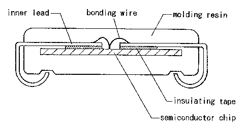
In 'the LOC structure, as shown in Fig. 7, plural inner
leads of a semiconductor device lead frame (referred to as
"lead frame" hereinafter) are fixed onto a surface of a
chip, on which a circuit has been formed, by way of
insulating tapes which electrically insulate the inner
leads from the chip, and the inner leads are electrically
connected with the chip by a bonding wire. The
semiconductor device is sealed with a molding resin, and
the back surface of the chip is in contact with the molding
resin.
The LOC structure has various advantages as described
above, but this structure involves problems which must be
solved because it is entirely different from structures of
conventional packages. One of problems which must be
2 5 solved is lowering of reliability caused by separation
between the chips and the molding resin, occurrence of
package cracks, etc.
~:1.2~2~~8
3
The lowering of reliability caused by occurrence of
package cracks, etc. is not an inherent problem in the
semiconductor device having the LOC structure, and it is a
very serious problem to all the semiconductor devices
having such structures as shown in Figs. 8 to 9 wherein the
back surface of the chip is partially or wholly in contact
with the molding resin. Fig. 8 shows a serniconductor
device having such a structure that a die pad has a slit.
Fig. 9 shows a semiconductor device having a COL (Chip On
Lead) structure.
The mechanism of the separation between the chips and
the molding resin or the occurrence of package cracks has
been diversely reported so far.
One of the mechanism of these phenomena is an invasion
of moisture into the IC package.
The invasion routes of moisture into the IC package
are broadly classified as follows:
(1) invasion through interface between the lead frame
and the resin,
2 0 (2) invasion through interface between the resin and a
filler filled in the resin, and
(3) invasion through the resin bulk.
These invasions are caused by capillarity or
diffusion, and as the environmental temperature or humidity
2 5 at which the IC package is left rises, the IC package
absorbs moisture more easily. Further, as the
environmental 'temperature rises, the moisture diffusion
rate at the initial stage becomes higher and the moisture
absorption reaches its saturation point more rapidly. For
example, there i.s a report that when the IC package is
allowed to stand at 85 °C and 85 oRH (RH: relative
humidity) and to absorb moisture, the moisture absorption
reaches 80 to 90 0 of its saturation point in about 168
hours. Moreover, even in an ordinary atmosphere of an
ordinary temperature and 75 ~FtH, moisture easily permeates
the molding resin material of. the IC package, for. example,
an epoxy resin.
In the IC package such as SOJ or QFP, soldering is
conducted generally by means of IR reflowing in which
heating is effected by infrared rays or vapor reflowing in
which an inert liquid is vaporized and the IC package is
exposed to the ~rapor of high temperature since both
reflowing methods are suitable for mass production. In the
IR reflowing, the former method,'the IC package is exposed
to a high temperature of 290 to 250 °C, whereby the
moisture which has invaded inside of the IC package as
2 0 described above is explosively expanded by 'the high
temperature during the reflowing operation, and thereby
water vapor pressure is appl9.ed onto the interface between
the epoxy resin and 'the lead frame to bring about
interfacial separation therebetween. As a result, package
cracks take place.
The package cracks caused by the IR reflowing are
often observed even when the package is allowed to stand at
~1222~~
an ordinary temperature for about 16$ hours, though it
depends on the shape of the lead frame in the package, the
surface area of the chips, etc.
One reason for promoting the interfacial separation is
S a decrease of adhesion strength between the resin material
used for sealing the package, for example, an epoxy resin,
and the contact surface of the chip. The adhesion strength
is largely influenced by cleanliness of the adherend
surface. For example, the adhesion strength is very
sensitive even to a foreign substance having an angstrom
level thickness remaining on the adherend surface so as to
decrease the adhesion strength, whereby invasion of
moisture or retention thereof within the package is easily
made, and finally the package cracks are brought about.
By the way, semiconductor wafers of silicon, gallium-
arsenide, etc. are usually produced in relatively large
diameter, and the wafers are diced into chips, which are
then transferred to the subsequent mounting stage. At this
time, the semiconductor wafers are subjected to such
2 0 operations as dicing, rinsing, drying and irradiation of
radiation rays to cure the radiation curing adhesive layer
of an adhesive sheet in a state that the semiconductor
wafers are adhered to the adhesive sheet. Then, an
expansion operation of the adhesive sheet is carried out if
necessary, and thereafter operations of picking up the
chips and mounting the chips are carried out.
G
Adhesive sheets which are intended for use in the
processing stages of wafers, from the dicing stage up to
the pick-up stage, are desired to have an adhesion force
sufficient to retain wafers and/or chips thereon in the
course from the dicing stage up to the expanding stage, but
in the pick-up stage, they are desired to only retain an
adhesion force of such an extent that no adhesive remains
on the picked-up wafer chips. As such adhesive sheets for
applying wafers thereon as mentioned above, those described
1 0 in for example Japanese Patent Publication No. 56112/19$9
have been generally used, and -they can be used without any
problem in preparing semiconductor devices of conventional
type.
However, in the preparation of semiconductor devices
having such a structure that 'the back surfaces of the chips
are partially or wholly in contact with the molding resin,
a trouble of package crack occurrence is observed and the
reliability of the semiconductor.device is reduced.
2 0 OBJF~T OF THE INVENTION
The present invention has been made in the light of
the foregoing techniques in the prior art, and it is an
object of the present invention to provide an adhesive
sheet for wafer (referred to as "adhesive sheet for wafer"
hereinafter) which is used in preparing a semiconductor
device having such a structure that the back surfaces of
chips are parti.all.y or wholly in contact with a molding
.--..
~~.~?~~"~3
resin and which can prevent occurrence of package cracks
thereby to enhance reliability of the semiconductor device.
It is another object of the present invention to provide a
process for preparing a semiconductor device using this
adhesive sheet.
S~1MMARY QF THE INVENTION
The adhesive sheet for wafer according to the present
invention is an adhesive sheet comprising a substrate film
1 0 and a radiation curable adhesive layer formed thereon, said
adhesive sheet being used in a process for preparing a
semiconductor device comprising the steps of adhering a
back surface of a wafer, a front surface of which has been
formed a circuit, onto the radiation curable adhesive
layer, dicing the wafer into chips, irradiating the
radiation curable adhesive layer with radiation to cure
said adhesive layer, expanding the adhesive sheet if
necessary to make the chips apart from each other, then
picking up the chips, mounting the chips on a lead frame,
2 0 bonding, and molding (sealing) to give such a structure
that the back surfaces of the chips are partially or wholly
in contact with a package molding resin,
wherein the radiation curable adhesive layer comprises
100 parts by weight of an acrylic adhesive composed of
a copolymer of an acrylic ester and an OH group-containing
polymerizable rnonomer and
50 - 200 parts 1>y weight of a radiation polymerizable
compound having two or more unsaturated bonds, and
the radiation curable adhesive layer has an elastic
modules of not less than 1 x 10⁹ dyn/cmz after curing by
irradiation with radiation.
The process for preparing a semiconductor device
according to the present invention uses an adhesive sheet
for wafer comprising a substrate film and a radiation
curable ahdesive layer provided thereon which comprises 100
parts by weight of an acrylic adhesive composed of a
copolymer of an acrylic ester and an OH group-containing
polymerizable monomer and 50 - 200 parts by weight of a
radiation polymerizable compound having. two or more
unsaturated bonds and has an elastic modules of not less
1 5 than 1 x 10⁹ dyn/cm2 after curing by irradiation with
radiation, and the process comprises the steps of adhering
a back surface of a wafer, a front surface of which has
been formed a circuit, onto the radiation curable adhesive
layer, dicing the wafer into chips, irradiating the
2 0 radiation curable adhesive layer with radiation to cure
said adhesive layer, expanding the adhesive sheet if
necessary to make the chips apart from each other, then
picking up the chips, mounting the chips on a lead frame,
bonding, and molding (sealing) to give such a structure
2 5 that the back surfaces of the chips are partially or wholly
in contact with a package molding resin.
2~~~~~
In the present invention, it is preferred that 20 to
80'~ by weight of a radiation polymerizable compound having
two or more unsaturated bonds are those having four or more
unsaturated bonds.
BRIEF DESCRIPTION OF THE DRAWING
Fig. 1 is a schematic sectional view of an
adhesive
sheet wafer according to the present invention.
for
Fig. 2 is a schematic sectional view of another
adhesive
sheet
for wafer
according
to the
present
invention.
Fig. 3 is an illustration showing a state where
a
wafer applied onto an adhesive sheet for wafer.
is
Fig. 4 is an illustration showing a state where
a
1J' wafer diced into chips, an adhesive sheet is
is expanded
and the heet is irradiated with radiation.
s
Fig. 5 is an illustration showing another pick-up
stage chips.
of
Fig. 6 is an illustration showing another pick-up
2 0 stage chips.
of
Fig. 7 is a sectional view of a semiconductor
device
having L0C structure.
a
Fig. 8 is a sectional view of a semiconductor
device
having ch a structure that a die pad has a slit.
su
2S Fig. 9 is a,sectional view of a semiconductor
device
having COL (Chip On Lead) structure.
a
2~.2~~~~~
io
DE'I'AILEU DESCRIPTION Of THfE INVENTION
The adhesive sheet for wafer and the process for
preparing a semiconductor device using the adhesive sheet
according to the present invention are described in detail
hereinafter.
As shown in Figs. 1 to 6, the adhesive sheet for wafer.
1 of the present invention comprises a substrate film 2 and
a radiation curable adhesive layer 3 provided thereon. The
adhesive sheet 1 is used in preparing a semiconductor
device having such a structure that the back surfaces of
chips are partially or wholly in contact with a molding
resin. This process comprises the steps of adhering a
wafer A which has been subjected to wafer processing onto
the radiation curable adhesive layer 3, dicing the wafer in
5 this state into plural chips, rinsing, drying, irradiating
the radiation curable adhesive layer 3 of the adhesive
sheet 1 with radiation to cure the adhesive layer so as to
decrease the adhesion force of the layer, expanding the
adhesive sheet if necessary to make the chips apart from
2 0 each other, then picking up the chips from the radiation
curable adhesive layer 3, mounting the picked chips on a
given support substrate, for example, a lead frame, and
finally molding with a resin.
As can be seen from its sectional view shown in Fig.
~5 1, the adhesive sheet for wafer 1 of the invention
comprises the substrate film 2 and the radiation curable
adhesive layer 3 provided on the surface of the substrate
m
film. Before the use of this adhesive sheet, it is
preferred to temporarily apply a release sheet 9 onto the
radiation curable adhesive layer 3 to protect the adhesive
layer 3, as shown in Fig. 2.
The adhesive sheet for wafer 1 of the invention may be
shaped into any form such as tape-like, label-like or other
form. Suitable as the substrate :film 2 are rnaterials which
are excellent in water resistance and heat resistance, and
on this 'view, synthetic resin films are particularly
1 0 suitable. As will be stated later, the adhesive sheet for
wafer of the invention is irradiated with radiation such as
electron beam (EB) or ultraviolet light (UV), and the
substrate film 2 is not required to be transparent when the
adhesive sheet is subjected to EB irradiation but must be
transparent even though colored when the adhesive sheet is
subjected to UV irradiation.
Employable as the substrate film 2 axe films of
synthetic resins such as polyethylene, polypropylene,
polyvinyl chloride, polyethylene t erephthalate,
2 0 polybutylene terephthalate, polybutene, polybutadiene,
polyurethane, polymethylpentene, ethylene/vinyl acetate
copolymer, ethylene/(meth)acrylic acid copolymer,
ethylene/methyl (meth)acrylate copolymer, ethylene/ethyl
(meth)acrylate copolymer, etc. A laminate of these films
2 5 is also employable. The thickness of 'the substrate filrn 2
is usually in the range of about 10 to 300 Elm, preferably
50 to 200 Etm.
a z ~:~.2~~'~8
In the case where the adhesive sheet needs to be
subjected to an expansion treatment after the dicing of
wafer, a synthetic resin film having extensibility in the
lengthwise direction and the crosswise direction, such as a
film of polyvinyl chloride o.r a film of polyethylene
conventionally used, is preferably used as the substrate
film.
The adhesive sheet for wafer 1 of the present
invention comprises the substrate film 2 described above
and a radiation curable adhesive layer 3 formed on the
substrate film 2. The radiation curable adhesive layer 3
has an elastic modules of not less than 1 x 10⁹ dyn/cmz,
preferably 1 x 10⁹ to 1 x 101° dyn/cmz, after curing by
irradiation with radiation.
1~ The elastic modules mentioned herein is determined in
the following manner. That is, a small specimen of an
adhesive which forms the adhesive layer 3 having a length
of 50 mm, a width of 9 mm and a thickness of 0.2 mm is
prepared. The specimen is placed under a high-pressure
2 0 mercury lamp of 80 W/cm and irradiated with radiation for 1
second to cure it. After curing, the specimen is measured
on the elastic modules at 3.5 Hz by means of a
viscoelasticity measuring device (Rheovibron DDV-II-FP,
produced by Orientic K.K.) to obtain a graph of elastic
z5 modules, and from the graph a value at 25 °C is sought as
the elastic modules of the adhesive layer.
13
The radiation curable adhesive layer 3 formed on the
substrate film 2 comprises an adhesive and a .radiation
polymerizable compound. Suitable as the adhesive are
acrylic adhesives composed of a copolymer of an acrylic
ester and an OH group-containing polymerizable monomer.
The acrylic adhesives are copolymers containing repeating
units derived from acrylic esters and repeating units
derived from OH group-containing polymerizable monomers as
its principal constituent units. The OH group-containing
polymerizable monomer units are contained in the copolymer
in an amount of 0.5 to 30 o by mol, preferably 8 to 30 o by
mol, more preferably 20 'to 30 o by mol.
Examples of the acrylic esters suitably used include
acrylic esters of alkyl alcohols having 1 to 10 carbon
atoms and methacrylic esters of alkyl alcohols having 1 to
10 carbon atoms.
Examples of the OH group-containing monomers suitably
used include 2-hydroxyethyl acrylate, 2-hydroxyethyl
methacrylate, hydroxypropyl acrylate and hydroxypropyl
2 0 methacrylate. Of these, 2-hydroxyethyl acrylate and 2-
hydroxyethyl methacrylate are preferred.
The copolymer obtained by copolymerizing these
monomers has a molecular weight of 1.0 x 10⁵ to 10.0 x 10⁵,
preferably 4.0 x 10⁵ to $.0 X 105.
2 S In addition~to the above-mentioned constituent units,
the acrylic adhesives may contain other constituent units
such as those derived from vinyl acetate, acrylonitrile,
[ ~ ~~~2~~~
vinyl alkyl ether, etc., provided that the object of the
present invention is not marred.
The adhesion force and the cohesion force of the
acrylic adhesives can be optionally determined by 'the use
of a crosslinking agent. Examples of the crosslinking
agents include polyvalent isocyanate compounds, polyvalent
epoxy compounds, polyvalent aziridine compounds and chelate
compounds. Concrete examples of the polyvalent isocyanate
compounds include tolylene diisocyanate, diphenylmethane
diisoCyanate, hexamethylene diisocyanate, i.sophorone .
diisocyanate and adducts thereof. Concrete examples of the
polyvalent epoxy compounds include ethylene glycol
diglycidyl ether and diglycidyl terephthalate. Concrete
examples of the polyvalent aziridine compounds include
tris-2,9,6-(1-aziridinyl)-1,3,5-triazine, tris(1-(2-
rnethyl)-azir:idinyl]phosphine oxide and hexa[1-(2-methyl)-
aziridinyl)triphosphatriazi.ne. Concrete examples of the
chelate compounds include ethyl acetoacetate aluminum
diisopropylate and aluminum tris(ethylacetoacetate).
2 0 As the radiation polymerizable compound for the
radiation curable adhesive layer. 3, there can be widely
used low-molecular weight compounds having at least two
photopolymerizable carbon-carbon double bonds in the
molecule capable of forming a three-dimensional network
upon light irradiation, as described.in for example
Japanese Patent Laid-Open Publications No. 196956/1985 and
No. 223139/1985. Concrete examples.of such low-molecular
i s ~~.~~2'~~
weight compounds include trimethylolpropane triacrylate,
tetramethylolmethane tetraacrylate, pentaerythritol
triacrylate, pentaerythritol tetraacrylate,
dipentaerythritol monohydroxypentaacrylate,
s dipentaerythritol hexaacrylate, 1,9-butylene glycol
diacrylate, 1,6-hexanediol. diacrylate, polyethylene glycoa.
diacrylate and commercially available oligoester acrylates.
In addition to the acrylate compounds as mentioned
above, urethane acrylate oligomers are also employable as
the radiation polymerizable compound. The urethane
acrylate oligomers may be prepared by reacting polyester or
polyether type polyol compounds with polyvalent isocyanate
compounds, for example, 2,A-tolylene diisocyant e, 2,6-
tolylene diisocyante, 1,3-xylene diisocyanate, 1,4-xylylene
1$ diisocyanate and diphenylmethane-9,9-diisocyanate, to
obtain isocyanate urethane prepolymers which are then
reacted with acrylates or methacylates having a hydroxyl
group, for example, 2-hydroxyethyl acrylate, 2-hydroxyethyl
methacrylate, 2-hydroxypropyl acrylate, 2--hydroxypropyl
2 0 methacrylate, polyethylene glycol acrylate and polyethylene
glycol methacrylate.
Of such urethane acrylate oligomers, those having a
molecular weight of 3,000 to 30,000, preferably 3,000 to
10,000, more preferably 4,000 to 8,000, are particularly
2s preferably used because the adhesive containing these
urethane acrylate oligomers does not adhere to the back
surface of the chips in the pick-up .stage of the chips even
2~,2~2'~~
16 '
if the back surface of the wafer is rough. Further, the
urethane acrylate oligomers preferably have at least two
carbon-carbon double bonds, more preferably two carbon-
carbon double bonds (namely 2-functional). Furthermore, in
the case of using the urethane acrylate oligomers as the
radiation polymerizable compound, there can be obtained an
extremely excellent adhesive sheet, as compared with the
case of using only the low-molecular weight compound having
at least two photopolymerizable carbon-carbon double bonds
1 ~ in the molecule as disclosed in Japanese Patent Laid-Open,
Publication No. 196956/1985. In other words, the obtained
adhesive sheet has a sufficiently high adhesion force
before irradiation with radiation, but after the
irradiation the adhesion force of the sheet decreases to
15 such a level that no adhesive remains on the back surfaces
of the chips in the pick-up stage of the chips.
In the present invention, it is preferred to use a
plurality of the radiation polymerizable compounds in
combination. For example, it is desirable that about 20 to
2 0 80 ~ by weight, preferably about 30 to 70 o by weight of a
radiation polymerizable compound having two or more
unsaturated bonds are those having four or more unsaturated
bonds. Concrete examples of the radiation polymerizable
compound having four or more unsaturated bonds include
2 5 pentaerythritol tetraacrylate,
1,6-bis(glyceryl urethane)hexane tetramethacrylate
(1),
z~ ~:~2~2'~~
~H3 ~H3
(CH2 CCOOCH~)2CHOCONH-C6H12 NHCOOCH(CH20COC=CHZ)2 '~'(1)
bis(glyceryl urethane)isophorone tetramethacrylate
(2) , and
iH3 CH3 CH3 ..
. . (CH2 CCOOCH2)2CHOCOIVH- CH2 NHCOOCH(CH20CDC=CHZ)2 .. . . (2)
~0
CH3 CHg
bis(glyceryl urethane)toluene tetramethacrylate (3). .
iH3 iH3
~ 5 (CH2=CC00CH2)2CHOCONH ~ NHCOOCH(CH20COC=CH2)2 ~ ~ ~ (3)
. . CH 3
When such radiation polymerizable compound havin.g:four
or more unsaturated bonds is used in an amount of 20'to 80
2 0 % by weight based on 100 0 of the radiation polymerizable
compound, the radiation curable adhesive layer is
sufficiently cured by irradiation with radiation and the
cohesion fbrce of. the adhesive does not decrease.
Further, it is particularly preferred that the
2 5 radiation polymerizable compounds having two or more
unsaturated bonds are used in combination with each other
wherein 20 to 80 o by weight, preferably 30 to 70 øa by
~~.2~~'~~
weight of those having four or more unsaturated bonds and
20 to 60 o by weight, preferably 30 to 50 o by weight of
those having six or more unsaturated bonds are present in
the total amount of the radiation polymerizable compounds
having two or more unsaturated bonds. Concrete examples of
the radiation polymerizable compound having six or more
unsaturated bonds include
dipentaerythritol hexaacrylate,
dipentaerythritol hexamethacrylate,
1,6-bis(pentaerythritol urethane)hexane hexaacrylate
(4) ,
(CHZ CH-C00CH2)3CCH20CONH-CsHl2 NHCOOCH2C(CH20COCH=CH2)3 .. . (4)
bis(pentaerythritol urethane)isophorone hexaacrylate
(5), and
CHs , , .
' ,:
(CH2 CH-C00CH2) 3CCHZOCONH ~ ~ CH2-NHCOOCH2C(CH20COCH=CHZ) 3 ..
' . . . (5)
C~I3 CH 3
bis(pentaerythritol urethane)toluene hexaacrylate (6).
(CHI=CH-COOCH2)3CCHZOCONH ~ CH2 NHCOOCHZC(CH20COCH=CH2)3
~ - ° ~' ... (6>
CH 3
m ~~~~~"~~
Examples of combinations of the radiation
pol.ymerizable compounds particularly preferably,used are
given below, but combinations employable in the present
invention are in no way limited to those examples.
1. A combination of 2-functional urethane acrylate
oligomer and pentaerythritol tetraacrylate which is 9-
functional.
2. A combination of 2-functional urethane acrylate
oligomer and dipentaerythritol hexaacrylate which is 6-
functional.
3. A combination of 2-functional urethane acrylate
oligomer and bis(petnaerythritol urethane)hexane
hexaacrylate.
With respect to the proportion between the acrylic
adhesive and the radiation polymerizable compound in the
adhesive layer, the radiation polymerizable compound is
used usually in an amount of 50 to 200 parts by weight,
preferably 50 to 150 parts by weight, particularly
preferably 70 to 120 parts by weight, based on 100 parts by
2 0 weight of the acrylic adhesive. The adhesive sheet
containing the acrylic adhesive and the radiation
polymerizable compound in such proportions has high initial
adhesion force, and moreover, the initial adhesion force
greatly decreases after irradiation with radiation and
hence the chips can readily be picked up from the adhesive
sheet.
20 .2~.~2~~8
If the amount of the radiation polymerizable compound
is less than 50 parts by weight, a large amount of the
adhesive may adhere to the back surfaces of the chips after
the compound is cured by irradiation with radiation,
whereby package crackings occur when the package is sealed
with a resin. On the other hand, if the amount of the
radiation polymerizable compound is larger than 200 parts
by weight, the cohesion force of the adhesive lowers to
induce another problem (i.e., separation of the adhesive
sheet from the frame), though occurrence of the package
crack can be inhibited.
The adhesive sheet for wafer 1 comprising the
substrate film 2 and the radiation curable adhesive layer 3
as described above has a sufficient adhesion force to the
adherend before irradiation with radiation but is markedly
decreased in the adhesion force after the irradiation with
radiation. More specifically, before irradiation with
radiation, the adhesive sheet has an adhesion force of, for
example, not less than 200 g/25 mm to a stainless steel
2 0 having been subjected to mirror surface treatment, but the
adhesion force decreases to not more than 20 g/25 mm after
irradiation with radiation.
The radiation curable adhesive layer 3 may contain, if
necessary, a radiation color developable compound (compound
which develops color upon irradiation), in addition to the
above-mentioned adhesive and radiation polymerizable
compound. By virtue of incorporating the radiation color
2] 2~~~~"~~
developable compound into the radiation curable adhesive
layer 3, the adhesive sheet is colored after irradiated
with radiation, whereby the detection accuracy is enhanced
at the time of detecting chips by means of a photosensor
and a possible failure in operation to pick up the chips is
prevented. Further, there can be obtained such an
advantage that whether the adhesive sheet has been
irradiated with radiation or not can be immediately
confirmed visually.
The radiation color developable compounds are
compounds which are colorless or pale-colored before
irradiation but develop color upon irradiation, and
preferred examples of such compounds are leuco dyes.
Preferably employable as the leuco dyes are those
conventionally used, such as triphenylmethane type, fluoran
type, phenothiazine type, auramine type and spiropyrane
type dyes. Concrete examples of~these dyes include 3-[N-
(p-tolylamino)]-7-anilinofluoran, 3-(N-(p-tolyl)-N-
methylamino]-7-anilinofluoran, 3-[N-(p-tolyl)-N-
2 0 ethylamino]-7-anilinofluoran, 3-diethylamino-6-methyl-7-
anilinofluoran, crystal violet lactone, 4,4',9"-
trisdimethylaminotriphenylmethanol and 9,4',9"-
trisdimethylaminotriphenylmethane.
Developers preferably used in combination with the
above-mentioned leuco dyes are those conventionally used,
such as initial polymers of phenol-formalin resin, aromatic
carboxylic acid derivatives and electron acceptors,'e.g.,
P
22
activated clay. In order to change the color tone, various
known color formers can also be used in combination
therewith.
The radiation color developable compound may be
incorporated into the radiation curable adhesive layer in
the form of a solution in an organic solvent or in the form
of fine particles. The amount of the compound to be
incorporated into the radiation curable adhesive layer is
usually in the range of 0.01 to 10 o by weight, preferably
0.5 to 5 a by weight. 2f the amount thereof exceeds 10 0
by weight, the radiation with which the adhesive sheet is
irradiated is too much absorbed by the compound, and hence
the radiation curing adhesive layer sometimes is cured
insufficiently. On the other hand, if the amount of the
compound is less than 0.01 o by weight, the adhesive sheet
is not sufficiently colored at the time of irradiation, and
hence a failure .in operation to pick up the chips easily
occurs
Under certain circumstances, the radiation curable
2 0 adhesive layer 3 may contain a powder of a light scattering
inorganic compound, in addition to the aforementioned
adhesive a'nd radiation polymerizable compound. By virtue
of incorporating the light scattering inorganic compound
powder into the radiation curable adhesive layer 3, even
when an adherend~susface of a wafer has been greyed or
blackened for some reason or other, the adhesion force of
the adhesive layer sufficiently decreases even at the
--,
23
portions corresponding to the greyed or blackened portions
of the wafer surface by irradiation of radiation such as
ultraviolet light, and hence no adhesive remains on the
back surfaces of the chips during the pick-up stage of the
chips, while the adhesive layer has a sufficient adhesion
force before irradiation.
The light scattering inorganic compounds referred to
above are such compounds as capable of irregularly
reflecting radiation such as ultraviolet light (UV) or.
1 0 electron beam (EB) when the compounds are irradiated with
such radiation. Concrete examples of the light scattering
inorganic compound powder include silica powder, alumina
powder, silica alumina powder, and mica powder. As the
light scattering inorganic compounds, those which almost
l~ perfectly reflect such radiation as mentioned above are
preferably employed, but those which absorb the radiation
to a certain extent are also employable.
The light scattering inorganic compound preferably is
in the form of powder, and has a particle diameter of 1 to
2 0 100 ~,m, preferably about 1 to 20 ~.m. In the radiation
curable adhesive layer, the light scattering inorganic
compound i~s desirably used in an amount of 0.1 to 10 o by
weight, preferably 1 to 9 o by weight. If the light
scattering inorganic compound is used in the radiation
2 5 curable adhesive~layer.in an amount exceeding 10 4 by
weight, the adhesion force of the radiation curable
adhesive layer sometimes decreases. .On the other hand, if
~~ . 2.~~~~ ~ ~
this compound is used in an amount less than 0.1 % by
weight, the adhesive layer is not sufficiently decreased in
the adhesion force after irradiation in the portions of the
adhesive layer corresponding to the greyed or blackened
portions of the wafer surface, and hence, the adhesive may
adhere to and remain on the back surfaces of the chips in
the pick-up stage of the chips.
As stated above, by the use of the adhesive sheet
comprising the radiation curable adhesive layer which
contains the light scattering inorganic compound powder,
even when the adherend surface of the wafer has been greyed
or blackened for some reason or other, the adhesion force
of the adhesive layer sufficiently decreases even at the
portions corresponding to the greyed or blackened portions
of the wafer surface by irradiation with radiation. The
reason for this is considered to be as follows. That is,
the adhesive sheet 1 of the present invention has the
radiation curable adhesive layer 3, and when this radiation
curable adhesive layer 3 is irradiated with radiation, the
2 0 radiation polymerizable compound contained in the adhesive
layer 3 is cured to decrease the adhesion force of the
adhesive layer. However, the wafer surface sometimes has
portions greyed or blackened for some reason or other.
When the radiation curable adhesive layer 3 is irradiated
with radiation, the radiation passes through the radiation
curable adhesion layer 3 to reach the wafer surface.
However, if the wafer surface has greyed or blackened
portions, the radiation is absorbed by those portions and
is not reflected. Therefore, the radiation which is to be
utilized to cure the radiation curable adhesive layer 3 is
absorbed by the portions corresponding to the greyed or
blackened portions of the wafer surface, and hence the
curing of the radiation curable adhesive layer 3 becomes
insufficient and, the adhesion force of the adhesive layer
does not sufficiently decrease. Accordingly, it is
considered that the adhesive adheres to and remains on the
1 0 back surfaces of the chips in the pick-up stage of the
chips.
However, when the light scattering inorganic compound
powder is incorporated into the radiation curable adhesive
layer 3, the radiation is irregularly reflected by the
compound and is altered in its direction before reaching
the wafer surface. On that account, even if greyed or
blackened portions are present on the wafer surface, the
irregularly reflected radiation sufficiently permeates into
the upper region of portions of the adhesive layer
2 a corresponding to the greyed or blackened portions of the
wafer surface and accordingly the corresponding portions of
the adhesive layer are cured sufficiently. By virtue of
incorporation of the light scattering inorganic compound
powder into the radiation curable adhesive layer, even when
2 ~ greyed or blanked portions are present on the wafer surface
for some reason or other, the curing of the adhesive layer
does not become insufficient at its.portions corresponding
26
~:~.~2~~"l ~
to the greyed or blackened portions of the wafer s~rrface
and accordingly no adhesive adheres to and remains on the
back surfaces of the chips in the pick-up stage of the
chips.
In the present invention, abrasive grains may be
dispersed in the substrate film. The abrasive grains have
a grain diameter of 0.5 to 100 elm, preferably 1 to 50 Elm,
and a Mohs hardness of 6 to 10, preferably 7 to 10..
Concrete examples of the abrasive grains include green
carborundurn, artificial corundum, optical emery, white
alundum, boron carbide, chromium(III) oxide, cerium oxide
and diamond powder. These abrasive grains preferably are
colorless or white-colored. The abrasive grains are used
in an amount of 0.5 to 70 o by weight, preferably 5 to 50 0
by weight, in the substrate film 2. Use of the abrasive
grains is particularly preferred when a dicing blade is
used in such a manner that the blade reaches up to the
substrate film 2 passing through the wafer.
By incorporating the abrasive grains into the
2 0 substrate film, even if the dicing blade comes .into the
substrate film and the adhesive sticks to the blade, the
adhesive can be easily removed owing to the abrasion effect
of the abrasive grains.
Further, the above-mentioned adhesive layer may
2 5 contain an UV curing initiator when the adhesive layer is
cured by UV irradiation, in order to shorten the
?7
polymerization curing time by UV irradiation and to
minimize the UV irradiation dose.
Concrete examples of such UV curing initiators include
benzoin, benzoin methyl ether, benzoin ethyl ether, benzoin
isopropyl ether, benzyldiphenyl sulfide, tetramethylthiuram
monosulfide, azobisisobutyronitrile, dibenzyl, diacetyl and
-chloroanthraquinone.
In the process for preparing a semiconductor device
according to the present invention, onto the adhesive sheet
for wafer as mentioned above is applied a semiconductor
wafer which has been subjected to wafer processing, then
the wafer is diced in this state into chips, from which a
semiconductor device i.s prepared.
The process for preparing a semiconductor device using
the above~mentioned adhesive sheet for wafer according to
the present invention is illustrated below.
In the case where a release sheet 9 is provided on the
adhesive sheet 1 as shown in Fig. 2, the release sheet 4 is
first removed, and the adhesive sheet 1 is placed so that
2 0 the radiation curable adhesive layer 3 looks upward. Onto
the surface of the radiation curable adhesive layer 3, a
wafer A which is to be diced is applied, as shown in Fig.
3. The wafer A is then subjected in this state to
operations of dicing, and if necessary, rinsing and drying.
2 S In that case, the wafer chips will not fall off from the
adhesive sheet 1 during each operation of dicing, rinsing
and drying because the wafer chips are sufficiently adhered
W A M IvJ FI 1 lJ
28
to and held on the adhesive sheet 1 by means of the
radiation curable adhesive layer 3.
Subsequently, the wafer chips are picked up from the
adhesive sheet and mounted on a support substrate, for
example, a lead .frame. As shown in Fig. 4, prior to or
simultaneously with the pick-up operation, the radiation
curable adhesive layer 3 of the adhesive sheet 1 is
irradiated with an ionizing radiation B such as ultraviolet
light (UV) or electron beam (EB) to polymerize and cure 'the
1 0 radiation polymerizable compound contained in the radiation
curable adhesive layer 3. When the radiation polymerizable
compound contained in the radiation curable adhesive layer
3 is polymerized and cured by irradiating the adhesive
layer 3 with radiation, the adhesion force of the adhesive
contained in the adhesive layer greatly decreases, leaving
only a slight adhesion force.
The irradiation to the adhesive sheet 1 is preferably
effected from the free side of the substrate film 2 on
which the radiation curable adhesive layer 3 is not
2 0 provided. Accordingly, as mentioned previously, the
substrate film 2 requires having light transmission
properties when UV is used as the radiation, but the
,:
substrate film 2 does not always require having light
transmission properties when EB is used as the radiation.
2 5 In the manner now described, the radiation curable
adhesive layer 3 on which the wafer chips A1, AZ w are
provided are irradiated with radiation to decrease, the
adhesion force of the radiation curable adhesive layer 3,
followed by expanding the adhesive sheet in a predetermined
ratio, if necessary. By the expansion of the adhesive
sheet, distances between the chips are widened, whereby the
chips can be easily picked up from the adhesive sheet.
Subsequent procedures can be effected according to a
conventional manner. As shown in E'ig. 5, each of the chips
A1, AZ' ~~~ to be picked up is pushed up from the lower side
of the substrate film 2 by rneans of a pushing rod 5, picked
up by rneans of, for example, a suction collet 6, and then
mounted on a support substrate, for example, a lead frame.
By picking up the wafer chips A1, Az ~~~ in this manner,
the chips can be easily picked up, and the obtained chips
are of good quality without any contamination. The
irradiation with radiation may also be conducted at a pick-
up station.
It is not always necessary to effect the irradiation
at once on the whole surface of the wafer A, and it may be
effected partially in several times, for example, only t he
2 O portion of the substrate film corresponding to each of the
wafer chips A1, AZ ~~~is irradiated from the back side
surface of the substrate film 2 by means of an irradiating
tube to decrease the adhesion force of the adhesive
corresponding to the irradiated portion, and then the wafer
2 5 chips A1, Az w 'may successively be pushed up by means of
the pushing rod 5, followed by picking up each of the
pushed-up chips. Fig. 6 shows a modification of the above-
30
mentioned irradiation method, wherein the pushing rod 5 is
hollow and a radiation source 7 is provided in the hollow
portion of the pushing rod so that the irradiation
operation and the pick-up operation can be effected at the
same time, thus the apparatus can be simplified and
moreover the time required for the pick-up operation can be
shortened.
In the process for preparing a semiconductor device
according to the present invention, the chips obtained as
1 0 above are mounted on a given support substrate such as a
lead frame and then subjected to bonding operation and
sealing operation with a molding resin according to a
conventional manner. The thus prepared semiconductor
device may have such a structure that the back surfaces of
the chips are partially or wholly in contact with the
molding resin as shown in Figs. 7 to 9. According to the
process of the present invention; a semiconductor device
free from occurrence of package.cracks can be obtained, and
hence the reliability can be enhanced.
2 0 As the molding resin used herein, preferred are resin
compositions containing cresol novolak type epoxy resin,
naphthalene type epoxy resin, biphenyl type epoxy resin or
aromatic polyfunctional type epoxy resin as a principal
component and additives such as conventionally used
hardening agents (e.g., phenol novolak), silica, carbon and
fil.7.ers.
~lz~zM~~~
EFFECT OF THE INVENTION
The adhesive sheet for wafer of the present invention
is used in preparing a semiconductor device having such a
structure that the back surfaces of the chips are partially
or wholly in contact with a molding resin, typically a LOC
structure. In the use of the adhesive sheet, a wafer which
has been subjected to wafer processing is adhered onto the
adhesive sheet, and the wafer is diced into chips. Using
the chips, a semiconductor device having the above-
mentioned structure is manufactured. The semiconductor
device manufactured ar_cording to the process of the present
invention is free from occurrence of package cracks, and
hence the reliability of the manufactured article can be
enhanced.
EXAMPLE
The present invention is illustrated below wit h
reference to examples, but it should be construed that the
invention is in no way limited to those examples.
2 0 In the following examples and comparative exarnples,
"elastic modulus" and '°rate of package crack occurrence"
are evaluated as follows.
Elastic modulus
An adhesive small specimen having a length of 50 mm, a
width of 4 mm and'a thickness of 0.2 mm is prepared from a
radiation curable adhesive. ~.Che specimen is placed under a
high-pressure mercury lamp of 80 W/cm and irradiated with
3 2,
radiation for 1 second to cure it. After curing, the
specimen is measured on the elastic modulus at 3.5 Hz by
means of a viscoelasticity measuring device (Rheovibron
DDV-II-EP, produced by Orientic K.K.) to obtain a graph o:E
S elastic modulus, and from the graph a value at 25 °C is
sought as the elastic modulus o.f the adhesive.
Rate of ~ackac~e crack occurrence
After dicing, wafer chips are picked up from an
adhesive sheet which has been irradiated with radiation.
The chips are mounted on a lead frame, then subjected to
bonding, and sealed with a molding resin (ortho-cresol type
epoxy resin) under a high pressure. Then, the molding
resin is thermally set at 175 °C over 5 hours to prepare a
package containing the chips. The package is then allowed
to stand for 504 hours in an atmosphere of 85 °C and 85
oRH. Thereafter, the package is subjected to IR reflowing
(time required: 1 minute) three times, and the sealed resin
is inspected on the crack occurrence by means of scanning
acomostic tomography (SAT). The percentage of the number
2 0 of packages having cracks to the number of all packages
tested is determined as a rate of package crack occurrence.
Example 1 ,
[Preparation of a radiation curable adhesive]
100 parts by weight of an acrylic adhesive (copolymer
2 $ of hydroxyethyl acrylate and butyl acrylate, content of
hydroxyethyl acrylate: 9 o by weight (9.8 o by mol), 70
parts by weight of a 2-functional urethane acrylate
~~.~~~Mr~
33
oligomer having a molecular weight of about 6,000
(available from Dainichiseika Color & Chemicals Co., Ltd.),
30 parts by weight of a 9-functional polyester oligomer and
parts by weight of an aromatic isocyanate (available
$ from Toyo Ink Co., Ltd.) were mixed to prepare a radiation
curable adhesive.
The radiation curable adhesive was measured on the
elastic modulus. The result is set forth in Table 1.
[Preparation of an adhesive sheet for wafer]
1 0 On a polyethylene film having a thickness of 100 Vim,
the above-prepared radiation curable adhesive was applied
in an amount of 10 g/mz to form a radiation curable
adhesive layer. On the radiation curable adhesive layer, a
PET film of 38 ~m in thickness which had been treated with
silicone was laminated as a release sheet, to prepare an
adhesive sheet for wafer.
[Preparation of a semiconductor device of LOC structure]
Onto the adhesive sheet for wafer obtained above,
which was fixed by a flat frame, a 6-inch silicon wafer
~ containing test chips was adhered, and the wafer was diced
into chips having a size of 12.2 mm x 21.3 mm. Using the
chips, a semiconductor device of LOC sealed structure was
prepared. The semiconductor device was measured on 'the
rate of package crack occurrence. The result is set forth
2 5 in Table 1. '
Example 2
34
The procedure of Example 1 was repeated except fo-r
using 30 parts by weight of a 6-functional polyester
acrylate oligomer (available from Dlippon Kayaku Co., Ltd.)
instead of 30 parts by weight of 'the 9-functional polyester
oligomer. The results are set forth in Table 1.
Example 3
The procedure of Example 1 was repeated except for
using an acrylic adhesive (copolymer of hydroxyethyl
1 ~ acrylate and butyl acrylate, content of hydroxyethyl
acrylate 25 weight o (26.9 o by mol)) instead of the
acrylic adhesive used in Example 1.
The results are set forth in Table 1.
Example 4
(Preparation of a radiation curable adhesive)
100 parts by weight of an acrylic adhesive (copolymer
of hydroxyethyl acrylate and butyl acrylate, content of
hydroxyethyl acrylate: 25 o by weight (26.9 o by mol), 70
2 0 parts by weight of a 2-functional urethane acrylate
oligomer having a molecular weight of about 6,000
(available from Dainichiseika Color & Chemicals Co., Ltd.),
30 parts by weight of a 6-functional polyester oligomer
(available from Nippon Kayaku Co., Ltd.) and 10 parts by
2 5 weight of an aromatic isoeryanate (available from Toyo Ink
Co., Ltd.) were mixed to prepare a radiation curable
adhesive.
2~.2~2'~53
3S
The radiation curable adhesive was measured on the
elastic modulus. The result is set forth in Table 1.
Then, the procedure of Example 1 was .repeated except
for using the radiation curable adhesive instead of the
S radiation curable adhesive used in Example 1.
The result is set forth in Table 1.
Comparative Example
The procedure of Example 1 was repeated except for
using a copolymer of acrylic acid and butyl acrylate
(content of acrylic acid: 9 % by weight) as an acrylic
adhesive in an amount of 100 parts by weight. The results
are set forth in Table 1.
,1 J Comparative Example
The procedure of Example 1 was repeated except for
varying the amount of the 2-functional urethane acrylate
oligomer to 100 parts by weight and using no 4-functional
polyester oligomer. The results-are set forth in Table 1.
Table 1
Elastic Modulus Rate of Package
Crack Occurrence
Example 1 3.8 x 10⁹ 0 0
Example 2 6.3 x 10⁹ 0 0
Example 3 9.0 x 10⁹ 0 0
Example 9 6.5 x 10⁹ 0 0
Comp.Ex.1 5.6 x 10⁹ 4
0
Cam .Ex.2 8.7 x 10' 67 0