Note : Les descriptions sont présentées dans la langue officielle dans laquelle elles ont été soumises.
21 22~4~
PLL FREQUENCY ~YI~ln~ ZER CAPABLE OF CE~ANGING
AN OUTPUT FREQUENCY AT A HIGH SPEED
Back~ro~ln~l of the Inven~ion:
This is a divisional application of ~n~ n
Application No. 2,053,748 filed October 18, lg91.
This invention relates to a frequency synthesizer
with a phase-locked loop (PLL). Such a frequency synthesizer
is called a PLL frequency synthesizer.
As well known in the art, the PLL r, ~uen.:y
synthesizer aomprises a reference signal generator, a voltage
controlled oscillator, a variable frequency divider, a phase-
frequency comparator, and a control voltage supplying circuit.
The reference signal generator generates a reference signal
with a reference frequency. Responsive to a control voltage
signal, the voltage controlled oscillator generates a voltage
controlled signal having a controllable oscillating ~requency.
The PLL frequency synthesizer produces the voltage controlled
signal as an output signal. Therefore, the output signal has
an output frequency equal to the controllable oscillating
frequency. The
2 2 1 22643
output signal is supplied to the variable frequency
divider The variable frequency divider is also supplied
with ~ designated dividing number D which defines the
output frequency, where D represents a positive integer.
5 The variable frequency divider frequency divides the
output signal on the basis of the designated dividing
number D to produce a divided signal. In other words,
the variable frequency divider is for frequency dividing
the output signal by a factor l/D. The phase-frequency
10 comparator is supplied with the reference signal and the
divided signal. The phase-frequency comparator detects a
phase-frequency difference between the reference signal
and the divided signal to produce a phase-frequency
difference signal Indicative of the phase-frequency
15 difference. In other words, the phase-frequency
difference signal indicates one of lag and lead phases
which the divided signal has in comparison with the
reference signal. Responsive to the phase-frequency
difference signal, the control voltage supplying circuit
20 supplies the control voltage signal to the voltage
controlled oscillator.
More specifically, the control voltage
supplying circuit comprises a current f low control
circuit and a loop filter. Responsive to the
25 phase-frequency difference signal, the current flow
control circuit controls flow-in and flow-out of current
supplied therefrom/to to produce a current flow control
signal . The current f low control signal indicates the
~2~
.
flow-out of the current when the phase-frequency
difference signal indicates the lag phase. The current
flow control signal indicates the flow-in of the current
when the phase-frequency difference signal indicates the
5 lead phase. Supplied with the current flow control
signal, the loop filter filters the current flow control
signal into a filtered signal as the control voltage
signal. More particularly, the loop filter comprises a
f ilter capacitor which is selectively charged and
l0 discharged when the current flow control signal indicates
the f low-out and the f low-in of the current,
respectively .
In a conventional PLL frequency synthesi2er,
changing of the output f requency is carried out by
15 changing step ~y step the designated dividing number D
Therefore, the PLL frequency synthesizer has a variable
delay amount on changing the output frequency. As a
result, a frequency error of the output frequency occurs
in the PLL frequency synthesizer on changing the output
20 frequency. Accordingly, the conventional PL1 frequency
synthesizer is defective in that it is impossible to
change the output frequency at a high speed.
Summary of the Invention:
It is therefore an object of the present
25 invention to provide a PLL frequency synthesizer which is
capable of changing an output frequency at a high speed.
Other objects of this invention will become
clear as the description proceeds.
i 2 ~ 22643
According to an aspect of this lnvention, a frequency
synthe~izer compriaes a reference aignal generator for genera-
ting a reference signal with a reference frequency, a voltage-
controlled oacillator reaponaive to a control voltage ~ignal
for generating an output signal having an output frequency, a
variable freguency divider aupplied with the output signal and
responaive to a de~ignated dividing number ~ef;n;n~ the output
frequency for frequency dividing the output aignal on the basis
of the designated dividing number to produce a divided signal,
and a phase-frequency comparator supplied with the reference
signal and the divided signal for detecting a phase- frequency
difference between the reference signal and the divided ~ignal
to produce a phase-fretluency difference indicative of the
phase-frequency difference. The phase-frequency difference
signal compriae~ a pulse sequence having pulaea for a predeter-
mined cycle that are equal to a controllable number. The fre-
quency syntheaizer al~o comprisea a modifying meana connected
to the phase-frequency comparator, and responsive to a control
signal enable for modifying the phaae-frequency difference
aignal into a modified ~ignal. The control enable ~ignal ia
present while the controllable o~cillating frequency is
changed. The modifying means gradually decreases the control-
l;lble number to at last a predet~rm;n~ final nu~ber when the
control enable signal is pre~ent. The control voltage aupply-
ing circuit i8 aupplied with the modified aignal for aupplying
the control voltage signal to the voltage-controlled oscillator
in responEIe to the modified aignal.
Brief DescriDtion of the Draw; n~Ta
Figure l ia a block diagram of a conv~n~onAl PLL
frequency ayn~h~ai.er;
Figure 2 i~3 a block diagram of a PLL f requency
synthe~izer according to a firat ~ t of the instant
invention;
~.~
,.i
~ 2 1 22643
4a
Figure 3 is a block diagram o~ a pulse-removing
circuit ~or use in the PL~ frequency sy~th~si~r illustrated
i~ Figure 2;
Figures 4 (a) through (e) collectively show a time
5 chart for use in describi~g operation o~ ~he pulse-removing
circuit illustrated in Figure 3;
.i~
~;).! ~ 2 ~ 3
s
Fig. 5 is a block diagr~m of a PLL frequency
synthesizer according to a second embodiment of the
instant invention;
Fig. 6 is a block diagram of a charge pump
S circuit for use in the PLL frequency synthesizer
illustrated in Fig. 5;
Fig. 7 is a block diagram of a charge-up
control circuit o~ a current controlling circuit for use
in the PLL frequency synthesizer illustrated in Fig. 5;
Figs. 8(a) through (c) collectively show a time
chart for use in describing operation of the charge-up
control circuit illustrated in Fig. 7;
Fig. 9 is a block diagram of a PLL frequency
synthesizer according to a third embodiment of the
lS instant invention;
Fig. lO shows a time chart for use in
descri~ing operation of a charge pump circuit of the PLL
frequency synthesi2er illustrated in Fig. 9;
Fig. ll is a block diagram of a PLL frequency
synthesizer according to a fourth ' ~(1i nt of the
instant invention;
Fig. 12 shows a time chart for use in
describing operation of the PLL frequency synthesizer
illustrated in Figs. l and ll;
Fig. 13 is a block diagram of a PLL frequency
synthesizer according to a fifth ~rnho~i -It of the
instant invention; and
.
Fig. 14 shows a block diagram of a PLL
frequency synthesizer which modifies the PLL frequency
synthesizer illustrated in Fig. 12.
Description of the Pref erred Embodiments:
Referring to Fig. 1, a conventional PLL
frequency synthesizer will be described at first in order
to facilitate an understanding of the present invention.
The PLL frequency synthesizer comprises a
reference signal generator 21, a voltage controlled
oscillator 22, a variable frequency divider 23, a
phase--frequency comparator 24, a charge pump circuit 25,
and a loop filter 26.
The reference signal generator 21 generates a
reference signal with a reference frequency The voltage
controlled oscillator 22 is supplied with a control
voltage signal in the manner which will become clear as
the description proceeds. Responsive to the control
voltage signal, the voltage controlled oscillator 22
generates a voltage controlled signal having a
controllable oscillating frequency. The PLL frequency
synthesizer produces the voltage controlled signal as an
output signal. Therefore, the output signal has an
output frequency equal to the controllable oscillating
f requency .
The output signal is supplied to the variable
frequency divider 23. The variable frequency divider 23
is also supplied with a designated dividing number D
which defines the output frequency, where D represents a
21~6~3
positive integer. The variable frequency divider 23
frequency divides the output signal on the basis of the
designated dividing numoer D to produce a divided signal.
In other words, the variable frequency divider 23 is for
5 frequency dividing the output signal by a f actor l/D .
The phase-frequency comparator 24 is supplied with the
reference signal and the divided signal. The
phase-frequency comparator 24 detects a phase-frequency
difference between the reference signal and the divided
10 signal to produce a phase-frequency difference signal
indicative of the phase-frequency difference. In other
words, the phase-frequency difference signal indicates
one of lag and lead phases which the divided signal has
in comparison with the reference signal.
The phase-frequency difference signal is
supplied with the charge pump circuit 25. The charge
pump circuit 25 acts as a current flow control circuit
which is for controlling flow-in and flow-out of current
supplied theref rom/to to produce a current f low control
2 0 signal . The current f low control signal indicates the
flow-out of the current when the phase-frequency
difference signal indicates the lag phase. The current
flow control signal indicates the flow-in of the current
when the phase-frequency difference signal indicates the
25 lead phase. The current flow control signal is supplied
with the loop filter 26. The loop filter filters the
current flow control signal into a filtered signal as the
control voltage signal. Ilore particularly, the loop
_ _ . _ _ _ _ _ _ _ _ _ _ _ _ _ . .. . ..
~ ~%~6~
filter 26 comprises a filter capacitor (not shown~ which
is selectively charged and discharged when the current
flow control signal indicates the flow-out and the
flow-in of the current, respectively. At any rate, a
5 combination of the charge pump circuit 25 and the loop
filter 26 serves as a control voltage supplying circuit
for supplying the control voltage signal to the voltage
controlled oscillator in response to the phase-frequency
difference signal
As apparent from the above description, the PLL
frequency synthesizer produces the output signal having
the output frequency which is equal to D times as large
as the reference frequency of the reference signal. It
is therefore possible to change the output frequency by
15 changing the designated dividing number D. In the
conventional PLL frequency synthesizer, changing of the
output frequency is carried out by changing step by step
the designated dividing number D. As a result, the
conventional PLL frequency synthesizer is defective in
20 that it is impossible to change the output frequency at a
high speed, as mentioned in the preamble of the instant
specif ication .
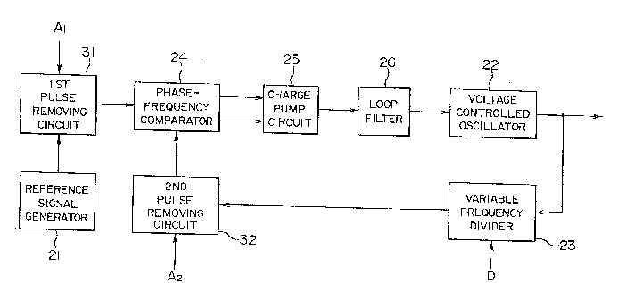
Referring to Fig. 2, the description will
proceed to a PLL frequency synthesizer according to a
25 first embodiment of this invention. The PLL frequency
synthesizer is similar in structure and operation to the
conventional PLL frequency synthesizer illustrated in
Fig. 1 except that the PLL frequency synthesizer further
comprises first and second pulse removing circuits 31 and
32 .
The first pulse removing circuit 31 is
connected between the reference signal generator 21 and
S the phase-frequency comparator 24. The second pulse
removing circuit 32 is connected between the variable
frequency divider 23 and the phase-frequency comparator
24 .
The first pulse removing circuit 31 is supplied
10 with the reference signal from the reference signal
generator 21 and first removing data Al indicative of a
first pulse number. Responsive to the first removing
data Al, the first pulse removing circuit 31 removes
pulses from the reference signal that are equal in number
15 to the first pulse number for a first predetermined cycle
to produce a first pulse removed signal. Instead of the
reference signal, the first pulse removed signal is
supplied to the phase-frequency comparator 24.
The second pulse removing circuit 32 is
20 supplied with the divided signal from the variable
frequency divider 23 and second removing data A2
indicative of a second pulse number. The second pulse
removing circuit 32 removes pulses from the divided
signal that are equal in number to the second pulse
25 number for a second predet~rm; n~d cycle to produce a
second pulse removed signal. Instead of the divided
signal, the second pulse removed signal is supplied to
the phase-frequency comparator 24.
4~
Therefore, the phase-frequency comparator 24
detects a phase-frequency difference between the first
and the second pulse removed signals to produce a
phase-frequency difference signal indic~tive of the
phase-frequency difference.
Turning to Fig. 3, the first pulse removing
circuit 31 comprises a first inverter 311, a first
counter 312, and a first AND gate 313. The first
inverter 311 is supplied with the reference signal from
the reference signal generator 21 (~ig. 2~ as a first
input pulse signal. The first inverter 311 inverts the
f irst input pulse signal to produce a f irst inverted
pulse signal. The first inverter 311 is connected to the
first counter 312 which is supplied with the first pulse
removing data. The first counter 312 counts up a first
count in synchronism with the first inverted pulse
signal. The first counter 312 produces a first time-up
signal when the first count increases up to the first
pulse number. The first time-up signal is supplied to
the first AND gate 313 which is supplied with the first
input pulse signal. Responsive to the first input pulse
signal and the first time-up signal~ the first AND gate
313 produces a first AND'ed signal as the first pulse
removed signal.
Similarly, the second pulse removing circuit 32
comprises a second inverter 321, a second counter 322,
and a second AND gate 323. The second inverter 321 is
supplied with the divided signal from the variable
2~2~6~
11
fre~uency divider 23 (Fig. 2) as a second input pulse
signal. The second inverter 321 inverts the second input
pulse signal to produce a second inverted pulse signal.
The second inverter 321 is connected to the second
5 counter 322 which is supplied with the second pulse
removing data. The second counter 322 counts up a second
count in synchronism with the second inverted pulse
signal. The second counter 322 produces a second time-up
signal when the second count increases up to the second
10 pulse number. The second time-up signal is supplied to
the second AND gate 323 which is supplied with the second
input pulse signal. 3~esponsive to the second input pulse
signal and the second time-up signal, 'che second AND gate
323 produces a second AND ' ed signal as the second pulse
15 removed signal.
Turning to Figs. 4(a) through (e), description
will be made as regards operation of the first pulse
removing circuit 31. The first input pulse signal is
depicted along Fig. 4(a). The first input pulse signal
20 is inverted by the first inverter 311 into the first
inverted pulse signal as shown in Fig. 4(b). The first
inverter 311 has an inverting delay time denoted to dl.
It will be assumed that the first counter 312
is supplied with the first pulse removing data indicative
25 of the first pulse number equal to four. In this event,
the first counter 312 counts up the first count at a
leading edge of each pulse in the first inverted pulse
signal. The first counter 312 produces the flrst time-up
~12~6~3
12
signal of ~ logical "1" level when the first count
increases up to the first pulse number, namely, four, as
shown in Fig. 4(c). The first counter 312 is reset to
produce the first time-up signal of a logical "0" level
S in response to another leading edge of the next
succeeding pulse of the f irst inverted pulse signal . The
first counter 312 has a counting delay time denoted to
d2 . Under the circumstances, the f irst AND gate 313
produces the first AND'ed signal as the first pulse
10 removed signal as shown in Fig. 4(d). That is, the first
AND gate 313 produces the first pulse removed signal
having pulses which is one-fifth as large as those of the
first input pulse signal. In other words, the first
pulse removing circuit 31 removes four pulses from the
15 reference signal for the first predetermined cycle which
has five pulses. The first AND gate 313 has a gate delay
time denoted to d3.
If the first pulse removing data indicates the
first pulse number equal to zero, the first counter 312
20 continuously produces the first time-up signal with the
logical "1" level. In this event, the first AND gate 313
produces the first pulse removed signal to which the
first input pulse signal is delayed for the gate delay
time t3 by the first AND gate 313 as shown in Fig. 4(e).
Operation of the second pulse removing circuit
32 is similar to that of the f irst pulse removing circuit
31 and the description thereof is therefore omitted.
Referring to Fig. S, the description will
, . . ~
~2~1~43
13
proceed to a PLL frequency synthesizer according to a
second: '-Q~ -nt of this invention. The PLL frequency
synthesizer is similar in structure and operation to the
conventional PLL frequency synthesizer illustrated in
Fig. 1 except that the PLL frequency synthesizer further
comprises a current controlling circuit 35.
The current controlling circuit 35 is connected
to the charge pump circuit 25 and is supplied with a
current command C. Responsive to the current command C,
the current controlling circuit 35 controls the current
for the charge pump circuit 25. More specifically, the
current command C is present while the output ~requency
is changed. The current controlling circuit 35 controls
the current so as to increase the current when the
current command C is present and then to gradually
decrease the current af ter the current command C becomes
absent. A little more in detail, the current controlling
circuit 35 comprises a charge-up control circuit and a
discharge control circuit.
Turning to Fig. 6, the charge pump circuit 25
comprises a complementary-symmetry metal-oxide-
semiconductor field-effect transistor (CMOSFET) which
consists of a p-channel MOSFET 36 and an n-channel MOSFET
37. Each of the MOSFETs 36 and 3~ has a gate ~P~min~l, a
drain ~P~;n~l, and a source ~Prm; n~l. The p-channel and
the n-channel MOSFETs 36 and 37 are ~oined at their drain
t~rm;n.qls which are connected to the loop filter 26 (Fig.
5~. The p-channel MOSFET 36 has the source t~rm;n;~ll
_ _ _ _ _ _ _ _ , . . . _ . .. . ...
~~fi~'~
14
which is connected to the charge-up control circuit of
the current controlling circuit 35. The n-channel MOSFET
37 has the source t~rm; nAl which is connected to the
discharge control circuit of the current controlling
5 circuit 3 5 . Both of the p-channel and the n-channel
MOSFETs 36 and 37 have the gate t~rmi nAl C which are
connected to the phase-frequency comparator 24 (Fig. 5).
More particularly, the phase-frequency difference signal
comprises lag and lead phase signals which indicate the
10 lag and the lead phases, respectively. The lag phase
signal is supplied to the gate terminal of the p-channel
MOSFET 36. The lead phase signal is supplied to the gate
,rmin~l of the n-channel MOSFET 37.
Supplied with the lag phase signal, the
15 p-channel MOSFET 36 is put into an ON state, thereby the
current flows from the charge-up control circuit to the
loop filter 26 through the p-channel MOSFET 36. Supplied
with the lead phase signal, the n-channel MOSFET 37 is
put into an ON state, thereby the current flows from the
20 loop filter 26 to the discharge control circuit through
the n-channel MOSFET 37.
Turning to Fig. 7, the charge-up control
circuit of the current controlling circuit 36 comprises a
switching element 41, an operational amplifier 42, an
25 n-channel MOSFET 43, first and second p-channel MOSFETs
44 and 45, first through third resistors 46, 47, and g8,
and a capacitor 49. The operational amplifier 42 has an
inverting input t~rminAl, a noninverting input t~rminAl,
21 22643
and an amplifier output t~rm; nAl .
The switching element 41 has a control input
terminal supplied with the current command C. The
switching element 41 is supplied with a positive source
5 voltage +VDD. The switchin~ element 41 is connected to
the noninverting input ~rm;nAl of the operational
amplifier 42. When the current command C is present or
has a logic one value, the switching element 41 turns on,
thereby the positive source voltage +VDD is supplied to
10 the noninverting input terminal of the operational
amplifier 42. The inverting input terminal of the
operational amplifier 42 is an end of the first resistor
46 which has another end grounded. The noninverting
input terminal of the operational amplifier 42 is
15 connected to an end of the second resistor 47 which has
another end grounded. The second resistor 47 is
connected to the capacitor 49 in parallel. The
noninverting input terminal of the operational amplifier
42 is also connected to an end of the third resistor 47
20 which has another end supplied with the positive source
voltage ~VDD. The amplifier output t~rminAl of the
operational amplif ier 42 is connected to the gate
tPrm;nAl of the n-channel MOSFET 43 which has the source
t~rm;nAl connected to the inverting input tf~rm;nAl of the
25 operational amplifier 42.
The n-channel ~qOSFET 43 has the drain tf~rm;nAl
which is connected to the drain t~rm;nAl of the first
p-channel ~OSFET 44. The drain t~-rm;n~l of the n-channel
_ _ _ _
43
16
MOSFET 43 is also connected to the g21te tlorm;n~lc of the
first and the second p-channel MOSFETs 44 and 45. Both
of the first ~nd the second p-channel MOSFETs 44 and 45
have the source terminals which are supplied with the
5 positive source voltage +VDD. The second p-channel
MOSFET 45 has the drain terminal which is connected to
the source terminal of the p-channel MOSFET 36 (Fig. 6).
Therefore, ~ combination of the first and the second
p-channel MOSFETs 44 and 45 composes a current Miller
lû circuit. The second p-channel MOSFET 45 has a gate width
which is N times as large as that of the first p-channel
MOSFET 44, where N represents a predetermined number.
When a first drain current Dl flows through the n-channel
MOSFET 43, through the second p-channel MOSFET 45 flows a
15 second drain current D2 which is N times as large as the
f irst drain current Dl .
Turning to Figs. 8(a) through (c), description
will be made as regards operation of the charge-up
control circuit of the current controlling circuit 36
20 illustrated in Fig. 7. It will be assumed that the first
through the third resistors 46 to 48 have first through
third resistance values, respectively, which are denoted
to R46, R47, and R48. The third resistance value R48 is
larger than the second resistance value R47. Figs. 8(a)
25 through (c) show the current command C, and the first and
the second drain currents Dl and D2 ~ respectively .
When the current command C is present or
becomes the logic one value at a time instant to ~ the
~ 2~3
17
switching element 41 turns on. Therefore, the capacitor
49 is charged up to a voltage of VDD. Through the
n-channel MOSFET 43 flows the first drain current Dl
which has a current value of VDD/R46. Therefore, through
5 the second p-channel MOSFET 45 flows the second drain
current D2 which has a current value of N x VDD/R46.
When the current command C becomes absent or
the logic zero value at a time instant t1, the switching
element 41 turns off. Therefore, the capacitor 49 is
10 exponentially discharged up to a voltage of R47/(R47 +
R48~ ) x VDD. As a result, the first drain current D
exponentially decreases up to ~ current value of
( 47/( 47 48) ) DD/ 46 cco ngly, the second
drain current D2 exponentially decreases up to a current
value of N x (R47/(R47 + R4g) ) x VDD/R46
The discharge control circuit of the current
controlling circuit 35 is similar in structure and
operation to the charge-up control circuit illustrated in
Fig. 7 except that the n-channel MOSFET 43 is replaced
20 with a p-channel MOSFET, the p-channel MOSFETs 44 and 45
are replaced with n-channel MOSFETs, and the positive
source voltage +VDD and the ground are exchanged each
other .
Referring to Fig. 9, the description will
25 proceed to a PLL frequency synthesizer according to a
third embodiment of this invention. The PLL frequency
gynthesizer i5 similar in ::~LLU~,~Ul~:: and operation to the
conventional PLL frequency synthesizer illustrated in
_ ., . .. _ _ . , .. . ... , , _ _ _ _ _ _ _ _ _ _ _ _ _ _ _ _ _ _
2~2~3
18
Flg. 1 except that the charge pump circuit is modified
from that illustrated in Fig. 1 as will later ~ecome
clear. The charge pump circuit is therefore depicted at
25a .
The illustrated charge pump circuit 25a
comprises a control circuit 51, a constant current
circuit 52, an integrating circuit 53, and a sample and
hold circuit 54.
The control circuit 51 is connected to the
phase-frequency comparator 24. Responsive to the
phase-frequency difference slgnal, the control circuit 51
produces first through third control signals. The first
through the third control signals are supplied to the
constant current circuit 52, the integrating circuit 53,
and the sample and hold circuit 54, respectively.
Responsive to the first control signal, the
constant current circuit 52 produces a constant current.
The constant current is supplied to the integrating
circuit 53. The integrating circuit 53 has an initial
voltage. The integrating circuit 53 integrates the
constant current to an integrated voltage. The
integrating circuit 53 is reset from the integrated
voltage to the initial voltage in response to the second
control signal. The integrated voltage is supplied to
2 5 the sample and hold circuit 54 . Responsive to the third
control signal, the sample and hold circuit 44 samples
the integrated voltage to hold a sampled voltage as a
held signal. The sample and hold circuit 44 supplies the
~12264~
19
held signal to the loop filter 26 as the current flow
control signal.
Referring to Fig. 10 in addition to Fig. 9,
description will be made as regards operation of the
S charge pump circuit 25~. In Fig. 10, the lag phase
signal, the constant current, the integrated voltage, and
the held signal are depicted along first through fourth
lines .
As shown in the first line in Fig. lO, the lag
lO phase signal is supplied from the phase-frequency
comparator 24 to the control circuit Sl during a first
time duration between a first time instant tl and a
second time instant t2 Under the circumstances, the
control circuit 51 produces the first control signal
lS during a second time duration between the first time
instant tl and a third time instant t3. Responsive to
the first control signal, the constant current circuit 52
produces the constant current during the second time
duration as shown in the second line in Fig. lO.
20 Therefore, the integrating circuit 53 integrates the
constant current to the integrated voltage during the
second time duration as shown in the third line in Fig.
10. After the third time instant t3, the integrating
circuit 53 keeps the integrated voltage. At a fourth
2 S time instant t4, the control circuit 51 produces the
third control signal. Responsive to the third control
signal, the sample and hold circuit 44 samples the
integrated voltage to hold a sampled voltage as a held
212~3
ZO,
signal at a fifth time instant t5. The held signal is
supplied to the loop filter 26 as the current flow
control signal . At a sixth time instant t6 ~ the control
circuit 51 produces the second control signal.
S T~cr.5ncive to the second control signal, the integrating
circuit 53 is reset from the integrated voltage to the
initial voltage. Therefore, the charge pump circuit 25a
increases a level of the current flow control signal in
response to the lag phase signal. In the similar
10 operation, the charge pump circuit 25a decreases the
level of the current flow control signal in response to
the lead phase signal.
It is understood that it is possible to set a
desired value to ~ gain of the charge pump circuit 25a by
lS changing the ratio of the first time duration to the
second time duration.
Referring to Fig. 11, the description will
proceed to a PLL frequency synthesizer according to a
fourth f~mhor~; -nt of this invention. The PLL frequency
20 synthesizer is similar in structure and operation to the
conventional PLL frequency synthesizer illustrated in
Fig. 1 except that the PLL frequency synthesizer further
comprises a control circuit 60.
The control circuit 60 is connected between the
25 phase-frequency comparator 24 and the charge pump circuit
25. The control circuit 60 is supplied with a control
enable signsl CE . R-~cr~-nci ve to the control enable
signal CE, the control circuit 60 acts as a modifying
~12~43
21
arrangement for modifying the phase-frequency difference
signal into a modified signal. Instead of the
phase-frequency difference signal, the modified signal is
supplied to the charge pump circuit 25. Therefore, the
5 charge pump circuit 25 controls, in response to the
modified signal, flow-in and flow-out of the current
supplied therefrom/to to produce the current flow control
signal. A little more in detail, the control circuit 60
is operable in one of a f irst mode and a second mode . At
lO first, the first mode will be described. The second mode
will be described later in the following.
In the ~irst mode, the control enable signal CE
is present while the output frequency is changed. The
phase-frequency difference signal comprises a pulse
15 sequence having pulses for a predetermined cycle that ~re
equal in number to a controllable number. When the
control enable signal CE is present, the control circuit
60 gradually decreases the controllable number until at
last a predet~rmin~fl final number. The predet-rm;ned
20 final number is, for example, one sixty-fourths as large
as the controllable number before being decreased.
Fig. 12 shows transient responses of the output
frequency in the conventional PLL frequency synthesizer
(Fig. l) and the PLL frequency synthesizer according to
25 the fourth embodiment. In Fig. 12, a transient response
for the conventional PLL frequency synthesizer is
depicted at a solid line. Another transient response for
the PLL frequency synthesizer according to the fourth
2~
22
~mho~; r-~t is depicted at a dotted line . As apparent
from Fig. 12, it is possible to raise up the tran3ient
response by decreasing the controllable number.
In the second mode, the control enable signal
CE is present in a steady state of the PLL frequency
synthesizer. The phase-frequency difference signal
comprises a pulse sequence having pulses each of which
has a controllable pulse width. The control circuit 60
narrows the controllable pulse width when the control
enable signal CE is present. It is possible to improve
unstableness in the PLL frequency synthesizer.
Referring to Fig. 13, the description will
proceed to a PLL ~requency synthesizer according to a
fifth embodiment of this invention. The PLL fre~uency
synthesizer is similar in structure and operation to the
conventional PLL frequency synthesizer except that the
PLL frequency synthesizer further comprises a switch 65,
a reset circuit 66, a control circuit 70, and a
digital-analog converter 71.
The control circuit 70 is supplied with the
designated dividing number D, the divided signal, the
phase-frequency difference signal. On changing the
output frequency, the control circuit 70 produces first
and second control signals. The control circuit 70 also
produces voltage data on changing the output frequency.
The voltage data represents a control voltage which is
defined by the designated dividing number D on the basis
of the phase-frequency difference signal. The control
_ _ _ _ _, . _ . , .. _ . .. , ... . .. , _ _ _ _
23 2 ~ 22643
circuit 70 determines the voltage data by carrying out
binary search on the phase-frequency difference signal.
The switch 65 is inserted between the loop
filter 26 and the voltage controlled oscillator 22. The
5 switch 65 is suppiied with the first control signal. The
switch 65 switches off in response to the first control
s ignal .
The loop filter 26 comprises first and second
resistors 261 and 262 and a filter capacitor 263. The
10 first resistor 261 has one end connected to the charge
pump circuit 25 and has another end connected to the
switch 65 and to one end of the second resistor. The
second resistor 262 has another end connected to one end
of the filter capacitor 263 which has another end
15 grounded.
The digital-analog converter 71 is supplied
with the voltage data from the control circuit 70. The
digital-analog converter 71 is activated only when the
output frequency is changed. The digital-analog
20 converter 71 converts the voltage data into the control
voltage. ~he control voltage is supplied to the voltage
controlled oscillator 22 and the filter capacitor 263 of
the loop f ilter 26 .
Responsive to the second control signal, the
25 charge pump circuit 25 is unactivated or put into a high
impedance state.
The reset circuit 66 is inserted between the
reference signal generator 29 and the phase-frequency
~ 2~
24
comparator 24. On the basis of the divided signal, the
control circuit 70 controls the reset circuit 66 so as to
make the reset circuit 66 produce a reset signal which
has a phase equal to that of the divided signal. The
5 reset signal is supplied to the phase-frequency
comparator 24 instead of the reference signal.
In the PLL frequency synthesizer illustrated in
Fig. 13, the digital-analog converter 71 supplies the
control voltage to both of the voltage controlled
oscillator 22 and the filter capacitor 263 of the loop
filter 26. The digital-analog converter 71 may be
modified into first and second digital-analog converters
71 and 72 as shown in Fig. 14. Under the circumstances,
the first digital-analog converter 71 supplies the
15 control voltage to the voltage controlled oscillator 22.
The second digital-analog converter 72 supplies the
control voltage to the filter capacitor 263 of the loop
f ilter 2 6 .