Note : Les descriptions sont présentées dans la langue officielle dans laquelle elles ont été soumises.
W O g3~09649 PCT/US92/~9746
2123226
LA~P BRIGHTNESS COMTROL CIRCUIT
WIT~ AMBIENT LIG~T CONPENSATION
This application is a continuation-in-part of U.S. Patent Application
Serlal Number 07/410,480 filed Sept~mber 21, 1989.
Field of the Invent1gn
The present invention relates broadly to a circuit for controlling
the brightness of a ~amp to maintain a desired ambient light level in an
area, despite variations in the amount of light supplied by a source
eYternal to the circuit.
~ack~round o~ the Invention
recent years, the fluorescent lamp, ~hich requires les~ energy
tha~n the incandescent la~p to produce ~he same amount of light, has
enjoyed increa~ing popularity. In many modern offices, fluorescent lamps
are used to the complete exclusion of incandescent lamps. Other gas
discharge la~ps, such as:sodium-vapor lamps, have replaced incandesoent
lamp~ in outdoor lighting applications.
To ~aintai~ high energy efficie~cy, reliable operation, and long lamp
life,~ these: gas di~charge la~ps may be operated in conjunction with a
reson~ant in~erter ballas:t circuit, such a : the ballast sho~n in the
nvent~r's U. S.:Pate~t 4,933,605.
Electro~ic dim~ing control circuits, such a~ the circuit disclosed in
the inve~tor'~ cope~ding U.S. Patent Applica~ion Ser~l Nu~ber 07/410,480
filed Sep~ember 21, 1989, haYe been used ~ith resonant inverter ballAs~s
~o proYide effective low-vol~age co~trol of gas discharge lamp brightness.
In the preferred embodiment of: the dimming circuit disclosed in the
071410,480 applicatio~, the dim~Lng level is controlled by a lo~ voltage
input level produced~by in~egrating a varisble pulse ~idth output rom an
electronic dimming control circuit.
Such clectrQni dimming circuits are generally provided with an
operator-~djusted manual control for setting :the desired level of gas
discharge lamp luminosity. ~It is also known tG turn lamps on and of~ in
re~ponse to pho~ocell measurement of ambient light levels. In a co~mon
application of this tech~ique, a photocell may ~e used to turn on a
W O 93/OgS49 PC~/USg2/09746
2 1 2 3 2 2 6 ~ ~rv
parking lot lamp during periods of darkness (i.e. night) and to turn the
lamp off during periods when sufficient eYternal light sources (such as
sunlight~ are available, thus con~erving energy.
In an office settiRg, each work are~ must at all times be provided
with at least a minimum level of light. The minimum necessary light
level is determined based on the tasks performed in the area. Fluorescent
lamps are generally installed in size and number sufficient-to provide the
minimum required light level in an area unter the asYumption that no other
light sources w~ll be available. A dimming circuit may be provided to
adjust the light output o~ the lamps, permitting multiple uses of the area
:
and compe~sation for changes in external light.
At times, other light sources are also operating in the area so that
,~ :
the amount of light produced i8 more than is needed, and the operation of
the lamps at the same intensity used in the absence of other light sources
is a waste of energy. ~For eYample, during the day sunlight may enter
through windows and skylights. When these other light sources are
available, the preset brightness of the gas discharge lamps will not be
. ~
needed in its entirety sincu the eYternal light source provides some or
ll of~ the minimum needed li~ht in the area. It would be passibl~ to
conserve 1arge quantitiès of energy, possibly up to 30Z of the energy used
to light a typical office building, if the light output of gas discharge
la~p~s could be limited~at all tlmes to the minimum required level.
Additionally, ~i~n~the workplace, it is usually desirable to have a
constant level~of light on ~ork surfaces. Contin~slly changing light
levels~resuIt in~pe~riods~of glare~when too much light is provided and
period of lncreased~diffLcu}ty in resolving images when too little light
is~pro~ided. A ~orker's~eyes must adjust to xesolve images at a gi~en
light ~level.~ ~Thus,~cQntinual light level variations requires continuous
optic~compen8atl0n,~and~thi;s eyestrain over time can adversely affect
health and;productivit~
~, U.S. Patents 4,48Z,844 to Sch~eer et al., and 4,371~812 and 4,394,603
to ~idmayer, show systems for dimmlng a fluorescent lamp in response to
ambie~t light condl~tions.~U.S. Patent 4,464,606 to Kane discloses a
fluorescent lamp dimmer with an electronic inverter that is controlled in
re6poDse to signals from~a celling-mounted ambient light sensor. The
dimming control circui~ sho~n operstes using low voltages and pulse width
modulation of the power to the lamps, but does ~ot integrate pulse-width
modulated control si~nals to produce the dimming control signal that
co~trols the vidth of the~ lamp svitching control pulse5. As far as the
W O 93/09649 PCT~S92/09746
,~ ~ 3 ~ 2 ~ 2~ 2 2 ~
inventor is a~are, electronic dimming control circuits of the type
disclossd in the aore~entioned pending application have not bee~
equipped wi~h circuits for adjusting the lamp output to mi~imize energy
consumpt~on while main~ai~ing a constan~ light level in an area.
SummarY of the Invention
Therefore, it is a general object of the present invention to provlde
an energy saving control circuit for gas discha~ge lampsO
~ other broad object of the present invention to pro~ide a circuit
~hic~ maintains a constant desired light level in an area.
A further object of the present invention is to provide a control
circuit for one or more gas~ discharge lamps ~hich maintains a constant
light level in an area by measuring the ambient light and reducing the
output of the lamps by the amount of light contributed by external light
sources.
Another important ob~ect of the present inventio~ is to provide a lo~
voltage ambient lipht monitori~g circuit having lo~ power requirements
hich can be ~ged to control a plurality of el~otronic balla ts to dim
balla8ted lamps~in response to the ambient light level.
Other o~ject~ of the invention will become Rpparent upon revie~ of
the;specification, dra~i~gs, and claims.
Thsse objects~and others are;achieved by providlng a comps:ct, easily
s~talled au~iliary circuit~uhich operates ~ith a lo~voltage co~trol
circuit associated vith~an electronic dimming lamp ballast. The auxiliary
c~rcuit:mo:difies the output of the control circuit to reduce the
brightness~ of the lamps~when excess ambient light i8 a~ailable, and
increases~the br~ghtne6~ of the lamps as available ambient light is
reduc~d. ~The auxiliary circuit is located i~ a ~mall housi~g whlch mounts
in a knockout~ plug of a `fluorescent ceiling fi~ture. The au~iliary
::
cirouit includes a photocell ~ha~ obtains information on ambient light
levels thr~ugh an a~bient light gathering prism mounted in the ceiling
near the fixture, and~connected to the circuit housing by a flexible fiber
optic cable. A sialgle circuit according to the invention can be used to
; control multiple ballasts~
~ ::
, ~ ~
O 93/0964~ 3 2 2 6 4 _ PCT/US92/09746
Brief Descri~tion of the Dra~inQs
Figuxe 1 is a circuit dia8ram of 8 solid-state electronic ballast
circuit sho~ing a pu~se-~idth modulation dimming control ci~cuit connected
to control the ballast;
Figure 2 is a detailed circuit diagram of the pulse-width mod~lation
dimming control circuit shovn in Figure l;
Figure 3 is a block-schematic diagram of the ambient-light responsi~e
control circuit of the present invention;
igure 4 is a schematic~diagra~ of the ambient-light responsive
electronic control circuit shown~in Figure 3;
Figure 5 is a diagram showing installation of the system of the
present i~vention in conJunctioD ~i~h a fluorescent ceiling fi~ture; and
Fi~gure 6a is a frontal~viev of the light-gathering prism of the
present invention, ~hile~Figure ~6b is a corresponding side viev of the
ame prism. ~ ~
Detailed ~escri~tion~of~the Preferred Embodiments
The~'lamp~ballast and~dimming circuit -i h which the present invention
may~be used ill first~be described ith reference to Figures 1 and 2.
Referring first;to~Figure 1, a resona~t :inverter solid-state dimming
bàllast~circult;is sho~n generally at 2. While a brief'description of the
co~n~truction~ and operation~of~this circuit; will be provided here, the
soiid~stat'e~dimming~ballast~2 is described;~completely in the inventor's
U.S.~patents~ 4,~993,605~and~4,~B64,482, the disclosure6 of which are
incorporated here *~by~reference.
;As~ ho~n~in~igure;l,; the~solid-state dim~ing ballast 2 comprises
pulse~idt~;modulator 4~, po-er ~s~itche6 6~a~d~8, resonant inductor 10,
reso~ant capacitor 12,~blocking capacitor 14, voltage diYider resistor 16,
v&riable re6istor 18, oscillator resistor 20, oscillator capacitor 22, and
oad~26.~ ~Load 26 is~provid~d with four terminals 38~ 39, 40 and 41. The
load 26 may ~pre~ferably be~ a~' fluorescent~ tube and ~ill frequently be
described as such herein.
The ~pulse width~modulator 4 may be a~conventional integrated circuit
such~as~a Motorola SG-2525, used ith~the~follo-ing termi~al connections:
Vcc (pin 15) is connected to a DC voltage sosrce 24, ~hile the Ground
termi~al (pin 12) is~connected to ground. The RT terminal (pin 6) is
: :
~ connected throug'h 0~6cillator resistor~20 to ground, and the CT terminal
W O 93/0964g PCT/US~2io9746
- 5 - 2 1 2 3 ~2 ~
(pin S) is connected through the oscillator capacitor 22 to ground. Vref
~pi~ 16) is connected to one terminal of ~oltage divider resi~tor 16. The
other texminal of voltage diYider resistor 16 is connected to the
Noninverting Input 17 (pin 2) of pulse width modulator 4 and also
connected to ground through variable resistor 18. Output A ~pin ll) and
Output B (pin 14) of pulse width modulator 4 are connec~ed respectively to
control terminals 33 and 29 of power svitches 8 and 6 respectively. For
reasons ~hich will ~-ecome clear upon description of further circuits
useful with the circuit of Figure I, the two terminals of variable
resistor 18 are preferably connected to terminals accessible from the
outside of any housi~g enclosing ballast 2 so that external circuits can
be connected to the~e terminals.
The po~er switches ~6 `and 8 may be of any suitable solid-state or
mechanical construction. Power svitch 6 is provided with two switching
terminals 28 and 30, ~nd power switch 8 likewise has two switching
terminals 32 and 34. Each of the power switches 6 and 8 are also provided
with control terminal 29 and 33 BS ~escribed previously. I~ response to
~;
a signa~ pulse on the control terminal '9 produced by the pulse ~idth
odulator 4, the pover switch 6 vill inte ~ally connect poYer terminals 28
and 30 ~o that devices~connected to~power terminal 28 ~ill be electrically
connected~with devices~connected to power termLnal 30. The power s~itch 8
1ike~ise connects power termina1s 32 and 34 in response to a signal pulse
fro-~the~pu1se vidth~modulator 4 transmitted tO the control terminal 33 of
power~switch 8~
A~ pos~itive~DC source; 36~is~connected to power terminal 28 of power
switch;~6~, and~pover terminal 30 is connected both tD the pover terminal 32
f power s~itch 8 and~to~one terminal of resonant inductor lO. The other
terminal of~resonant~ inductor ~lO is connected to terminal 38 of load 26.
Po~er term ~al 34 of po~er switch 8 is connected both to ground and to one
termlna~l;of~the blocking capacitor 14. The other termina1 of blocking
capacitor 14 i8 connected to terminal 40 of fluorescent tube (load) 26,
the terminal 40~being~at th~ opposite end of the tube from ~erminal 38
The`resonsnt capacitor~12 is~c~onnected across terminals 39 and 41 of the
fluorescent tube 26. m
OsciIlator resistor~20 and oscillator c~pacitor 22 together control
the ~requenc~ o~ the internal oscillator of pulse width modulator 4, ~hich
in turn controls the frequency of the output pulses from Outputs A and B
(pins tl and 14) of the pulse width modulator 4, which in turn control the
switchi~g of po~er to the fluorescent tube 26 as will be explained later
21~322~i
WO 93/09649 ~CI`/US92/09746
in more detail. Thus, the values of oscillator resistor 20 and oscillator
capacitor 22 are chosen to provide the desired frequency of po~er
ching at fluorescent tube 26.
The po~er switches 6 and 8 are alternately actuated by the signals Bt
control terminals 29 and 33 respectively. In operation, po~er s~itch 6 is
actuated first, so that DC current flows from DC source 36 through
resonant inductor 10, load 26, and resonant ~apacito~ 12, charging
blocking capacitor 14. Power switch 6 is then deactuated. After a brief
period of ti~e, po~er witch 8 is actuated, so that stored charge flows
from blocking capacitor 14 through load 26, resonant capacitor 12, and
resonant inductor 10 to ground, thus discharging blocking capacitor 14.
After a brief time delay this cycle is repeated, with the repetition at a
constsnt frequency determined by the values of oscillator resistor 20 and
oscillator~ capaci~or 22 as explained previously. The repetition of this
switching operation produces aD alternating current flow through load 26.
When the load 26 is a fluorescent tube, this current flo~ will excite the
internal gases of the tube, caus~ng the tube to glo~.
The amount of time~bet~een repetitlons of the cycle just explained is
dete~mined by the duty cycIe of the control pulses~produced by pulse ~idth
odulator 4 and transmitted to control terminals 29 and 33. As the duty
cycle of the control pulses increases, the duty cycle of pover applied to
he lo~d 26 will increase, increasing the apparcnt brigh~ness of the
fluorescent tube 26. C onverBely~ as the duty cycle of the co~trol p~lses
decreases, the apparent brightness of the fluorescent tube 26 ~ill
decrease. Thus, the circuit can be used to produce a dimming fu~ction.
The~ duty oycle of~the control pulses ~produccd by pulse width
modulator 4 is varied by~varying the voltage applied to the non-inverting
input 17~ of pulse ~:idth~modul~tor 4.
Ths dimming control circuit used in the di~ming ballas~ circuit o~
Figures l and 2, comprising~ pulse generating circuit 42, will no~ be
described in detail.
As shown in Figure 1, pulse generating cirruit 42 is connected as a
control input to the resonant inverter solid-state ballast 2. The output
43 of dimming control circuit 42 is connected to opto-isolator 48. If no
isoIation is desixed, output 43 could also be directly connected to the
base of an ordinary transistor substituted for phototransistor 52 and
having the same emitter a~d collector connections as phototransistor 52.
Opto-isolator 48 comprises a light-emitting diode (LED) S0 and a
phototransis~or 52. LED S0 is connected between o~tput 43 and ground.
W 0 ~3/09649 2 1 2 3 2 2 6 PcT/us92to974~
-- 7 --
Phototransistor 52 has its collector connected to non-inverting input 17
and its emitter connected to ground. Phototransistor 52 turns on in
response to light emis~ions from LED 50, which operates in response to the
pulses fro~ output 43. Opto-isolator 48 thus electrically isolates the
ballast 2 from the pulse generating circuit 42. ~he ballast circuitry may
contain large voltageæ and current, and as will be seen, controls for the
pulse generating circuit 42 will be handled by human operators. Thérefore,
this electrical isolation provides a substantial safety benefit.
The collector of phototransistor 52 is connected to non-inverting
input 17 of pul~e width modulator 4, while the emitter of phototransistor
52 is connected to ground. An integrating capacitor 46 is connected
between the non-in~erting input 17 and ground. The pulse generating
circuit 42 preferably generates a variable duty cycle, square wave pulse
;train at a fixed frequency greater than 1 kHz.
The output puIses at ~output 43 control the charging of integrating
capacitor 46. ~hen pulse generating circuit 42 produces a pulse at output
43, t~he voltage applied to the base of transistor 44 turns on
phototransistor 52, allowing~current to flo~ from the collector to the
emitter of~ the transistor 44~. Because the collector of phototransistor 52
is connected to the capacitor 46 and the non-inverting i~put 17, and since
the~ emitter of phototrans~istor 52~ is connected to ground, a pulse from
pul:se generating circuit 42;effectively grounds the integrating capacitor
46~.~ tend~ing~to discharge~the capacitor 46. ~hen output 43 is not
producing a pulse,~ phototransistor 52 is turned off, and integrating
capacitor 46 te~ds to~charge to the~ level of the voltage drop across
variablè resistor~ 18 ~as~determined by the voltage divider comprising
resi~tor 16 and~ariable~resistor 1~. ~
T~e~voltage ~t~non-inverting input 17 ~aries with the duty cycle of
the pulses at output 43. Since the output 43 prcduces a serles of pulses
at high~frequency. ~he~pulses produce a periodic pull up and down of the
`~ DG level across integrating capacitor 46. Integrating capacitor 46
integrates over time he DC level shift produced by the pulsed output 43,
so tha~t for~a given pulse duty cycle, a continuous DC voltage appears at
~on-inverting input 17. The DC voltage at non invertîng input 17 will
:: :
vary with the duty cycle of the pulsed output 43 in the follo~ing manner.
As the duty c~cle ~ncreases, the capacitor 46 will be grounded for a
relatively greater portion o~ time, and the voltage at non-inver~ing input
,
17 ~ill be reduced. Con~ersely ? as the duty cycle of pulses at output 43
~ is reduced, the voltage at non-inverting input 17 ~ill be increased.
:~:
W O 93/Og649 PCT/USg2/09746
2123~2~ 8 - ,<~c~i
Because the ~oltage level at no~-inverting input 17 controls the
apparent brightness of load 26, those skilled in the art will immediately
appreciate that the light output of load 26 can be adjusted by ~arying the
duty cycle of the pulses at output 43. Thus, the dimming of the solid-
~tate ballast is controlled by varying the duty cycle of a low-voltage
pulsed input to ths control circuitry of the ballast.
The circuit and operat~on of the pulse generating circuit 42 will now
be described in det&il with reference to Figure 2. As sho~n in Figure 2,
the pulse generating circuit 42 comprises a power supply section 54, a
reset section 56, a delay section 58, ~n overcurrent section 60, a pulse
control section 62, a brightness control section 64, and a variable duty
c~cle ~requency source 65.
. ~
The ~ariable duty cycle frequency source 65 may preferahly be an
UC2843 integrated circuit~ manufactured by Motorola, although other
integrated circuits could be~used, or a circuit could be constructed to
perform the necessary functions. The operation of the frequency source 65
is descri~ed in detail~in Motorola publlcations ~hich will be familiar and
accessible to those ~skilled in;the art. Ho~ever, the fu~ctions of the
pi~s~used~in this circuit~are~described in Table 1 in sufficient detail to
permit those~s~illed~in the rt to understand the circuit and to practice
the invention disclosed.~
Pin Connections of UC2843 Frequency Source
PIN NAME~ DESCRIPTION ~ ~
C`ompensation Voltage~may be applied exte~nally to vary the duty
cycle~of~the pulses. ~ ~
2~ Inv.~Input ~ ~ Not Used (~connected to~ground).
3 ~urrent Sense Inhibits~pulse output if~:more than one volt is applied
e~tern-lly.
4~ ~OSC ~ Provides~sa-tooth~wave output ~ith frequency depending
on~external circuitry.
5 ~ ~Ground ~ Connected~to ground.
6~ ~ 0ùtput ~Produces~variable duty cycle pulse output ~ith
frequency depending on external circuitry coDnected to
OSC terminal and duty~cycle depending Qn voltage
applied to Compensation terminal.
7 Vcc Power supply (+12v DC).
8 Vref Reference voltage output t5.1 VDC).
TABLE~l
.
W093/09~g 9 2 1 2 3 2 2 li Pcr/lJs92/o9746
Referring again to Figure 2, the power ~upply section 54 comprises a
transformer S6, a full-wave bridge rectifier 68, a capacitor isolation
diode 70, and a smoothing capacitor 72. The pover supply section 54 is
preferably al~o provided with a conventional three-termi~al, 12 volt
voltage regulator 84 a~d a~ associated capacitor 86. The voltage
regulator 84 ha an input texminal 88, an output terminal 90, and a ground
termlnal 92.
Alternating current input from an AC source 74 is connected to the
prlmary coil of transformer 66. The turns ratio of transformer 66 is
seleeted ~ith reference to the voltage of AC source 74 so that 12 volts AC
produced on ~he seco~dary coil. Full-wave bridge rectifier 68 is a
conven io~al device. The rectifier 68 has t~o lnput terminals 75 and 78
a~d t~o output terminals 80 snd 82. The tvo terminals of the secondary
coil of transformer 66 are ronnected respectively to input terminals 75
and 78 of rectifier 68. Output terminal 80 of rectifier 68 is connected
to circuit and Earth ground, ~hile output terminal 82 is connected to the
anode of isolatio~ diode 70 and provides a rectified, 12 vclt DC output
hareto. The cathode of dioda~70 is con~ected to the input terminal 88 of
:regulator 84 and to the positive ter~inal of s~oothing capacitor 72. The
negative terminal of~smoothing capacitor 72 is connected to both circuit
ground a~d Earth grou~d.
Tha output termi~al 90 of regul-tor 84 is connected to Vcc (pin 7) of
varlabla duty cycl~ ~frequancy source 65, a~d ground terminal 92 is
co~ected to ground~. The :capacitor 86 is connected betueen the output
:
ter~i~al 92 ~f regulator 84 and ground. The voltage regulator 84
co~pensd~es for ~ rl-t~ions~ in the~ voltage of AC source 74, thus
tabilizing tha 12 volt~DC pover provided to ~he integrased circuits of
freqna~cg:~sourca:65. ~ st6ble voltage supply for frequency source 65 is
ece~ 8 ary to:-void: ~a:ri-tio~s in the pu18 e sig~al output 43 of ~he
frequency source:65.: :
: ~ Pr~ferably, the 12 volt DC regulated output at output terminal 90 of
~ regulator 84 wil~ be us~ed as the DC source 24 connected to Vcc of the- ~ ; pulse width modulator 4 (shown in Figure l). In this vay 9 the entire
circuit ma~ be controlled by a single po~er s~itch ~not: shown in the
: : drawings). This ~itch may be any conve~tional switch and may be
talled in ths pover supply circuitry in a number of ways which are
~; conventional and ~ill be immediately apparent to those skiiled in ~he ar~.
: The brightness c~o~trol section 64 comprises a variable resistox 94
and a voltage divider resistor 9S. The v~riable resistor 94 is connected
W 0 93/Og649 2 1 2 3 2 2 6 lo PCT/US92/09746
between the compensation pin (pin 1) of frequency sOuEce 65 and ground.
Preferably, for reasons which ~ill become more obvious, the two terminals
of variable resistor 94 will be connected to terminals on the outside of 8
housing contaîning electronic dimming circuit 42 and/or ballast 2 so that
uires from external devices can bejconnected to the terminals of variable
resistor 94. ~oltage divider resistor 96 is connected bet~een Vref (pin
8) of frequency source 65 and the compensation pin (pin 1) of freque~cy
source 65. Vref (pin 8j of frequency source 65 provides a constant S.l
~olt DC signal. Thus, the variable resistor 94'and resistor 96 form a
.- :
voltage di~ider so that, as the variable resistor' 94 is adjusted, the
~oltage applied to the compensation pin (pin 1) of frequency source 65
will vary. As explained in Table 1, the voltage on the c~ompensation pin
(pin 1) of frequency source 65 controls the duty cycle of the pulses
produced at output 43, ~with the duty cycle determining the brightness of
the load 26 as described previously.
The po~er supply s~itch previousl7 described may be integrated ~ith
the variable resistor 94 in~a;manner well known in the art.
The delay section ~58 comprises a PNP transistor 98, a resistor 100,
capacitor 102. and resistor 104. The emitter of transistor 98 is connected
to~the~eompensatiQn~terminal ~pin l) of;~frequency source 65, while the
collector of~trans`is~tor 98 is~connected to ground. The base of transistor
~,',c~ 98~is~;~conneoted~to one terminal of resistor 104, and the other terminal of
t~e~resis,tor 104 ~is;~c~onnected to the output terminal 82 of bridge
,`'réctifier 68. ~The posltive~terminal of;capacltor lQ2 is connected to the
bà,se~;of~transistor~98~ ;whil~e~ the negative~terminal of capacitor 102 is
conneSted~to;~ground. ~Resistor 100~ is connected between the base of
trans~i8tor~98~and~ground.~
s~will~be~seen.~the~delay~section S8, provides advantageous operatioh
becausé.~in~;operation,~tbe~del~y section 58 suppres~es~trans-ission of the
d~mming signal at output~43~ at po~er-up. With ~the dimming signal
` suppressed by dela~'section 58,~ the tube 26 ~shown in Figure 2) is started~ at full brightness.~Full-brightness starting is,essential for two reasons:
s , ~ First,~full-brlghtnes~s starting prolon~gs the life of the fluorescent
tubes~.~Second, fluorescent tubes ~may not start at all if power is not
provided for the full~duty cycle.
The operation of~delay~section;58 to suppress ~he dimming s~gnal at
output 43 ~ill no~ be~described in detail. ~hen no power is applied to
the circuit 42 from AC source 74, the transistor 98 ~ill conduct fully,
, " ~ ~
~ ; thus effecti~ely grounding the compensation terminal ~pin 1) of frequency
W 0 ~3/09649 ~ 2 ~ 2 3 ~ 2 6 PCT/U~92/09746
source 65. ~hen the compensation terminal is grounded in this manner, a
zero duty cycle at output 4~ is selected. As explained previously, the
brightness of the load 26 (shown in Figure 2) varies inversely with the
duty cycle of the pulsed output 43. A zero duty cycle of the pulsed output
43 corrssponds to full brightness at the load 26 (6hown in Figure 2~.
Therefore, ~hen the transistor 98 is fully conductive, the load ~6 will be
at ~aYimum brightness.
When power is applied to the circuit 42, the capacitor 102 will
charge according to a time constant determined by the values of resistors
100 and 104 and capacitor 102. As the capacit~r 102 charges, the
transistor 98 will be rendered less conductive, u~til the transistor 98
cèases to conduct. ~hen the trsnsistor 98 ceases to conduct, the delay
section 58 will have no~effect OD the voltage at the compensation pin (pin
1) of frequency source 6S:.~ The ~oltage at the compensation pin (pin 1
will then be controlled entirely by the brightness control section 64.
Thus,~when power is applied to the circuit 42 and the resonant
inverter 801id-state ballast 2 (shovn in Figure 1), the delay section 58
will initially inhibit;any~dimm~ng of the load 26 (as shown in Figure 1),
regardless of:the setting of variable resistor 94 (the brightness
control)~ The Ioad 26~:~wi11 nstart~ at full brightness. After a brief
period of time, the délay section::S8 will cease to inhibit dimming and the
load 26 ~ill dim to the: leve~l~se~lected by means of variable resistor 94.
The :fluore~scent: lamp 26 does: not come on at full brightness and then
sudden~ly~become dim;~the;~steadily increasing ~oltage across capacitor 102
:as:~ charg2s reduces~the:conductance of transistor 98 steadily o~er a
brief:~period:of time. ~ The;~voltage at the compensation pin (pin 1) of
frequency sou~rce 65 will therefore increase steadily fro~ zero to the
level determined by~the~setting~of variable~resistor 94. hs a result, the
fluorescent~lamp~26 wi11~comè on at full brightness, and then dim to the
pre8et level in a smooth~;~and pleasing ma~ner.
The length of the delay produced by delay section 58 can be adjusted
by changing the value~of~resistors 100 and 104 and capacitor 102 in
accordance;with well-known~time constant principles.
During a po~er failure,~fluorescent lamp 26 wil} be e~tinguished. If
the power failure is brief,~the capacitor 102 may retain its charge, so
that delay section 58 will not provide the desired full-brightness startup
and transition to the~ set dimming level as described. As eYplained
previously, the ~amp 2:6:may not star~ at a low-brightness setting, and
even~ if the lamp 26 does start, its life ~ill be shortened by a low-
W O 93J0g649 2 1 2 3 ~ 2 6 12 - PCT/USg2/09746
intensity startup. Reset section 56 operates to reset the delay section
58 during a po~er fa~lure, preparing delay section 58 to operate properly
vhe~ power is re~urned to the circuit.
Reset section 56 comprises a diode 106, resistor 108, PNP transistor
110, filter capacitor 1129 and voltage divider resistsrs 114 and 116. The
anode of diode 106 is connected to the base of delay section transistor
98,~and the cathode of diode l06 i~ connected to one terminal of resistor
108. The other terQinal of resistor 108 is connected to the emitter of
transistor 110. Resistor 108 preferably has a small value, in the range
of 5-7 Ohms. The collector of transistor 110 is connected to ground. The
positive terminal of filter capacitor 112 is connected to the base of
transistor 110, while the negative terminal of the capacitor 112 is
connected to ground. One terminal of resistor 114 is connected to the
output~terminal 82 of ful~-~ave bridge rectifier 68, while the other
terminal of the resistor 114 is connected to the base of transistor 110.
Resistor 116 is connected between the base of transistor 110 and ground.
.
Resistors 114 ~and 116 together form a voltage divider which
de~termines the voltage~at the base of trahsistor 110. The values of
resistors 114 and ll6 are chosen with reference to the values of resistors
100 and~104 so that transistor 110 does not conduct while ~C power source
74 is~pro~:ding~power~to the circuit;42. The value of cap~citor 112 is
chose~wlth~reference to;the values of resistors 114 and ll~ so that, if
power~is removed from the circui~t, capacitor 112 ~ill discharge through
resistor;116~in~about~1 millisecond.
If a;~failure of~power~from ~AC source 74 occurs, the reset section 56
op~erates~as ollows~ The~ voltage at the base of transistor 110 falls to
zero ~ vlthin one~ milli:se~cond as the capacitor 112 dischar~ges through
iesistor ll6.~;Bec~u6e;delar;~ection capacitor lQ2 is still char~ed, the
voltage at the e~itter~of transistor 110 i8 considerably greater than
sero~. ~ Therefore, transistor l10 begins to conduct, effectively shorting
:
and discharging the delay section capacitor 102. Thus, the reset section
6~quickly prepares the~delay~section 58 so that the fluorescent tube 26
may be restarted automatical~ly at full brightness as descri~ed previously.
It should be~noted that diode 70 is provided in the power supply
section 54 to isolate the reset section 56 from filter capacitor 72 so
that, during a po~er interruption, filter capacitor 72 will not discharge
:
through the reset section 56 and prevent proper operation of the reset
section 56.
~ ~ The pulse control section 62 determines the frequency of the pulsed
:'
W 0 93/09649 - 13 ~ 2 1 2 3 2 2 ~ PCT/USg2/0974~
output 43 and limit~ the ms~imum dut~ cycle of the output pulses. Pulse
control section 62 comprises NPN transistor 118, frequency set capacitor
120, ~requency se~ refiistor 122, resistor 124, vRriable resistor 126, and
resistor 128. T~e base of transistor llB is connected to the oscillator
terminal (pin 4) of frequency source 65. The collector of transistor 118
is connected to Vref (pin 8) of frequency source 65, and the emitter of
transistor 118 is connected to one of the t~o terminals of resi.stor 124.
The other ter~inal of resi~tor 124 is connected to one of the two
te~minals of ~ariable reslstor 126. The other termin~l voltage appLied to
the current sense ter~inal (pi~ 3) will be approximately 1.4 volts.
The frequency source 65 will inhibit generation of a pulse signal at
output 43 whenever the voltage applied to the current sense terminal (pin
3) is greater than about one volt. Therefore, the effect of applying a
high frequency ramp oignal to the current sense terminal (pin 3) is to
suppress pulse generation during a portion of each ramp cycle.
The ramp signal applied to the current sense terminal (pin 3) has a
; peak~voltage Vmax. As ~e~piained previously, due to the action of the
voltage divider compri~ing resistors l24, 126, and lZB, Vmas is a fraction
of the~peak voltage of the~ramp signal at the osc~llator terminal (pin 4)
of~frequency~source~65. ~ Again, Vmax is preferably about 1.4 volts. A
single~ramp cycle~takes~place~over a time period encompassing a first time
period~and a second time period. In the first time period, the voltage of
the~ramp~ signal~rises~from~0~.6;vol~s to one volt; during this period, the
frequency~source 65 is~not;inhibited from trans-itting a pulse at output
43.~ 0f course,~whether~or;not a pulse is transmitted by frequency source
65,~and;the~actual du~ration of any~pulse transmit~ed, are determined by
brightness~control section 64,; delay section 58, and reset section 56 in
the~mà~er~e~plained~previous~ly. Duri~g the second time period, the
voltagé~ of~ the~ramp~signal applied to the current sen e terminal (pin 3)
exceeds one volt, and the~frequency source 6s is inhibited from producing
any signal at output 43,.~ Thus, the application o the ramp signal to the
current sense terminal (pin 3)~ limits the maximum dutg cycle of the pulses
at the output 43. In the~preerred embodiment described, with vmBx ~ 1.4
YoltS~ and vith the output~ 43 inhibited ~hen voltages greater than l.0
~olts are applied to~the current sense terminal (pin 3) of frequency
source 65, the maYimum duty c~cle of pulses at output 43 is SOX.
Limiting the pulsed output 43 to 8 50~ duty cycle places an upper
limit on the amount of dimming of the load 26. This llmitBtion is
~ desirable because dimming the load 26 excessively may shorten lamp life
::
::
W O 93/09649 P~T/USg2/Og746
2 1~ 2 2~ - 14 _
and ~ill in some cases result in an unpleasant flickering effect when the
load 26 i5 a fluoresce~t tube. The masimum duty c~cle of the pulsed
output 43 can be adJusted u8~ng variable resistor 126, and may be set at a
value othe~ than S02 as dictated by the requirements of the consumer or
the design parameters of the ballast 2.
Overcurrent section 60 is a protective circuit that disables pulsed
output 43 if excessive current is dra~n from output 43. Overcurrent
Eection 60 comprises a resistor 134 and a diode 136. The anode of diode
136 is connected to an output reference 45 which may serve as the ground
reference for the sig~al at output 43. The cathode of diode 136 is
connected to the current sense terminal (pin 3~ of frequency source 65.
Resistor 134 is connected~between the anode of diode 136 snd ground.
iode 136 prevents transmission of the ramp signal at the current sense
terminal;(pin 3) to the output reference 45.
The output 43 of frequency source 65 is inhibited when more than one
volt is~applied to the current sense terminal (pin 3). The voltage drop
across diode~136 is approxim-tely 0.6 volts; therefore, output 43 ~ill be
inhibited if the voltage~at the anode of diode 136 is greater than 1.6
volts.;~ This condition~will occur ~hen the voltage drop across resistor
134~is greater than~1.6~volts. Preferably, resistor 134 may be a 4.7 O~m
resistor, SQ that when more ;than 0.34 ~mperes of current is drawn from
output 43, the voltage drop across resistor 134 ~ill be greater than 1.6
volts~and t~e~output 43~will be~disabled. Thus, the overcurrent section
-60 prevents damage~to the circuit of the present invention.
Of~ course, e~ach~ballast 2~connected to pulse generating circuit 42
ill draw current, so~that~there is ~a~practlcal limit to the~ number of
ballasts~;~2~that can;be controlled by a si~gle p~lse generating circuit 42.
The ~pulse generatin;g c~ircuit as~disclosed~ill drive approsi~ately 16
ball;asts without esceeding 0.34~mp curre~t dra~ from output 43. However,
if it~is desired to~control more than 16 ballasts 2 using one pulse
generating circuit 42, an NPN power transistor can be used to increase the
fanout capability of~the~circuit 42. The base of the po~er transistor may
be~connected to the output~43, while the collector of the po~er transistor
is connected to a DC power;~source such as that provided at Vcc (pin 7) of
frequency source 65. The pulse~signal output to the ballasts 2 is then
take~ Rt the emitter of~the~po~er transistor. Numerous techniques of
increasing fanout capacit~-o an output are kno~n in the art. and will not
be described furth~er~ here. Thus, it can be seen that the fanout
capability of the ci~rcuit 42 can be eYpanded to allow control of almost
W 0 93/09649 - 15 - 6 Pc~/us92/~97~6
any number of ballasts 2 using well-known techniques.
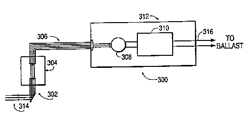
According to ~he present invention, the circuits shown in Figures 1
s~d 2 may also incorporate ~n ambient light responsive se~sing and control
circui~ 300, sho~n in block diagram form in Figure 3. Sensing and control
circuit 300 is a means for varying the brightness of load 26 in inverse
proportion to the amount of ambient light available rom other sources,
sueh as daylight. As ~hown in Figure 3, sensing and control circuit 300
comprises light converging prism 302, attachment housin~ 304, fiber optic
cable 306, ph~tocell 308, and processing circuit 310. Photocell 30~ and
processing circuit 310 are contained in housing 312.
The converging prism 302 is connected to an end of fiber optic cable
306 and ~is arranged to ga her Dmbient light 314 and direct the light 314
into one end of fiber optic cable 306. Fiber optic cable 306 carries the
àmbient light 314 from the end connected to converging prism 302 to its
other end, which is connected to housing 312 vith this other end in close
pro~imity to photocell 308. The light 314 passing through fiber optic
cable 306 impinges on photoce~ll 308:so that the output of photocell 308
~aries in response to the amount of light 314 gathered by prism 302, which
varies~ith the a~ou~t of ~ambient light available. Photocell 308 may be a
photoresistor which varles ~its~resistance in response to the amount of
light imp~nging upDn it~ so that its ~output~ is a pair of terminals
providi~g a varying resistance to a receiving circuit. For esample,
ph~tocell 308 may be a photoresistor such as part ~umber CL7PS~L made by
Claire~ Electro~ics Co. of Nount Vernon, New York. Thus, photocell 308
produces an output varying~vith the amount of ambient light available in
the:area~oovered by~the collection field of prism 302. Prism 302 can be
hsped~ as ~desired to colle~ct ambient light through a particular arc,
either narrow, widet or inte~rmediate in ~idth.
The output af~photocell 308 is con~ected to process mg circult 310.
Processing circuit: ~lO produces: a co~trol output compatible with th~
ballast 2 to control the brightness of the load 26 depending on the amount
of light available from other sources. If prism 3~2 is situated to sense
only light from source(s) other than load 26, processing circuit 310 ma~
be constructed to reduce the brightness of load 26 depending on the amount
of:light avail~able ~from the other source(s). Prism 302 ma~ also be
constructed and located so as to sense the total light in the area (from
.
~:: the load 26 and other sources). In particulart prism 302 may sense thetotal light reflecting from a critical work surface, such as ~ drafting
table or desk, where a constant light level is desired. In such cases,
W O 93J09649 PCT/US92/0~746
21232~6 - 16 ~
processing circuit 310 may be a feedback control circuit ~hich modifies
the brightness of load 26 in respo~se to changes in the amount of light
se~sed through photocell 308 to mainta~n a constant amount of light in the
area, and thu~ a constan~ output of photocell 308. Such a feedback
control circuit may incorporate proportional, integral, or derivati~e
algorithms, or a combination of t~o or more of these algorithms or other
algorithms commonly used in feedback control circuits. The output of
processing r~rcuit 310 is connected to the ballast 2 by control line~ 316
uhlch carry signals to effect control of the brightness functions o
ballast 2.
F:igure 4 is a schematic circuit diagram showing a preferred
embodl~ent of processing circuit 310. It is possible to construct a
feedback control circuit in accordance with the discussion above to
pro~ide an amou~t of light in an area that is substantially constant,
varying less than lZ from nominal. ~owever, in most practical office
applications, such precise control is not necessary. ~uman eyes are
r~la~ively insensitive to slight variations in light level~, and adjust
re~dily to compensate for such variations. In addition, most ~ork areas
are ~ot used for critical: detail ~ork. It has been found through
experimen~ation that the total light in most work areas can deviate up to
lOX from::the~ baseline level~without bein8 objectionable. Therefore, to
i~imize cost, complesit~,:,and ~aintenance, the preferred embodiment
provides a: relatively 6imple control:circuit which dims a controlled lamp
in~response to an increase in externally provided light but does not
measure total light directly to provide a~closed-loop feedback control
,~
8~:9tem. ~ : ~
In tbis ~embodiment,~ processing circuit 310 comprises,transistor 406,
capacitor~ 40~:7 diode 410, capacitor 412, potentiometer 414, potentiometer
416, r~istor 418, ground terminal 419, a~d output te~minal 420.
Tra~si~cor 406 ~is ~i NPN transistor of the N3904 t~pe, snd diode 410 is of
the lN914B type. Capacitor 408 is 0.01 uF; capacitor 412 is 47 uF;
resistor 418 is 27 kiloOhms; and potentiometers 414 and 416 are 100
kiloOhm potentiometers. Output terminal 420 and ground terminal 419 of
processing circuit 310 together make up the control lines 316, and are
con~ected to the ballast~2 in a mAnner that ~ill be described later in
detail.
Photocell 308 is connected to the base of transistor 406. The
collector of transistor 406 is connected to output termi~al 420~ and the
emi~ter of transistor 406 is connected through potentiometer 416 to
W 0 93/09649 17 - 2 1 2 3 PCT/VS92/09746
ground. D~ode 410 is connected between the base of transistor 406 and
output terminal 420. Capacitor 412 is connected between the ba~e of
transistor 406 and ground. Capacitor 408 is connected bet~een output
terminal 420 and ground. Photocell 308 has two termiDal6. One termLnal
of photocell 308 is connected to the base of transistor 406, and the other
terminal of photocell 308 is co~nected through potentiometer 414 to output
terminal 420 and through resistor 418 to ground. ~hile power/output
term~nal 420 pro~ides ~the operating voltage necessary to operate
processlng circuit 310, processing circuit 310 can also change the voltage
at output term~nal 420 if the voltage applied is sensitive to the
resistance of processing clrcuit 310. Thus, po~er/output terminal 420 is
both a source of power for, and~an output of, processing circuit 310.
Depending on the intensity of the ambient light, photocell 308
changes its~ resistance, producing a higher resistance at low light levels
and a lo~er resistance at~ higher light levels. Resistor 418 and
potentiometer 414 together form a voltage divider, dividing the volsage
applied through output ter-inal 420 so as to set the voltage applied to
photocoll~308. This voltage divider determines the base-to-emitter turn-
on voltage of the transistor 406. The resistance of the photocell 308 to
the~applied~volt~age ~determines the current flo~ing into the base of
transi tor 406.~ ~hen~the base~current of transistor 406 increases due to
an~ increase l~ thè~ mbient~light level sensed~by photoeell 308, the
col~lec~tor-to-emitter~current~in~transistor ~406 is increased. The
;po~er/~output~terminal;~420~ ill generally be connected to the middle of a
voltage~divider~reslstor~net~ork havi:ng a voltsge source with limited
current ~supplying capacity~. As a~result, ~hen~tran5istor 406 turns on,
dèpe~ding;o~ the~flow~of;curreDt~to the ba~e~of transistor 40S, the output
of~the~oltage source~cQnnected~to po~erjoutput terminal 420 ~ill begin to
;collapse.~ Thus,~the~magnitude~of the volt-ge at~po~er/output terminal 4~0
~ill be reduced.
Potentiometer 416 can be used to 5et a ma~imum di~ming point~ i.e. to
adjust;the amount of~dimming produced by the~ proces~ing circuit 310.
Potentiometer~416 must be~adjusted so that the masimum dimmin~ level ~ill
not~result in turn-off of the load 26. The choice of the capacitance of
capacitor 412 and the res~is ance of photocell 308 determines the delay or
response time or variati~on of the load brightness in response to
varistion in externally supplied light. Diode 410 operates to remove
charge from the capacitor 412 within about 47 milliseco~ds after the po~er
to ballast 2 is turned off, i.e. when ~Vref is removed. This operation
: ,
:;: :::
W O g3/09649 PCT/US92/09746
2123226
reset~ the circuit 310 to provide full lamp brightness ~pon reactivation
of ballast 2. Thus, diode 410 i8 a means for resetting the circuit to
ensure that the fluorescent lamp is al~ays stsrted at full intensit~ to
pro~ote reliable starti~g and longer lamp life.
Power/output terminal 420 will be connected to the circuits of Figure
1 and/or Figure 2, depending on the desired configuration and the nu~ber
of ballasts to be controlled by sensing and control circuit 300. It is a
particular advantage of the present invention that a single low-voltage,
lo~-power sensin~ and control circuit 300 can be used ~ithout substantial
modification to control one electronic ballast 2, or a l~rge number of
electronic bal~asts 2.
Re~erring to Figure 1, if the ambient light sensing device of the
presefit invention is to be used with a single ballast 2, and particularly
when the ballast 2 doe~ not have a dimming control circuit 42,
po-er/output terminal 420 will be connected to non-inverting input 17 (pin
2 of pulse width modulator 4), and the ground terminal 419 ~ill be
connected to the ground of Figure 1, i.e. to the grounded side of variable
resis~or 18 so that control lines 315 are connected across variable
resistor 18. Thus, powerfoutput terminal 420 i8 connected in the Yoltage
; divider comprising resistor 16 and~variable resistor 18. The operation of
; processing cireuit 310 as described above ~ilI reduce the voltage at ~on-
invert~ng input 17 ~n respo~se to an increase in estennally-provided light
se~sed b~ photocell 3~8.
hen ballast 2;is provided with an electronic dimming circuit 42 as
detailed~in F~gure~2, ;the~powertoutput termLnal 420 ~ill be connected to
the compeDsation pîn (Pl)~of~frequency source 55 and the ground ~erminal
;419~ will~be~connected~to the~ground of the~circuit of Figure 2, i.e. to
the gr~ou~ded~ side of ~ariable resistor 94. Thus, control lines 316 of
ensing~and co~trol circuit 300 are connected across variable resistor 94.
~it~ ~his co~nection, the~pouer/output terminal 420 is connected to the
i center of the voltage divider comprising resistor 96 and variable resistor
: ` : : :
94. As noted previously~. the compensation pin (P13 of frequency source 65
controls the duty cycle of the pulse vidth~modulated output of electronic
dimming circuit 42 vhich controls the brightness of the load 26. Thus,
hen transistor 406 is turned on by ambient light i~pinging on photocell
.
308, the voltage on the compensation pin ~ill be reduced and the pulse
output of electronic dimming circuit 42 ~ill have a reduced dut~ cycle.
ID this vay, the circuit of the present invention produces further dLmming
of he load 26 in response to an increase in ambient light. It is a
w093~0964g 19 - 2 1 2 3 ~ 2 6 PCT/US92/0~46
particular advantage of this embodiment that the dimming produced in
respo~se to eny increase in ambient light occurs ~ith reference to the
dim~ing level set by the occupant of the area using variable reæistor 94.
Thus, any desired l$ght level can be produced, and the selected level will
be approsimately maintained in spite of fluctuations in e~ternally
available light such as sunlight.~
..
A particular advantage of sensing and control circuit 300 of the
present invention is that this circuit can be used readily with one or
; many lighting fistures. In addition, sensing and control circuit 300 is
useful both with fixtures; driven only by electronic ballasts 2, and also
ith fixtures which further incorporate a lo~-voltage, pulse-witth
odulated brightness conerol~circuit such a~ electronic dimming circuit
42.~
Electronic dimming circuit 4~ can be used to control a plurality of
ballasts 2; therefore, if desired, a single sensing and control circuit
300 may be connected to sn~electronic dim~ing circuit 42 to control a
plurality of~ballasts 2 to dim their loads 26 in response to an increase
in~a~bient lighe. ~AlternaeiYely, the conerol lines 316 could be connected
in parallel to a;~plurality~of electronic dimming circuits 42 (across
variable~resistor 94~in~e-cb~Qs~ described previously). If a large number
of~electronic dimming circuits 42 and/or ~allasts 2 are to be connected to
~single sensing~Rnd conerol~circuit 300, sensing and cantrol circuit 300
s~ould be provided wieh amplifying means.~such as a trensistor circuit, to
incre~se~ies fanoue capQciey~ For eYample, an NPN po~er transistor can be
used~eo~in~rease the f~anout capability~ of sensing and control circuit 300
by connecting its~base~eo~the~outpue, its collector to a DC power source
suc'h~as~that provided~at Vcc~(pin 7) of ~frequency source 65, and
connecting~its emltter~ to;~ehe eleceronlc dimming circuits 42 and/or
b-llase6 2~t~o be conerolled ;thereby.~ Various technlques ~of increasing
fanout capaciey of the~output are within the ability of those of ordinary
i s~ilI in ehe art~ and wlll not be described further here. Thus, it can be
sèen that the fanout~cQpablllty~can be eYpanded to alloY control of almost
any~number of ballssts~ 2 andlor electronic~dimming circuies 42 using well-
kno~n tec~niques. ~
The design of the~present invention therefore permits a single
senslng~ and control~clrcuie~300 eo~be connected directly to the non-
inverting inputs 17 of~Q plurality~of ballasts 2, or the terminals Pl of a
plurality of electronlc~dimming circuits 42, to control a large number of
lamps. The use of a single sensing and control ci~cuit 300 as described
~: :: :
W O 93JOg6~g PCTIUS92/09746
3 2 2 6 ~ ?S
herein is particularly desirable since this method reduees cost and
e~hances rel~ability. In addition, a single sensing and control circuit
300 will provide more uniform control of lights in a given area such as in
a ~ingle room. Because of ambisnt light variation ~ithin areas, and
; because of variations in calibration ~nd response betveen multiple sensing
~ and control circuits 300, lamps in the same area that are controlled by
.
different sensing and co~trol circui~s 300 may e~hibit variation in light
~ output. This continual variation ~Ay be annoying to persons working in
: the area. Thus, it is prefer`able to ~se a single sensing and control
circuit 300 to control all the lamps in a lighting zone.
~:: Sensing and control circuit 300 is a low~Yoltage, low-power circuit
: and connects only to the low-voltage, low power side of the integrated
circuits uced in ballast 2 and electronic dimming circuit 42. Thus, ~ire~
: connecting sensing;and control circuit 300 to the various electronic
dimming circuits 42 andlor ballasts 2 controlled by the sensing and
, ~
control circuit 300 need not conform in size or routing to the code
: require-ents that w~uld be applicable to wires needed to operate higher
po~er and ~oltage circuits~. :
F:igure:5 :detail:s a preferred arrangement and construction of the
components~shown in Figure 3. ~ This arrangement is particularly designed
:or uee with fluoresc~ent:~li&hts~ installed in~ a typical office building
gr~id and panel'~:ceilin&~syatem. ~As shovn, a fisture 501 co~prise~ the
load~ 1uorescent~tube)~:26:and dim~ing ballast 2, located in fixture
hou~s~i~n&~5~02. ~FiYture 5~01~ is suspended in ceiling grid 504. A
.s. ~ ;translucent~diffuse;r~506 covers the components ln fixture hou~ing 502.
'Geiling~panels:~:508::fill;the sections in:ceiling grid 504 ~hich do not
contai~a~fi~ture~hougin&~502.:~Ballast~2 is~co~nected to and drives load
26~ Fi~ture~SOl will~generaLly contain th Ne or four similarly coDnected
loads~:~Z6~,~ although~for~cla`rit~onl~ one load~26 i8 S~OW~ in Figure 5.
: Fi~ture hous:ing 502~ls con~entional in that it has one or more holes
510 ~itb removable knockout:~pl~gs. Such holes are generally provided in
fixtures to accept~:cable: clamps and thus facilitate electrical po~er
service~to fixture 501.
ousing 312 is preferably a small, round plastic housing ~ith a body
513 snd a threaded~portion~512 smaller t~a~ the body 513. Threaded
portion~512 is installed:through hole:510:of fi~ture housing 502. ~ousing
312 is~held in place by a:~locking nut 514:of the t~pe normally used ~ith
electrical cable clamps~ Prom the end of housing 312 oppos~ite threaded
~ . portion 512, a~ adjustment for potentiometer 416 pro~ects so that this
:: :
WO ~3JOg64g PCI`/US92/~9746
. _ 21 ~ 21 23 22 6
adjustment is accessible without remo~ing or disturbing housing 312.
Potentiometer 416 may be of the type ~hich is adjustable using a
screwdrl~er, a~d will then be installed 80 that the adjustment is
acceæsible from outside housing 312. Also, fiber optic cable receptor 516
is provided on housing 312. Receptor 516 is a hollow tube of brass or
other appropriate material, threaded on the outside, and having four slots
cut i~ its e~t, transverse to the threads, at 90 degree intervals about
it~ circumference. The very~end of receptor 516 has sn unthreaded portion
~hich is beveled on the outside surface so that the beveled surface forms
a portion of a cone with its apex beyond the beveled end of receptor 516.
The hollo~ port on of receptor 516 recei~es the end of fi~er optic cable
;306, which slides in and is held in close proximity to photocell 308,
~hich is located~in housing 312 (as shown in Figure 3). The threads on
receptor 516 receive brass loc~in~ nut 518, which, through tightening onto
the beveled end of receptor 516, slightly compresses receptor 516 toward
its central longitudinal a~is, thus tightenin~ the slotted portio~s
thereof~against fiber optlc~cable 306. Thus, receptor 516 iæ a means for
lockably connec~ng fiber optic cable 306 to the housing 312 in a fi~ed
manner~ 80 that }ight~passing through fiber optic cable 3~6 shines on
photocell 308. ~ ~
Fiber optic cable 306~is~preferably a stranded fiber optic cable with
a plastic~ insulating jacket~520. Fiber optic cable 306 preferably has a
total ~diemeter on~t~he o~rder of 0.125 inches, and ~ill be sized in
conjunction with receptor~;516,~locking nut 518, and the components of
housing~;304~`to permit~good mechanical -nd light transmission connections
therebetween.
Housing~3~4 compris~es :;~threaded tube 522, locking nut 524, flst
washers~S26 and~528,~nd~nuts~ 530 and 532. Threaded tube 522 ma~ he a
brass tube, generally~imilar to the previously described receptor 516.
The tube 522 is hollo~throughout, and is threaded o~ the entire outside
~urface and on st 1east part of the Lnside surface to rece~ve pri~sm 302.
,
The end o~ tube 522 pro~imate to the fiber~optic cable 306 is slotted and
beveled as previously de~scribed with reference to the fiber optic cable
end ~f receptor 516. Locki~g nut 524 is identical to lockLng ~ut 518 and,
like loc~ing nut 518, serves as a me~ns to hold fiber op~ic cable 306
stationary relative to the associated fiber optic receiving tube. Of
:: : : :,
course, other types of compression fittings, su~ch as plumbing fittings,
and various other types of clamping hardware~designs could also be used
vithin the spirit of the invention.
W O 93/Og649 PCT~US92/0~746
2123226 22 ~ t
Tube 522 is prefer~bly 1.75 inches long, although other lengths could
~e u~ed. ~hat i8 important is tha~ tube 522 be of suficient length to
pass through the thickniess of ceiling panel 508 or other structural me~ber
through ~hich installation i8 desired, leaving suifficient ~pace on the
ends of tube 522 for connection of the necessary fittings. Specifically,
vashers 526 and 528 and nuts 530 and 532 are tightened on the outside
threads of tube 522 to hold housing 304 in place with respect to-ceiling
panel 508. Washers 526 and 528 are preferably large plastic ~ashers
formed in a color to match snd thus visually blend into the ceiling panel~
508.
Prism 302 is threaded into one end of the tube 522, and fiber optic
oable 306 is inserted into the other end of tube 522 and clamped, using
locking nut 524, in llght transferring relationship with prism 302, e.g.
so that the end of fiber optic: cable 306 abuts prism 302. Fiber optic
cable 306 is prefera~ly of sufficient length to permit desired positioning
of housing 304 relati~e to:the source of ambient light 314, while not
gerlerating excessive cost or producing so much light loss due ~o its
length that operation of the~circuit is adversely affected. In prac~ice,
a length of about 22 i~ches has been found effective.
Figures 6a and 6b show t~e construction of prism 302 in greater
detail. Prism 302 has a body 601 in the shape of a partially cut-out
cy}inder. The ~on-cut-ou:t portion of body 601 defines a collec~ing
surface~602,~2nd :the cut-~ut portion defInes a beveled re~lecting portion
606~. ~Figure 6a is a frontal vie~ of prism 302 particularly showing the
eolleeting surface 602~of:prism 302. Flgure 6b is a corresponding side
vie~ of~the same pr:ism, showing the shaping o~ the beveled, reflecting
portion~606. To facilitate~light collectio~, beveled portion 606 ~as two
substa~tially:flat:reflecting:~surfaces 6~8 and 610 which tend to reflect
ght~approiching from~different angles upYard through threaded portion
604.: Preferably,: the angle~between collécting sur~ace ~02 and reflec~ing
surface 608 is about 30 degrees, ~nd the angle bet~een collecting surface
602 and reflecting surface 610 is about 60 degrees. When prism 3~2 is
installed very close to a ceiling, the ref}ecting surfaces 608 and 610
ill be especially effecti~e at gathering light reflected from the ceiling
itself and also at gatherLng light comLng directly through a window. This
precise light gathering;capability makes possible the use of the less
complex circuits and simple algorithms of the preferred embodiment. Prism
302 is preferably made from clear Lucite or other appropriate formable,
trsnslucent optical m&terial~
:~
: ::
W O 93fOg64g - 23 _ 2 1 2 ~ ~ 2 6 PCT/US92/097~6
Positioning of the reflecting prism 302 is important to ~ssure
maYimum energy savi~gs and proper perfor~ance of the circuit. In general,
the prism should be positioned with the collecting surface 602 facing the
window or other ambient light source. The top of the t~threaded par~ of
prism 302 should be installed as nearly flush vith the lo~er surf~ce of
ceiling panel 508 as possible.
Prism 302 could also be installed to collect light from a region
below the hou~ing 304, such as from a work surface. ~owever, such an
arrangement is less preerred becaufie mo~ement in the area and variations
in the reflectivity of surfaces will significantly affect the amount of
light collected by the simple prism 302, causing undesired lighting
efects. A more complex le~s, capable of gathering light from a wide area
so as to average ~he light readings from the area I is required or
do~nward monitoring to avoid abrupt shif~s in load brigh~ness due to
movement in the area or placement of papers on a desk. A s~stem using
down~ard light collection will generally produce more accurate cor.trol of
load brigh~ncss, but significantly increases the cost and complexity of
the system. Thus, the system design shown in Figure S is preferred over a
do~n~ar~-aimed light ollection system because it provides acceptsble
operation with m~nimum cost and compleYity.
: i
~;
:: : :
: