Note : Les descriptions sont présentées dans la langue officielle dans laquelle elles ont été soumises.
21 24520
METHOD AND APPARATUS FOR AUTOMATICALLY VERIFYINGFAULTS AND MONITORING CHIPS IN A CHIP DETECTION CIRCUIT
Speclflcatlon
Fleld of the Inventlon
The present lnventlon relates to methods and
apparatuses for monltorlng chlps ln chlp detectlon clrcults.
Background of the Inventlon
Hellcopters are equlpped wlth many sensors that
advlse the pllot of the condltlon of varlous onboard systems.
There are normally open sensors, whlch close the clrcult when
the sensor ls actlvated, and normally closed sensors, whlch
open the clrcult when actlvated. The sensors are connected to
lndlcators such as warnlng llghts on the pllot's lnstrument
panel. The sensor ls typlcally located remote from the
lndlcator. Therefore, the electrical connectlons typlcally
pass through several harnesses, ~unctlon boxes, termlnal
boards, etc.
An example of a normally open sensor ls a chlp
detector. A chlp detector ls used to monltor the health or
alr worthlness of a hellcopter's transmlsslon or gear box,
whlch ls a vltal plece of equlpment. The presence of a
slgnlflcant number of metal chlps ln the transmlsslon fluld
usually lndlcates mechanlcal problems wlth the transmlsslon.
The chlp detector ls partlally lmmersed ln the transmlsslon
fluld so as to be exposed to the metal chlps clrculatlng
lnslde of the fluld. The chlp detector ls provlded wlth a
magnet so as to attract and retaln the metal chlps. The
presence or absence of *
-- 1 --
64312-21g( S)
, ~ .
~1 2~ 520
metal chips captured by the chip detector is indicated
both visually and electrically. The electrical
indication is provided by a warning light on the
instrument panel. If metal chips accumulate during
flight, the warning light is illuminated and the pilot
can safely land the helicopter, before the rotors lock
up .
The visual indication is provided between flights by
a ground mechanic. The mechanic physically removes the
chip detector from the transmission, visually inspects
the collection area on the chip detector for metal chips,
and then reinstalls the chip detector into the
transmission. A visual inspection of the chip detector
is required after the helicopter is flown for a specified
number of hours. (In Canada, the chip detector is
required to be visually inspected every day.)
Several problems can and have arisen due to the
frequent removal and installation of chip detectors.
Because the chip detector is in contact with transmission
fluid, failure to properly reinstall the chip detector
could result in a loss of fluid during flight. In fact,
this very problem occurred in a helicopter flying over
the Gulf of Mexico. The loss of transmission fluid
during flight resulted in a forced landing of the
helicopter on the water. One of the flotation devices on
the helicopter failed, resulting in the helicopter
flipping over and sinking.
Thus, with the required frequent handling of the
chip detector component of the transmission, the
possibility for loss of life or aircraft due to human
error is significant. The electrical indication circuit
provides no clue as to improper installation of an open
circuit sensor such as a chip detector. What is needed
is a system for detecting the improper installation of a
chip detector.
- 2124~20
Another problem caused by frequent handling of the
chip detector is broken wires. Wires lead from the chip
detector to the warning light in the cockpit instrument
panel. These wires can be easily broken as the chip
detector is handled during the visual inspection process.
A broken wire results in the disablement of the electric
circuit. In the prior art, there is Berrier, et al.,
U.S. Patent No. 5,045,840, owned by the assignee of the
present invention. Berrier, et al. provides a continuity
sensor that can be installed across an open circuit
device such as a chip detector. Upon the application of
power to the circuit in the cockpit, the continuity
sensor temporarily closes the circuit to illuminate the
warning light. If the warning light illuminates, the
interconnections leading from the warning light to the
chip detector are in working order. However, if the
warning light fails to illuminate, then the chip detector
circuit is inoperable.
The Berrier, et al. continuity sensor has proven to
be a noteworthy and much needed device. Before the
Berrier, et al. continuity sensor, prior art electrical
sensing circuits with normally open sensors were
vulnerable to open circuit faults. With the Berrier
continuity sensor, such open circuit faults can be
identified and corrected.
It is desired to supplement the Berrier, et al.
continuity sensor to, as mentioned above, detect if a
chip detector has been improperly installed. In
addition, it is desired to provide a system to monitor
the continuity of wires leading to the chip detector on a
continuous basis. Furtherstill, it is desired to provide
a system to monitor the electrical status of the chip
detector or other open circuit sensor so as to detect
degradation of the contacts.
By virtue of its magnetic field, a chip detector
installed in a transmission attracts chips of all sizes.
212~520
Much of the metallic chips that are attracted to and
retained by the chip detector are referred to as fuzz by
the aircraft industry. This fuzz is produced by normal
wear of components and represents no danger to the
helicopter or aircraft. New transmissions and engines in
particular produce relatively large amounts of fuzz
during their break-in periods. This fuzz builds up in
the chip detector, causing a short across the contacts of
the chip detector. Thus, the fuzz is detected by the
chip detector in the same manner as are larger chips.
Ideally, the chip detector would only detect the
presence of large chips. These large chips indicate that
the piece of equipment that is being monitored has
internal components that are failing and therefore a
catastrophic failure of the equipment is possibly
imminent .
The problem then is how to distinguish between the
relatively harmless fuzz and the larger size chips, which
indicate a problem with the equipment being monitored.
One way is to pull the chip detector out of its hole and
visually inspect it to determine the size of the chips.
But, as discussed above, this causes more problems (in
the form of a broken wire or potential loss of
transmission fluid if the chip detector is incorrectly
reinstalled) than it solves. Also, visual inspections
are unwise during flight.
There is a real need for a device that allows a
pilot, during flight, to verify if the chip detector has
detected large chips or just nuisance fuzz. Too many
false alarms caused by nuisance fuzz degrades the
effectiveness of the chip detector system, as a pilot is
more likely to attribute a chip indication to just
another false alarm.
In the prior art, there is Tauber, U.S. Patent No.
4,070,660, which shows an electrical circuit that burns
off the fuzz. A capacitor is connected across the chip
2 1 2 1 ~ 2 0
detector contacts. When no chips are present in the chip
detector, the capacitor charges to a voltage. When a
chip enters the chip detector, the capacitor discharges
through the chip. The idea is that the energy provided
by the discharging capacitor will heat and burn away the
unwanted fuzz, while leaving the larger chips, which
require detection, in the chip detector. The use of
electrical current to burn away small sized chips relies
on the phenomenon of resistive heating. As current is
passed through the chip, the resistance in the chip
causes heating. It is hoped that the temperature
increases to the point of melting or burning the chip.
The problem of the Tauber fuzz burner is its
unreliability. This is due to the nature of the energy
provided by a discharging capacitor. A capacitor
discharges exponentially, with the peak discharge current
through the chip occurring at the beginning of the
discharge. Thus, the peak energy is delivered to the
chip at the beginning of the discharge. In practice,
this produces instantaneous power at the points of
contact between the chip and the chip detector, resulting
in welding the chip to the contacts. Thus, instead of
burning fuzz away from the contacts of a chip detector,
the Tauber device does just the opposite.
Furthermore, the contacts of the chip detector are
immersed in oil circulating through the transmission.
This immersion is necessary, as it exposes the contacts
to the chips. However, the oil acts as a heat sink
around the chips. This requires more energy to burn away
a particular chip than if the chip was simply surrounded
by air. The prior art capacitor circuit is often unable
to deliver sufficient energy to burn away fuzz immersed
in the oil.
- 21 24520
Summary of the Invention
It is an object of the present invention to provide
a method and apparatus that eliminates fuzz from a chip
detector in a reliable and controlled manner.
Another object of the present invention is to
provide a method and apparatus that automatically
acquires information on the sizes of chips in a chip
detector.
The present invention provides an apparatus for
eliminating chips from a chip detector. The apparatus
includes means for detecting when a chip is in a chip
detector and means for producing plural pulses responsive
to the detecting means. The plural pulses include first
and second pulses. The first pulse has a different
energy content than the second pulse. The means for
producing plural pulses has timing means for causing the
production of the first pulse first, followed by the
second pulse if the chip is still in the chip detector
after the first pulse.
In one aspect of the present invention, the
apparatus further includes means for determining the size
of the chip based upon the energy content of the pulses
that are produced. In still another aspect, there is a
means for recording the pulses that the chip was
subjected to. In still another aspect, the means for
producing plural pulses includes means for varying
durations of the pulses such that the first pulse has a
first duration and the second pulse has a second
duration.
The present invention also provides a method for
eliminating and monitoring the presence of chips in a
chip detector. The method detects when a chip is in the
chip detector. The chip is subjected to a first pulse of
energy and a determination is made if the chip has
suffered burning or displacement as a result of the first
pulse. If the chip has not suffered burning or
21 24520
,
displacement as a result of the first pulse, then the chip is
subjected to a second pulse of energy that has a different
amount of energy than the first pulse. A determination is
made if the chip has suffered burning or displacement as a
result of the second pulse. The approximate size of the chip
is determined from the amount of energy required to burn or
displace the chip.
According to another aspect, the present invention
provides a system for monitoring a piece of equipment,
comprising: a) a chip detector; b) a pulse generator connected
to said chip detector so as to burn fuzz from said chip
detector, said pulse generator producing a square wave pulse;
c) a timer connected to said pulse generator so as to control
the width of said pulse.
The present invention is able to determine the sizes
of chips that are collected by a chip detector. Knowing the
size of chips allows the determination of the overall air
worthiness or operational readiness of a piece of equipment
that is being monitored. If the equipment produces small
chips, or fuzz, within a tolerance determined by the
manufacturer, then the equipment can remain in service. The
present invention provides quantitative data on the size of
chips, thereby reducing the number of false alarms to the
pilot or maintenance personnel. Also, the present invention
burns away the fuzz, thereby cleaning the chip detector. If
the equipment produces large chips, a serious and potentially
dangerous situation, then the pilot is notified in real time
by a display on the instrument panel.
64312-219(S)
21 24520
-
The present invention is able to provide
quantitative information on the sizes of chips by subjecting a
chip to plural pulses over time, with each pulse having a
different energy content. Thus, the chip is subjected to a
first pulse having a first energy content. The energy content
of the first pulse is selected at a low value so as only to
burn fuzz or chips that are within normal operating tolerances
for the equipment that is being monitored. If the chip is
fuzz, then it may be burned or displaced by the first pulse.
If the chip survives the first pulse, then it is subjected to
a second pulse having a second energy content. The second
pulse typically has a greater energy content than the first
pulse. If the chip is burned or
a'"7~ C - 7a -
~ ~ 64312-219(S)
2 12~ 5 20
displaced by a particular pulse, then the size of the
chip can be determined from the amount of energy required
to burn or displace that chip. In the preferred
embodiment, the chip is subjected to pulses of ever
increasing energy.
Brief Description of the Drawings
Fig. 1 is an electrical schematic diagram showing
the system of the present invention, in accordance with a
preferred embodiment.
Fig. 2 is a side, partially cut away view, of a chip
detector as modified for use in the present invention.
Figs. 3A and 3B are an electrical schematic diagram,
showing the chip monitoring apparatus of the present
invention, in accordance with a preferred embodiment.
Fig. 4 is a block diagram showing the data recorder
of the present invention.
Figs. 5A and 5B are schematic diagrams respectively
showing chip placement on chip detector contacts before
and after burn and displacement of the chip.
Figs. 6-9 are waveforms of pulses used to burn away
chips of various sizes on a chip detector.
Description of the Preferred Embodiment
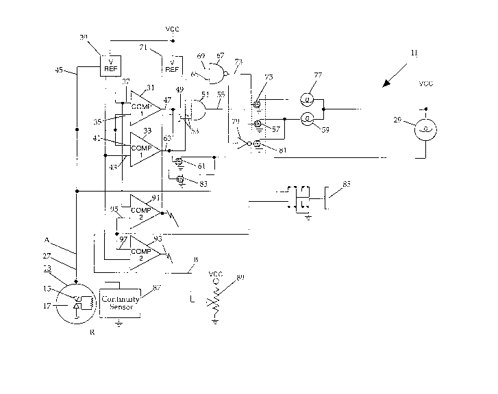
Referring the Fig. 1, the system 11 of the present
invention is shown. The system 11 monitors the status of
one or more sensors 13, 89 and also the status of the
respective sensor circuit. In the preferred embodiment,
the sensor is a chip detector 13, which is an open
circuited device. The chip detector 13 has been modified
by wiring a resistor R across the open circuit contacts
15, 17.
Referring to Fig. 2, the chip detector 13 is shown.
The chip detector has a removable plug 18 and a fixed or
seat portion 19. The seat 19 is fixed to the
transmission housing by threads. The plug 18 can be
212~52~
removed for visual inspection. The plug 18 has the tip
contact 15 while the seat has the ground contact 17. The
resistor R is located inside of the chip detector seat 19
so that when the chip detector plug 18 is inserted into
the seat in the transmission, the tip contact 15 of the
plug contacts one end of the resistor R. This tip
contact 15 is electrically connected to the terminal 21
on the plug, which receives a wire 27 (see Fig. 1). The
other end of the resistor R is connected to the ground
contact 17 of the seat, via a coil spring 23 in the seat.
This location of the resistor R allows chips to collect
in the area 25 between the tip contact 15 and the ground
contact 17.
Referring again to Fig. 1, the chip detector 13 is
connected via electronics to a warning light 29 located
inside of the instrument panel in the cockpit of a
helicopter. The warning light 29 is connected to a
supply voltage Vcc. When the electronics and/or the chip
detector complete the circuit to ground, the warning
light 29 illuminates.
The electronics provide comparators to detect a
voltage level above or below a predetermined level. Each
channel has a high comparator 31 and a low comparator 33.
Thus, for the chip detector channel, the high comparator
31 has one input 35 connected to the tip contact 15 of
the chip detector and the other input 37 connected to a
reference voltage supply 39. The reference voltage
supply 39 is connected to the supply voltage Vcc. The
reference voltage input 37 into the high comparator 31 is
set at a first predetermined level (e.g. 3-3.5 V). The
low comparator 33 has one input 41 connected to the tip
contact 15 of the chip detector and the other input 43
connected to the reference voltage supply 39. The
reference voltage input 43 into the low comparator is set
at a second predetermined level (e.g. O.7-1.5 V). The
reference voltage supply is also connected to the tip
212~520
contact through wire 45. This output on wire 45 of the
reference voltage supply 39 provides a high voltage to
the continuity sensor 87 (which will be explained below).
The high voltage is provided through a voltage divider,
which utilizes resistor R. Thus, if chips close the chip
detector circuit, the high voltage from wire 45 is pulled
low.
The output 47 of the high comparator 31 is connected
to one input 49 of an AND gate 51. The other inputs 53
of the AND gate 51 are connected to high comparator
outputs from the other channels which service other
sensors. The output 55 of the AND gate 51 is connected
to the gate of a field effect transistor (FET) 57. The
source and drain of the FET are connected to an amber
light 59 and ground respectively. The amber light 59 is
connected to the supply voltage Vcc. The output of the
high comparator 31 is also connected to the gate of a FET
61, which is connected in series to the instrument panel
warning light 29 for the chip detector.
The output 63 of the low comparator 33 is connected
to one input 65 of a NAND gate 67. The other input 69 of
the NAND gate 67 is connected to a reference voltage
supply 71, which supplies a third predetermined level
(e.g. 5 V) so as to produce a high input. The output 73
of the NAND gate 67 is connected to the gate of an FET 75
that drives a green light 77 by providing a connection to
ground. The green light 77 is connected to the supply
voltage Vcc. The output 73 of the NAND gate 67 is also
connected to the input of an inverter 79. The output of
the inverter 79 is connected to the gate of a FET 81 that
drives the amber light 59 by providing a connection to
ground. Thus, the amber light 59 is connected to two
FETS 57, 81 that are connected to ground in parallel with
each other. The output of the low comparator 33 is also
connected to a FET 83 that drives the instrument panel
warning light 29 by providing a connection to ground.
2124s2n
Thus, the lnstrument panel warnlng llght 29 ls connected to
two FETS 61, 83, that are respectlvely drlven by the hlgh and
low comparators. The two FETS 61, 83 are connected to ground
ln parallel with each other.
There is also provlded a press-to-test button 85 ln
the cockplt lnstrument panel. The press-to-test button 85 ls
normally open, but when pressed by a pllot, lt provldes a
connectlon to ground for the tlp contact lnputs 35, 41 of the
two comparators 31, 33. The green and amber llghts 77, 59 may
be physlcally located wlthln the press-to-test button 85 so as
to conserve lnstrument panel space.
There ls also provlded a contlnulty sensor 87
located ad~acent to the chlp detector 13. The contlnulty
sensor ls connected across the chlp detector contacts 15, 17.
The constructlon and operatlon of the contlnulty sensor 87 ls
descrlbed ln Berrler, et al., U.S. Patent No. 5,045,840. The
contlnulty sensor 87 provldes contlnulty across a chlp
detector whenever power ls applled to the wlre 27. Power ls
applled to the wlre 27 by the hlgh voltage on wlre 45,
whenever the system ll ls powered up. The contlnulty sensor
87 malntalns contlnulty for a predetermlned amount of tlme,
(e.g. 5-10 seconds~ and then breaks continulty.
The system 11 of the present lnventlon can servlce
plural channels, wlth each channel havlng a sensor. As
exempllfled ln Flg. 1, a flrst channel A ls connected to the
open clrcult chlp detector 13. A second channel B ls
connected to a sensor 89 that uses a potentlometer. The
second channel contalns lts own high and low comparators 91,
64312-219(S)
21 24520
93, a NAND gate (not shown) and two FETS ~not shown) for
drlving the respective lnstrument panel warning llght (not
shown). These electronlcs components of the second channel B
are identlcal ln conflguratlon to the electronlc components of
the flrst channel A. The
- lla -
64312-219(S)
212 1520
outputs of the comparators are connected to the same FETS
that drive the green and amber lights 77, 59. Thus, the
green and amber lights 77, 59 and their FET drivers 57,
75, 81 are common to all channel. In addition, the AND
gate 51 is common to all channels. The press-to-test
button 85 is also connected to the non-voltage reference
inputs 95, 97 of the comparators 91, 93.
With sensor 89, unlike the chip detector 13, a path
to ground through the potentiometer is already provided.
The reference voltages provided to the high and low
comparators 91, 93 can be the same as in the first
channel A, as shown in Fig. 1, or other reference
voltages can be provided.
The operation of the system will now be described in
general. An illuminated green light 77 indicates that
the fault monitoring system 11 is normal. If the sensor
is activated and changes voltage (as when the chip
detector is provided a path to ground through captured
chips), then the warning light 29 comes on and the green
light 77 stays on. This indicates that the system is
operating normally and that the sensor 13 has been
activated.
If an open circuit or high resistance fault is
present in channel A, the green light 77 goes off and the
amber light 59 and the respective warning light 29 come
on. The warning light allows the pilot to identify which
channel has the fault.
The system can be tested by either pressing the
press-to-test button 85 or applying power to the
continuity sensor 87. This illuminates all of the
lights; the green light 77, the amber light 59 and the
warning lights (such as 29) located in the instrument
panel. Illumination of all lights indicates that the
system is operating normally. If the green light fails
to come on during a test, then an open circuit or high
fault is present in one of the channels. Identification
212~520
of the channel occurs by ending the test (by releasing
the press-to-test button and by waiting for the
continuity sensor to turn off) so that the normal
channels turn off the respective warning lights. This
leaves the affected channel warning light 29 on.
If a fault is indicated by the amber and warning
lights, yet the system tests normally (all lights,
including the green light 77 come on), then this
indicates that there is a problem with the chip detector
13. The chip detector could be out of its hole (that is
the plug 18 is not in electrical contact with its seat
19) and transmission fluid may be leaking.
In general, the high comparator 31 is ground
seeking, changing state from low to high when a ground is
present in the channel. Such a ground can be caused due
to activation of the test button 85, the presence of
chips in the chip detector 13 or by a grounded wire. The
low comparator 33 is high seeking, changing state from
low to high when an open circuit or high resistance is
present in the channel. Such an open circuit or high
resistance can be caused by a broken or loose wire, the
chip detector being out of the hole (so that the tip
contact 15 no longer contacts the resistor R) or by the
chip detector contacts degrading due to corrosion or
coking (thereby causing a decrease in the leakage current
through resistor R). Resistor R is selected so as to
provide a suitable known leakage current. The resistor
R, in the preferred embodiment, is 12000 ohms. Specific
changes in the leakage current are detected by the two
comparators 31, 33.
Now, the operation of the system will be described
more specifically. The green light 77 is illuminated to
indicate that the system is normal. In a quiescent
state, the outputs of the high and low comparators 31, 33
are low. This drives the output of the NAND gate 67
high, which turns on FET 75 and illuminates the green
-- 2124~2~
light 77. Also, FET 81 is held open by the inverter, to
keep the amber light 59 off.
To test the system, the press-to-test button 85 is
pressed, wherein the green light stays on, and the amber
light 59 and the warning lights 29 illuminate. Closure
of the press-to-test button provides a ground to the
inputs 35, 41. The high comparator 31, which is ground
seeking, changes its output 47 to high. This high is
input to the AND gate 51. Assuming the other channels
are free of faults, all of the other channels also
provide high inputs into the AND gate. This causes the
AND gate 51 to switch high, which closes FET 57 to
illuminate the amber light 59. In addition, the high
output 47 of the high comparator 31 switches FET 61 on to
illuminate the warning light 29. In fact, all of the
warning lights for the other channels are illuminated.
Thus, when pressing the press-to-test button 85, all of
the lights are illuminated to indicate that the system is
in working order. When the press-to-test button is
released, the green light 77 stays on and the amber light
59 and the warning lights go off after the continuity
sensor 87 turns off.
The same test automatically occurs every time power
is first applied to the chip detector 13. Power is
applied to wire 27 by turning on the system, so as to
energize the reference voltage supply 39, or by releasing
the press-to-test button 85 after it has been pressed.
When power is applied, wire 27 has a high voltage, which
activates the continuity sensor 87. This application of
power causes the continuity sensor 87 to provide
continuity to ground for a predetermined amount of time
(for example 5 to 10 seconds). When continuity is
provided, the amber light 59 and the warning light 29
illuminate as when the press-to-test button is pressed.
Only those warning lights that are in a circuit with a
continuity sensor 87 are illuminated. After the
2 124~2~
predetermined amount of time has passed, the continuity
sensor opens and the amber light and warning light go
off.
If a sufficient amount of chips become lodged in the
chip detector 13, or if a wire is shorted to ground, then
the warning light 29 illuminates to inform the pilot of
an activation of the circuit. The chips in the chip
detector provide a path to ground. This ground causes
the output 47 of the high comparator 31 to go high. The
amber light 59 stays off because only one channel is
affected and the AND gate 51 stays low.
The operation of the system when a circuit fault is
present will now be described. If there is an open
circuit or high resistance in Channel A, the system 11
automatically detects this fault. The amber light 59 and
the warning light 29 are illuminated, while the green
light 77 is turned off. This indicates a fault condition
in the channel shown by the specific warning light 29.
The low comparator 33 senses the open circuit or high
resistance and switches its output 63 high. This
illuminates the warning light 29 and also the amber light
59 by way of the NAND gate 67 and the inverter 79. The
green light 77 is turned off. This condition will
persist until repaired.
When a fault is indicated, the system can be tested
by activating the press-to-test button 85. If the fault
is between the continuity sensor 87 and the comparators,
the green light 77 will stay off. This indicates a loose
or broken wire in the channel. However, if the green
light 77 comes on, this indicates that the circuit to the
continuity sensor 87 is operational, and that the chip
detector is presenting the fault condition. The chip
detector 13 is either out of the hole or the chip
detector has degraded due to contact corrosion or coking.
If the chip detector is out of the hole, the transmission
fluid could be leaking, a dangerous possibility.
- 212~520
Referring to Figs. 3A-9, the chip monitoring
apparatus will be described. The chip monitoring
apparatus, which is shown in Figs. 3A-4, is used to burn
away fuzz (or small chips) from the contacts of a chip
detector and to determine the approximate sizes of chips
based upon the amount of energy provided to chips. The
apparatus is designed to be used in conjunction with the
circuit of Fig. 1 and the chip detector of Fig. 2. The
chip monitoring apparatus records the information on the
sizes of the chips detected. Maintenance personnel or
pilots can utilize the information on chip size to
determine the air worthiness of the transmission or other
piece of equipment that is being monitored. This
information provides a history of the operation of the
transmission, giving an unprecedented and invaluable look
into the operational safety of the transmission.
Referring to Fig. 3A, the input 101 of the chip
monitoring apparatus is connected to the output of an OR
gate 103. The OR gate has plural inputs, each of which
is connected to the output of a high, or ground seeking,
comparator of the circuit of Fig. 1. For example, one
input is connected to the output 47 of the high
comparator 31 of Fig. 1. Other channels having chip
detectors or other open circuited devices are connected
to the other inputs of the OR gate 103.
The input 101 is connected to plural pulse
generators 105 tsee Figs. 3A and 3B). In the preferred
embodiment, there are four pulse generator 105A, 105B,
105C, 105D. Each pulse generator 105 has a timer 107 and
a one shot multivibrator 109. The timer 107 allows each
pulse generator to generate pulses in a coordinated
manner with respect to the pulse generators. In the
preferred embodiment, the timer 107 is an RC delay
network. The resistor 111 is connected in series with
the input 101 and the capacitor 113 is connected to
ground. The amount of delay is set by selecting the time
212452~
constant of the RC network 107. The output of the RC
network is connected to a noninverting input of a Schmitt
trigger 115 that is incorporated into the multivibrator
109. The multivibrator 109 has a resistor 117 and a
capacitor 119 connected to an input 121, which components
117, 119 control the width of the pulse that is produced
by the multivibrator. The output 123A, 123B, 123C, 123D
of each multivibrator is connected, through respective
resistors 125, to an input 127 of a summing amplifier
129, which sums the outputs from all of the pulse
generators. The output of the summing amplifier 129 is
connected to the gate of a power field effect transistor
(FET) 131. The source and drain of the FET 131 are
connected to a supply voltage VCC and to the chip
detector 13 via wire 27 (see Fig. 1). The comparators
31, 33, 91, 93 in Fig. 1 can be protected from the fuzz
burning pulse by diodes. Connected in series with the
supply voltage VCC is a current limiter 133, which is a
thermistor. The thermistor acts as a circuit breaker and
breaks the circuit if the current exceeds a predetermined
magnitude. Thus, the chip detector circuit is protected
against pulses that contain too much energy. The output
to the chip detector is protected with a diode 135.
The output 123A, 123B, 123C, 123D of each
multivibrator 109 is also connected to the input of a
respective buffer 137. The output of each buffer 137 is
connected to the input of a respective counter 139 (see
Fig. 4). The output of each counter 139 is connected to
the input of a data converter 141. The output of the
converter is connected to an input of a central
processing unit (CPU) 143. The CPU 143 is connected to
nonvolatile memory 145 in the form of an EPROM, and also
to an output interface 147, in the form of a data output
device. The output of the output interface 147 is
connected to a user interface 149 that is located in the
cockpit of a helicopter, in view of the pilot. The user
- 212i~2~
interface 149 includes a display to output data and a key
pad to input data. The CPU 143 has other inputs 151 as
well. These inputs are connected to the inputs of the OR
gate 103 in Fig. 3A. For example, one CPU input is
connected to the output 47 of the high comparator 31.
This allows the CPU to identify which channel or sensor
is being affected by chips.
The operation of the chip monitor will now be
described. When the chip detector 13 is installed into a
transmission, its contacts 15, 17 are exposed to oil
circulating in the transmission. Referring to Fig. 5A, a
magnet 18 is provided in the chip detector 13, between
the two contacts 15, 17. The magnet 18 attracts chips
that are circulating in the oil. When a chip 161 is
captured by the magnet, if it is large enough, it will
make contact with both contacts 15, 17, thereby shorting
across the contacts and completing the circuit. (If the
chip is not large enough to touch both contacts, then the
chip remains in place on the magnet, awaiting an
accumulation of more chips to short across the contacts
15, 17. )
Referring to Fig. 1, the connection-to-ground caused
by the chip is detected by the high comparator 31. The
output of the high comparator 31 changes to high. This
high output is routed through the OR gate 103 (see Fig.
3A) and thence to the input 101 to all of the pulse
generators 105A, 105B, 105C, 105D. When the input 101
goes high, the timers 107 begin to charge the capacitors.
The timer 107 of each pulse generator can be
programmed to provide the desired coordination between
the pulse generators. Programming occurs by selecting a
resistor 111 and a capacitor 113 to provide the desired
time constant. For example, in the preferred embodiment,
the timer 107 of pulse generator 105A provides a 500 ms
delay, the timer of pulse generator 105B provides a 1000
ms delay, the timer of pulse generator 105C provides a
18
212~15~0
1500 ms delay and the timer of pulse generator 105D
provides a 2000 ms delay. In addition to programming
when each pulse generator will be used, each pulse
generator can be programmed to provide pulses of selected
widths. Pulse widths are programmed by selecting the
resistor 117 and capacitor 119 to provide the desired
time constant to the multivibrator. For example, pulse
generator 105A provides a pulse of 35 ms duration, pulse
generator 105B provides a pulse of 70 ms, pulse generator
105C provides a pulse of 100 ms, and pulse generator 105D
provides a pulse of 150 ms duration.
When the input 101 goes high, the capacitors 113 in
the timers 107 begin charging. After 500 ms, the timer
of pulse generator 105A produces a high input to the
Schmitt trigger 115. This causes the multivibrator 109
of pulse generator 105A to produce a pulse on its output
123A. This pulse is routed through the summing amplifier
129 to the FET 131, causing the FET to conduct. Energy
from the power supply VCC is thus connected to the chip
detector 13. The current limiter maintains the energy
pulse in the preferred embodiment to 10 volts, 10 amps.
The first pulse is 35 ms in duration, after which the
output 123A of the multivibrator goes low, thereby
turning off the FET 131.
Thus, pulse generator 105A will provide the first
energy pulse to the chip. If the chip is still in place
across the contacts 15, 17 after being subjected to the
first pulse, then after 1000 ms from the detection of the
chip, the timer of pulse generator 105B will cause pulse
generator 105B to provide the second energy pulse to the
chip. The second energy pulse contains more energy than
the first energy pulse, because the second energy pulse
has a longer duration. If the chip is still in place
after being subjected to the second pulse, then, after a
delay of 1500 ms, pulse generator 105C will provide the
third energy pulse to the chip. If the chip is still in
2l~4s2a
place after being subjected to the third pulse, then,
after a delay of 2000 ms, pulse generator 105D will
provide the fourth energy pulse to the chip. In this
manner, the pulse generators are automatically
coordinated with each other in providing energy pulses to
the chip in a stepwise manner. The chip is subjected to
plural pulses of energy over time, with the energy
content of each pulse increasing over time. The pilot of
the aircraft is unaware of these activities until
notified that a large chip is present, as described
below.
Referring to Figs. 5A and 5B, the energy pulse is
routed through the chip 161. As current flows through
the chip, resistive heating causes the chip to diminish
and deform. In Fig. 5A, the chip 161 is shown before it
has been subjected to an energy pulse. Fig. 5B shows the
chip 161A after being subjected to an energy pulse. The
chip 161A has curled and been displaced away from contact
15. In most cases, the displacement of the chip 161A is
sufficient to place the chip back into circulation in the
oil system, where the chip is then removed by an oil
filter. Breaking electrical contact with the contact 15
removes the short across the chip detector. This causes
the output of the high comparator 31 in Fig. 1 to go low,
and thereby causes input 101 (Figs. 3A, 3B) to go low.
When input 101 is low, the capacitors 113 in the timers
107 begin to discharge, effectively disabling the pulse
generators. Thus, no more pulses are generated.
When the energy pulse (in the form of electrical
current) is routed through the chip 161, a magnetic field
is developed around the chip as a result of the current
flowing through the chip. This magnetic field is
oriented at 90 degrees with respect to the magnetic field
of the chip detector magnet 18. Thus, the energy pulse
not only heats and burns the chip, but produces a
magnetic field that is repulsed by the chip detector
2124~2~
-
magnet 18, further aiding the displacement of the chip
from the contacts 15, 17.
In the preferred embodiment, the energy pulses of
all of the pulse generators are square pulses of the same
voltage and amperage. This simplifies the determination
of the size of the chip, which will be explained in more
detail below.
The chip monitor can be connected to plural chip
detectors. The inputs to the chip eliminator have
already been described. The output to the FET 131 is
connected to all of the chip detectors. The particular
chip detector that has the shorting chip will draw the
energy pulse, because the other chip detectors will
present open circuits.
Every time a pulse generator produces a pulse, that
pulse is counted by the respective counter 139 (see Fig.
4). The CPU 143, which has a clock, records the pulses
produced by each pulse generator over time in its memory
145. In addition, the CPU records the number of and
duration of pulses provided to each chip detector. This
information is obtained by correlating the inputs 151 to
the inputs from the counters. Thus, the CPU records a
full history of each chip detector.
In addition, the CPU 143 provides an indication on
the user interface 149. A threshold for each channel can
be programmed into the CPU. The threshold can be a
predetermined pulse width. The CPU compares the pulses
from the specific pulse generators and the specific
channels to the particular threshold for a channel. If
the threshold has been met or exceeded, an indication is
given on the display in the user interface 149. For
example, if the threshold pulse width is 150 ms, and if
pulse generator 105D is utilized to produce a pulse,
then, the CPU 143 indicates that this threshold has been
met by providing an indication on the user interface.
This informs the pilot that a large chip was discovered
212~20
in the chip detector. The number and energy content of
the pulses is determined by the particular piece of
equipment being monitored. For example, the Allison
250-C20 turbine allows the elimination of chips up to
.032 square inches in cross-sectional area. Therefore,
the threshold would be set to provide an indication if a
chip larger than .032 square inches is detected. Another
threshold that can be programmed is a specified number of
pulses of a specified width within a specified duration.
If the CPU detects this threshold, then an indication is
given on the user interface. The indication can be a
number code, which specifically identifies the threshold
that has been met or exceeded in the channel on which it
has occurred. A user can also operate the user interface
to obtain access to the information stored by the CPU in
its memory.
The chip monitoring apparatus can determine the size
of chips. Referring to Figs. 6-9, there are shown
waveforms that illustrate the burning of chips. In the
Figs., a pulse of 70 ms duration was used and the chips
were immersed in transmission oil. In Fig. 6, the chip
was burned and displaced away from the chip detector
contacts in about 10 ms. During the burning, the voltage
increases thereby indicating that the resistance
increases as the chip heats up. After 10 ms, the voltage
increases to full voltage, indicating an open circuit and
the displacement of the chip from at least one contact of
the chip detector.
The cross-sectional area of the chip burned in Fig.
6 was about .021 square inches. The larger the
cross-sectional area of the chip, the more energy that is
required to burn and displace the chip. This is because
the chip has more mass that must be resistively heated.
In Fig. 6, the pulse begins at a base line of 0 V,
indicating a short across the chip detector contacts.
After the end of the pulse, the voltage across the chip
212452~
detector contacts, which are now open due to the burning
of the chip, returns to a reference level (3.7 V in the
preferred embodiment). This reference level is due to
the leakage resistance R (see Fig. 1) across the chip
detector contacts. In Fig. 7, the chip was burned and
displaced in about 25 ms. The cross-sectional area of
the chip in Fig. 7 was about .050 square inches. Fig. 7
also shows the occurrence of a secondary burn. This
secondary burn was caused by a secondary fragment. The
secondary fragment burn occurred in under 10 ms. In Fig.
8, the chip had a cross-sectional area of about .095
square inches. In the first 55 ms of the pulse, the chip
is burned and fragmented. One of the fragments returns,
almost instantaneously to the chip detector contacts,
causing a rise in voltage and another resistive heating.
By the end of the pulse, the chip fragment is still in
contact with the chip detector contacts. This causes the
CPU to initiate a warning on the user interface. In Fig.
9, the chip is too large to be burned by the pulse.
Therefore, Fig. 9 shows a short across the chip detector
contacts for the duration of the pulse.
A look up table is created and stored in the EPROM
145. The look up table, which is empirically created
from data such as that described above, is used to
determine the size of the chip being burned. For
example, if the chip survives a 35 ms pulse but does not
survive a 70 ms pulse, the apparatus determines that the
chip size is between 35 mils and 100 mils. If the chip
survives a 70 ms pulse, but not a 100 ms pulse, then the
apparatus determines that the chip size is between 100
mils and 700 mils. If the chip survives a 100 ms pulse
but not a 150 ms pulse, then the apparatus determines if
the chip survives a 100 ms pulse but not a 150 ms pulse,
then the apparatus determines if the chip size is between
700 mils and 1000 mils.
2124S20
Although the invention has been described as
providing plural pulses of different energies using a
pulse generator for each pulse width, energy pulses can
be generated with other arrangements. For example, pulse
generators can be ganged together and their pulses
temporally blended or amplitude blended. Also, the
resolution in determining chip size can be varied by
either increasing or decreasing the differences in energy
of the pulses. For example, if a higher resolution was
desired in determining chip size, the sequence of pulses
could increase by 25 ms. Thus, a first pulse would have
a first duration of 25 ms, followed by a second pulse
having a duration of 50 ms, followed by a third pulse
having a duration of 75 ms, and so on.
Although the drawings have shown the energy pulses
used to burn fuzz as being square pulses, other types of
energy shapes could be used. For example, a more rounded
pulse of energy could be used to burn away fuzz.
Although the present invention has been described
with reference to helicopters, it can be used in other
electrical systems as well.
The foregoing disclosure and the showings made in
the drawings are merely illustrative of the principles of
this invention and are not to be interpreted in a
limiting sense.
24