Note : Les descriptions sont présentées dans la langue officielle dans laquelle elles ont été soumises.
212~910
~ BACKGROUND OF THE INVENTION
The present lnventlon ls dlrected generally to
dlgltal apparatus, and more partlcularly, to apparatus that
lncorporates ln the scan chaln of a scannable clrcult the
state lnformatlon conveyed to a nonscannable unlt.
Today's state of the art ln dlgltal deslgn often
wlll requlre the lncorporatlon of features that wlll allow the
deslgn to be tested - both durlng productlon and when ln the
fleld ln the hands of the end user. One of the more popular
test technlques used ln dlgltal deslgns for test
lmplementatlon is what ls termed a "scan based deslgn". Thls
lnvolves addlng loglc to the deslgn of conventlonal dlgltal
clrcultry so that, ln response to test slgnals, the elemental
storage unlts (e.g., latches, reglster stages, fllp flops, and
the llke) of the dlgltal clrcultry can be conflgured lnto one
or more extended shlft reglsters ("scan chalns"). Test
patterns ("vectors") may then be lntroduced ("scanned") lnto
the scan chalns so formed, and the dlgltal clrcultry returned
to lts standard conflguratlon and allowed to run normally for
one or more of lts operatlng cycles. The scan chalns are then
reformed so that the resultant reglstered state of the digltal
system can be removed and examlned.
Alternatlvely, the dlgltal clrcult under test can be
allowed to run normally untll lt reaches a polnt in tlme when
the scan test halts normal operation of the circuit. The scan
chain configurations are then formed, and the registered state
of the circuitry ls removed, observed, relnstated, and the
unlt allowed to proceed after belng returned to lts standard
configuration. ~
64157-426
2124910
Scan deslgns provide an effective and efflclent
method of establlshlng controllablllty and observablllty over
the "reglstered state" of the dlgltal clrcultry (i.e., the
states assumed by the elemental memory unlts at any moment ln
tlme) ln that operatlon of the unlt or clrcult under test can
be stopped at any polnt ln tlme, the unlt reconflgured to lts
scan conflguration, and that state retrieved, observed, and
replaced. The circuit under test may then be returned to the
normal operating mode and continue untll lt ls agaln stopped
and lts reglstered state observed as descrlbed.
Often, deslgns of dlgltal unlts ln the current art
will combine such scannable components with standard, off-the-
shelf components (e.g., microprocessors, random access
memories (RAMs), and the llke) that are not deslgned to be
scannable. Thus, the registered state of these standard
components are, therefore, outside the controllable and
observable domalns of a scan test procedure. Thls comblnatlon
of scannable components wlth nonscannable components can
signlflcantly llmit the testablllty of the overall
comblnatlon.
Slnce such nonscannable parts cannot be lncluded ln
any scan strlng, any lnltlal reglstered state values they may
hold after a scan test (or an lnltlallzatlon) of a scannable
part must be consldered lndetermlnate. Thls lndeterminate
state will tend to propagate lndeterminism elsewhere, forclng
use of one of several remedies: (1) add extra logic to block
the formatlon and propagatlon of such lndetermlnate state (and
accept large untestable areas of clrcultry); (2) add
compllcated test sequences followlng the scan to functionally
-- 2
64157-426
2124910
ellminate the lndetermlnate state; or, (3) some comblnatlon of
the foregolng.
It can be seen, therefore, that a need exlsts for
the reglstered state of non-scannable clrcultry to co-exlst
wlth scannable clrcultry for testlng purposes.
SUMMARY OF THE INVENTION
The present lnvention recognlzes that certaln of the
reglstered state of a nonscannable component originates with,
and wlll be transferred from the scannable unit. According to
the present invention, therefore, the reglstered state
transferred by the scannable component ls repllcated and
stored in scannable registers contalned ln the scannable
clrcultry. Thus, scan testlng the scannable component wlll
also permlt observatlon of the defect-free reglstered state of
the nonscannable element.
More speclflcally, the invention provides apparatus
for including state information of a nonscannable dlgital
devlce ln a scan of a scannable devlce, the state lnformatlon
belng transferred from an output of the scannable devlce to
the nonscannable dlgltal devlce, the apparatus comprlslng:
scannable reglster means, formlng a part of the scannable
devlce and coupled ln parallel wlth the output of the
scannable devlce, for recelvlng the state lnformatlon
communlcated from the output to the nonscannable devlce, the
scannable reglster means belng conflgured to be lncluded ln
the scan of the scannable devlce; and means for momentarlly
communicating the reglster means to the nonscannable device at
the concluslon of the scan of the scannable devlce.
The lnventlon also provldes apparatus for lncludlng
-- 3
64157-426
2124910
state lnformatlon of a nonscannable dlgltal devlce ln a scan
of a scannable devlce, the scannable devlce selectlvely
operatlng ln a run mode, durlng whlch the state lnformatlon ls
transferred from an output of the scannable devlce to the non-
scannable dlgltal devlce, and a test mode durlng whlch data ls
scanned from the scannable devlce, the apparatus comprlslng:
a scannable reglster element coupled ln parallel wlth the
output of the scannable devlce to recelve and temporarlly
store the state lnformatlon communlcated from the output of
the scannable devlce to the nonscannable dlgltal devlce, the
scannable reglster element operatlng to lnclude the state
lnformatlon wlth the data durlng the test mode; and a clrcult
that momentarlly communlcates the scannable reglster element
to the nonscannable devlce at the concluslon of the test mode.
From another aspect the lnventlon provldes a method
of lncludlng state lnformatlon of a non-scannable logic unlt
ln a scan of a scannable loglc unlt havlng a plurallty of
elemental storage unlts, a flrst number of the elemental
storage unlts formlng a flrst data reglster when the scannable
loglc unlt ls ln an operatlng mode, the plurallty of elemental
storage unlts, lncludlng the flrst number of the elemental
storage unlts, formlng at least one extended shlft reglster ln
response to test slgnals that place the scannable loglc unlt
ln a test mode, and a nonscannable loglc unlt havlng a second
data reglster coupled to recelve data from the flrst data
reglster, the method lncludlng the steps of: formlng, from a
second number of the plurallty of the elemental storage unlts,
a thlrd data reglster when the scannable loglc unlt ls ln sald
operatlng mode, the thlrd data reglster belng coupled to recelve,
- 3a -
64157-426
2124910
in parallel, the data coupled to the second data reglster from
the flrst data reglster; and selectlvely communlcatlng data
from the first data reglster to the second data reglster when
the scannable loglc unlt ls ln the operatlng mode, and from
the thlrd data reglster to the second data reglster at the
concluslon of the test mode.
BRIEF DESCRIPTION OF THE DRAWINGS
Flg. 1 ls a dlagrammatlc lllustratlon of a scannable
component, lncorporatlng the lnventlon, coupled to a
nonscannable component;
- 3b -
.~
64157-426
212~910
Fig. 2 is a timing diagram illustrating operation of
the invention; and
Fig. 3 is a flow chart illustrating use of the
invention to switch between run modes of operation and scan
modes of operation.
DESCRIPTION OF THE PREFERRED EMBODIMENT
Referring now to the figures, and for the moment
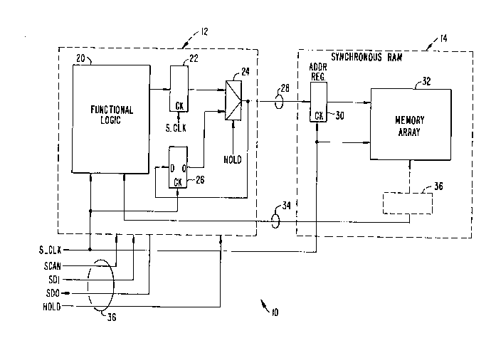
specifically Fig. 1, there is illustrated a portion of a
digital system, designated with the reference numeral 10, that
includes two system components 12 and 14. The component 12,
which may be an application specific integrated circuit
(ASIC), and the component 14 is a synchronous random access
memory (RAM). As Fig. 1 shows, the component 12 includes
functional logic 20 which symbolically represents most of the
digital circuitry of the component 12, coupled to an output
register 22. The content of the output register, via a
multiplexer 24, supplies multi-bit addresses to an address bus
28 which communicates the addresses to an address register 30
of the synchronous RAM 14. Data is accessed from a memory
array 32 of the synchronous RAM 14 in response to the
addresses received by the address register 30, and
communicated to the component 12 by the data bus 34.
The output of the multiplexer 24 is also coupled to
a shadow register 26 to receive the addresses communicated to
the address register 30.
The component 12 is designed to be scannable in the
sense discussed above, i.e., its elemental memory units (e.g.,
flip flops, registers, latches, and the like), including those
2124910
_ 5
that may make up the functional logic 20 and output and shadow
registers 22, 26, are configurable to operate in one of the
three modes of "run" (the element operates normally, and the
SCAN and HOLD signals are de-asserted), "hold" (the element
holds its state), and "scan" (all the elements configured to
form one or more scan chains). For this purpose the component
12 is coupled to a test bus 36 for receiving test signals SCAN
and HOLD from a test control device (not shown). In addition,
the test bus 36 includes a scan data in (SDI) line for
serially communicating test vectors (data strings) or to
replace the previously removed registered state of the
component 12. of course the component must be placed in the
scan mode by assertion of the SCAN test signal to receive data
on the SDI line.
The registered state of the component 12 is serially
removed, again when in scan mode, via the scan data out (SDO)
output line.
When operating normally (i.e., during run mode), the
HOLD test signal is not asserted. And, it is the non-asserted
state of HOLD that operates the multiplexer 24 to select and
pass the content of the output register 22 to the address bus
28, and to the shadow and address registers 26, 30 (all under
the synchronous control of the system clock, S_CLK). During
run mode, from time to time, addresses will be communicated to
the synchronous RAM 14 for addressing memory locations of the
memory array 32 from which data is to be accessed, or at which
data will be written. The addresses are received and
temporarily held in address register 30 of the synchronous RAM
14 to address the memory array 32. Thus, the synchronous RAM
2124910
_ 6
14 is an example of a commercial element having non-scannable
registered elements (unless designed to be scannable - which
in the context of this discussion it is not).
Referring now to Figs. 2 and 3, operation of the
S present invention to include the registered state (i.e., the
content of register 30) in the scan chain will now be
described. At some point in time during run mode (e.g., step
40 of Fig. 3) it is decided to enter scan mode for the purpose
of removing for examination the registered state of the system
10. How the decision is made is not important to the present
invention; it could be made programmatically (as by the test
unit (not shown) that supplies the test signals) or by a user
who may manually commands the test unit to replace the
registered state of the system 10.
Before continuing, consider for the moment Fig. 2
which illustrates the contents of the registers 22, 26, and
30. Prior to leaving the run mode (step 40, Fig. 3), at time
to~ the output register receives address A. At the next cycle
of the system clock, S_CLK, time tl, the output register
receives address B, and the prior content of the output
register 22 (address A) is transferred to the address register
30 and the shadow register 26. The next cycle (time t2) finds
address B in the shadow and address registers 26, 30, while
the output register 22 has received address C.
Now, prior to time t3, the decision is made to
remove the registered state of the system 10 (i.e., component
12) so that, at time t3, the run mode of step 40 (Fig. 3) is
departed in favor of step 42 in which the HOLD test signal is
asserted. The HOLD signal will, as explained above, freeze
212~911
_ 7
the registered state of the component 12 while asserted.
However, since the synchronous RAM 14 is non-scannable, the
HOLD signal will have no effect on it or its registered state
(i.e., address register 30). The SCAN signal would then be
asserted to reconfigure the scannable registers into one or
more scan chains, and the state of the component 12 serially
removed, using S_CLK, via the scan data out (SDO) signal line
where it can be observed.
Assertion of the SCAN signal will operate to block
the write enable to the synchronous RAM 14 to ensure that no
spurious write operations are performed during the scan of the
component 12.
The S_CLK signal, which is also applied to the
synchronous RAM 14, and during extraction of the state of the
component, the address register 30 of the synchronous RAM will
continually be clocked by S_CLK to receive whatever content
the output register 22 (which, of course, is part of the scan
chain) contains at the time. Thus, at the completion of the
scan it is not known what the content of the address register
30 will be, i.e., its content is indeterminant. When, after
observation, the removed state is returned to the component 12
(via the scan data in SDI signal line), and the component
returned to its normal, operating state, the content of the
indeterminate content of the address register 30 can be
propagated by the data that may be written to, or accessed
from the memory array 32 when operation is resumed. It is
this propagation of indeterminate state to which the invention
directed.
2124910
The problem of propagatlon of lndetermlnate states
as a result of scannlng the component 12 ls obvlated by
addltlon of the multlplexer 24 and the shadow reglster 26. As
wlll also be seen, use of the multlplexer 24 and shadow
reglster 26 provldes an effectlve technlque for lncludlng the
fault-free reglstered state (l.e., address reglster 30) of
what ls essentlally a nonscannable part ln the scan strlng of
the component 12.
Durlng normal operatlon the HOLD slgnal that is
applied to the control lnput of the multlplexer 24 ls not
asserted so that the content of the output reglster 22 ls
selected and passed by the multlplexer 24 to the address
reglster 30. However, each tlme the state (l.e., address) of
the output reglster 22 ls so transferred, lt ls also
communlcated to and stored ln the shadow reglster 26.
At tlme t3, the test control unlt responds to
programmatlc or user lnput to assert the HOLD test slgnal and
the run mode step 40 ls left vla step 42 ln favor of step 44
(Flg. 3). At tlme t4, wlth the HOLD slgnal asserted, the
output reglster 22 and shadow reglster 26 wlll dlsregard S_CLK
and retaln thelr content (l.e., addresses D and C,
respectlvely). However, address reglster 30 ls not affected
by the HOLD signal, and wlll therefore recelve the address C
applled to lt by reglster 26 (vla the MUX 24). The SCAN
slgnal ls asserted ln step 44 (Flg. 3) at tlme t4 and the HOLD
slgnal deasserted. Then, durlng step 46 (whlch wlll last many
S_CLK cycles), the state of the component 12 ls removed and
64157-426
_`~ 2124910
replaced, during which tlme the address reglster 30 becomes
lndetermlnate. As noted above, the SCAN slgnal wlll operate
to block write enable to
- 8a -
64157-426
2124910
g
the synchronous RAM 14. Thus, while SCAN is asserted, the
synchronous RAM 14 is prevented from performing write
operations, and the various indeterminate states assumed by
the component 12 during scan testing will not affect the
content of the memory array 32 of the synchronous RAM 14.
After the appropriate number (n-l) of S CLK pulses,
the scan is completed, and the state of the component 12
restored. That restoration will place the component 12 in the
state it had entered before leaving the run mode n favor of
being scanned, i.e, the state it held just before time t3.
Before the system 10 is returned to the run mode (step 40 -
Fig. 3), however the indeterminate state of the address
register 30 must be replaced; if not, this indeterminacy will
be propagated through the system (e.g., back into the
component 12) by data that will be read from (or written to) a
memory location of the memory array 32 that will have no
meaning in the ongoing scheme of operation.
In order to restore the address register 30 to a
proper state, the HOLD is asserted for one or more clock
periods of S CLK. During the clock period beginning at time
tn l, the address scanned into the shadow register will be
selected by the multiplexer 24 and placed on the address bus
28 by the HOLD signal, and loaded in the address register 30.
At time tn the system 10 is returned to the run mode (step 40 -
Fig. 3), by de-asserting the SCAN and HOLD signals, where
operation resumes from the point just before steps 42, 44 were
entered, and with the address register 30 containing the
proper address C. Note that when operation is resumed, the
content of the address regis~er 30 is no longer unknown, i.e,
212491~
-- 10
indeterminate but, rather, contains the quantity that it
should, address C. Note also that the information state that
would have been contained in the address register 30 when scan
test was initiated was, in fact, included in the scan test by
it being stored in the shadow register 26.
Thus, it should now be apparent to those skilled in
this art that the invention allows a scan of a scannable
device to be followed by normal operation without elaborate
procedures to remove any indeterminate states. In addition,
the invention is capable of including the defect-free state of
a nonscannable part (i.e., address register 30 of the
synchronous RAM 14) in the scan.
The invention has been described in the context of a
limited "pipeline" architecture that includes the output
register 26 and address register 30, permitting at least some
parallel processing with communication of addresses to the
synchronous RAM 14. The pipeline shown here has only the
address register 30 as its non-scannable part. However, the
non-scannable element e.g., synchronous RAM 14 could add more
to the pipeline such as, for example, having a data register
(shown in phantom in Fig. 1 as the data register 36) for
communicating data between the memory array 32 of the
synchronous RAM 14 and the component 12. Since during a scan
of the component 12 it will be unknown what will be the
content the data register 36, another indeterminacy is added.
Those skilled in this art will recognize, therefore, that the
concepts of this invention can be extended to cover pipeline
architecture having more of that pipeline in the nonscannable
registers.