Note : Les descriptions sont présentées dans la langue officielle dans laquelle elles ont été soumises.
- WO93/12435 212 S 3 9 ~ PCT/F192/00326
._ 1
OPTICAL YOLTAGE AND ELECTRIC FIELD SENSOR BASED ON THE
POC~LS EFF~CT.
The invention relates to an optical sensor for voltage and electric field based on the
Pockels effect in accordance with the preamble of claim 1.
The function of the present voltage and electric field sensor is based on the electro-
optical Pockels effect that is exhibited e.g. by the following materials: LiNbO3,
LiTaO3, KDP, ADP, and Bi4Ge3O,2. According to the Pockels effect the plane of
polarization of polarized light alters when the light is passed through such a material
10 in the presence of an electric field. The Pockels effect is exhibited typically by
crystalline materials that do not possess a centre of symmetry.
Distribution of refractive index of the crystal used as the optical sensor is altered by
the voltage being measured. The resultant difference in refractive index depends on
lS the intensity of electric field. The difference in refractive index produces a phase
difference between the mutually perpendicularly polarized components of the plane
polarized light passed through the material. Depending on structure and orientation
of the crystal, a longitudinal or a transverse effect occurs. In the longit~ldin~l effect
the path of the ray and the electric field are parallel, and in the transverse effect they
20 are perpendicular to each other.
A measurement system based on the Pockels effect comprises typically an optical
sensor, optical fibres, and an electronic unit that transmits infrared radiationmodulated by the voltage or electric field being measured, through the fibres to the
25 sensor. Information about voltage or electric field is obtained by means of measuring
the intensity changes of the radiation returned by the sensor.
Optical voltage sensors based on the Pockels effect are developed for various high
~ voltage measurements. Most of the embodiments are designed to function in the 50-
30 60 Hz frequency range. A few demonstrations have been carried out to measure also
rapid changes in voltage. Problems of the high frequency embodiments have been
the high frequency high voltage endurance and the frequency range of the
measurement system. For example. in the high frequency drying 13.56 MHz
~ -2~ 5 3 ~ 5
Frequency and 10 kV voltage are used.
The aim of the present invention is to overcome the
disadvantages of the prlor art technology and to achieve an
5 entirely new kind of optical sensor of voltage and electric
field based on the Pockels effect.
The invention is based on filling the inner structure
surrounding the crystal of the sensor with a transparent
o material that has a low extinction coefficient and
dielectric constant, like silicone, so that air gaps in the
sensor are avoided.
The invention provides outstanding benefits.
Silicone is easily attachable to surfaces of ceramical
materials and optical components. Silicone protects from
humidity, improves voltage endurance and increases the
frequency response in the 300 Hz - 30 Mhz range, damping
20 the vibration of the crystal used in the sensor. Using
silicone makes it feasible to improve sensitivity and
dynamics of the sensor while not impairing its voltage
endurance. Measurements have indicated that the voltage
endurance was increased approx. five times by using
25 silicone. At the same time the measurement range of the
sensor was enlarged. The silicone used has such qualities
(extinction coefficient tan~ is small) that it is not
heated by an intensive high frequency field, making thus
its use very suitable also in the optical sensors of high
30 frequency dryers.
According to a broad aspect of the present invention there
is provided an optical voltage and electric field sensor
based on the Pockels effect. The sensor comprises a
35 crystal having a refractive index distribution which is
-2a- ~ 3 ~ 5
altered when an electric field is applied to the crystal.
Means is provided for applying an electric field to the
crystal. A detector detects changes in the refractive
index distribution of the crystal. A transparent material
s is also provided and has an extinction coefficient and a
dielectric constant which are less than an extinction
coefficient and dielectric constant of the crystal. The
transparent material surrounds the crystal including
regions outside of an optical path through the crystal.
According to a still further broad aspect of the present
invention there is provided a method of sensing voltages
and electric fields. The method comprises surrounding a
crystal, including regions outside of an optical path
15 through the crystal and having a refractive index
distribution which is altered when an electric field is
applied with a transparent material having an extinction
coefficient and a dielectric constant which are
respectively less than an extinction coefficient and a
20 dielectric or constant of the crystal. An electric field
to be measured is applied to the crystal. Light is
delivered to the crystal and the electric field applied to
the crystal is determined from the light output from the
crystal.
In the following, the invention will be examined in detail
with help of the following exemplifying embodiments
illustrated in the attached drawings.
30 Figure 1 is a schematic representation of a measurement
system using a sensor in accordance with the invention.
Figure 2 is an alternative measurement system using a
sensor in accordance with the
W O 93/12435 212 5 3 9 5 PC~r/F192/00326
invention.
Figure 3 represents the optical signal of the sensor in accordance with the invention
in relation to the voltage being measured.
Figure 4 is a side view of the basic components of the sensor in accordance with the
invention.
Figure 5 is a sectional side view of a sensor in accordance with the invention.
Figure 6 is a sectional side view of a second sensor in accordance with the
invention.
Figure 7 is a sectional side view of a sensor in accordance with the invention for
15 measuring the electric field.
Figure 8 is a sectional side view of a third sensor in accordance with the invention.
Figure 9 is a sectional side view of a fourth sensor in accordance with the invention.
Figure 10 is a sectional top view of a fifth sensor in accordance with the invention.
Figure 11 is a sectional side view of the sensor illustrated in Fig. 10.
5 The optical measurement system shown in Fig. 1 comprises optical sensor 10,
optical fibres 20 and electronic unit 30 that transmits infrared radiation modulated by
~ the voltage being measured, through the fibres 20 to the voltage sensor 10.
Measuring the intensity changes of the radiation returned by the sensor 10,
information about the voltage or electric field is obtained. Distortions of the
30 measurement signal caused by the attenuation of the radiation level possibly
occurring in the whole measurement system are compensated in the electronic unit30.
212539S
W O 93/12435 PC~r/F192/00326
,
The function of the optical voltage and electric field sensor is based on the electro-
optical Pockels effect. In accordance with the effect the plane of polarization of
polarized light alters when the light is passed in the presence of an electric field
through a material exhibiting the Pockels effect. A sensor utilizing such an active
5 material can thus be used to measure high frequency voltage without applying
electrical power on the sensor. The optical sensor is isolated from the voltage being
measured by fibres, because galvanically connected sensor and measurement devicewould have a side effect on the measurement result. The optical sensor differs from
other similar sensors functioning on the same principles by its speed (30 MHz), and
10 particularly by its construction. The construction of the sensor 10 is illustrated in
detail in Fig. 4 - 9.
In the following, theory of the effect is described in detail.
15 In accordance with the Pockels effect an electric field causes alteration in the
refractive index of a material that is proportional to the electric field.
n = nO rij.kEk~
where ~n = the difference in refractive index caused by the electric
field, which difference is produced between two mutually
perpendicularly polarized components of a light wave
traversing the crystal,
nO = the refractive index of the crystal without the presence of
the electric field,
rij k = the linear electro-optical coefficient, and the indexes i and
j represent the planes of the electric field (of the
polarization) of the optical wave, acquiring values 1, 2 and
3, and k (1, 2 or 3) indicates the direction of the electric
field applied to the crystal and
- Wo 93tl243S 212 5 3 ~ 5 pcr/Fl92/oo326
~_ 5
Ek = the electric field applied to the crystal.
Due to the symmetries of crystals the index pair (ij) can be replaced by six
combinations (11) = 1, (22) = 2, (33) = 3, (24) = 4, (13) = S, and (12) = 6, so
5 that equation (1) can be written as
(2) An = nO rb I~Ek~ h = 1, 2, 3, 4, 5 or 6.
Basic components of a typical sensor for measuring voltage and electric field
10 utilizing the Pockels effect are shown in Fig. 4. Light passes via polarizer 1 and
phase shift plate 2 through optical sensor element 3. The optical sensor element 3
exhibits the Pockels effect. A phase difference between the mutually perpendicularly
polarized components of the plane polarized light is produced by the voltage being
measured. The phase difference causes alteration in the plane of polarization of the
15 light. The change in the plane of polarization is detected by the second polarizer 4
acting as an analyzer. The electric intensity perceived by the sensor element 3
determines the intensity of light passing through the analyzer 4. If the planes of
polarization of polarizer 1 and analyzer 4 are perpendicular and the phase shift plate
gives a phase difference of 90~, the intensity of the emergent light is given by the
'0 expression
(3) P = Po/2 (1-7r/Vlr X V0 sin ~t)
where
P = intensity of the emergent light
P0 = intensity of the incident light
V" = half wave voltage, i. e. voltage that causes the plane of polarization
to rotate 90~ in the sensor
V0 sin~t = alternating voltage with the frequency ~, (V0 is the
212i33S
W O 93/12435 . PC~r/F192/00326
6 ~_
amplitude and t is the time) applied on the sensor element.
Crystals exhibiting the Pockels effect, e.g. LiNbO3, LiTaO3, KDP, ADP, and
Bi4Ge3O,2 have been used as the material of the optical sensor. The alteration in the
S refractive index caused by the electric field depends on the crystal symmetry. For
example, in the Bi4Ge3Ol2 crystal having dimension d in the plane of the electric
field and I in the direction of the light wave, [110]-oriented electric field causes a
180~ phase difference between the [110] and [001]-oriented components of the plane
polarized light if the voltage applied across the crystal is
(4) V 7r = (~/2 nO3r41)(d/l),
that causes the plane of the polarization to rotate 90~.
15 According to Fig. 2, sensor l l in an alternative measurement system has a prism for
deviating the ray. A sensor of this kind is described in detail in Fig. 10 - 11. In this
figure general parts of the electronic unit 31 are r~.t;sented: source of light emitting
the light into optical fibres 20, detector of light that detects the light returned from
sensor 11 through the optical fibres, and the amplifier for amplifying the detected
20 signal. In high frequency embodiments the amplifier has to be able to function in a
frequency range of e. g. 10 MHz - 30 MHz. With the sensors for high voltage tests
an ability to function in the frequency range 20 Hz - 30 MHz is required.
According to Fig. 3 the minimum measurable voltage level is determined by the
25 characteristics of the sensor and the signal/noise ratio of the light detector and the
amplifier. The maximum measurable voltage is determined by the breakdown
endurance of the sensor. The crystal in the sensor is adjusted to provide in theory a
linear functioning of the sensor up to 3 kV when voltage being measured is
connected by wires directly to the conducting surfaces of the crystal. The figure
30 shows the dependence of the light intensity passed through the sensor on the electric
field being measured. when utilizing a ~/4-phase shift plate (where )~ is the wave
length of the light) the working point is set on the linear part of the curve. The
sensor output is nearly linear in relation to the voltage being measured, when the
~_ 7 i~
maximum voltage connected to the conductive surfaces of the crystal is V"",~ ~ 1/6
v~2.
The estim~tçd resolution of the whole measurement system was 0.5 V in the
frequency range 30 Hz - lO0 kHz and 10 V in the frequency range 100 kHz - 30
MHz, and the estim~ted accuracy was +0.5 / (30 Hz - 100 kHz) and + 1.0 / (100
kHz - 30 MHz).
According to Fig. 4 the basic components of the sensor in accordance with the
invention listed in the sequence as passed by the light are polarizer 1, phase shift
plate 2, crystal 3, and polarizer 4 acting as an analyzer. Crystal 3 applicable with
the embodiment is oriented so that it enables the electric field being measured to
produce the required alteration in plane of the plane polarized light traversing the
crystal. Polarizers 1, 4 and optical shift plate 2 are oriented so that the change in the
intensity of the light traversing the whole sensor is directly proportional to the
voltage being measured.
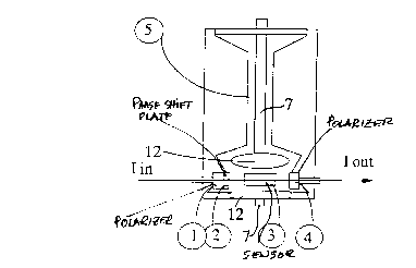
In Fig. 5 the basic components are inserted into the actual sensor. In addition, for
potential division the sensor is provided with capacitor 6 and wire 7 to lead the
measurement signal to crystal of the sensor 3. The inner space of the sensor is filled
with silicone 5. As an insulating material 9 of capacitor 6 favourably ceramics or
alternatively polypropylene is used. Conducting plates 16 of the capacitor 6 areformed onto the surface of ceramics 9. Particularly suitable ceramics for the
invention is the commercial product Makor having a dielectric constant ~ of 5.6.Using this embodiment a good voltage endurance and an appropriate resolution in
high frequency applications is achieved.
The embodiment according to Fig. 6 utilizes a symmetrical potential dividing on
both sides of crystal 3.
In the electric f1eld sensor according to Fig. 7 no potential dividing capacitor is
used, but the field is brought by wires 7 directly to the surface of crystal 3. The
whole sensor structure is surrounded by two semispherical conductive covers 7
* Registered trade mark
Wo s3tl2435 2 1 2 S ~ 3 5
pcr/Fl92/oo326
isolated from each other. The inner space of the sensor is filled with silicone 5.
The embodiment according to Fig. 8 corresponds the embodiment shown in Fig. 5
accomplished without potential dividing capacitor 6. The field is brought by wires 7
to metallizations 14 that are made directly on surface of crystal 3. The inner space
of the sensor is filled with silicone. Mesurements demonstrated that due to using
silicone the voltage endurance of the sensor improved approx. five times.
In the embodiment according to Fig. 9 the voltage being measured is brought by
wires 7 to conductive ball or plate 12 that is situated at a distance from crystal 3.
Rec~llse the inner structure is filled with silicone 5, the gap between plate 12 and
crystal 3 acts as a potential divider. The electric field is confined within silicone,
because silicone has a smaller dielectric constant than the crystal: ~ = 2.9 < ~c,yS~"
= 16. Silicone 5 has a high voltage endurance and also its extinction coefficient is
small, therefore silicone does not warm up even in an intensive high frequency
electric field.
The sensor according to Fig. 10 and 11 corresponds by its basic components to the
sensors shown in Fig. 4 - 9. The main difference is the prism 15 that returns the
light signal passed through crystal 3. As usually, there are polarizers 1 and 4 on the
path of the light, and phase shift plate 2 is on the path between the first polarizer 1
and crystal 3.
In the following, the properties of the significant components of the invention are
25 exemplified:
Crystal 3
Bi4Ge3012:
-43m-crystal symmetry; cubic,
-Refractive index n = 2,0975 (633 nm)
-Temperature dependence of refractive index (dn/dT)/n = 2- lO-~/K
(633 nm)
Wo 93/12435 21 2 5 3 3 5 pcr/Fl92/oo326
_
-Thermal coefficient of expansion (dH/dT)/h = 1 10~/K
-r4, = 0,95-10~'2m/V
-nO3r4, = 8,8-10~'2m/V (631 nm)
-Direction of the light path: [1-10]
S -Direction of the electric field: [110]
-On both [110]-surfaces of the crystal a chrome/(gold) film was
vaporized
-Dimensions of the crystal 3 x 7 x 10 mm
Phase shiR plate 2
-)~/4-phase shift plate
-Quartz
-Diameter S mm
-Thickness 3 mm or cube 3 x 3 x 3
Polarizers 1 and 4
Option 1 (the embodiment according to Fig. 10 - 11)
-Polarization cube
-Wave length: 830 nm
-Size: A = B = C = 5 mm
Option 2 (the embodiment according to Fig. 4 - 9)
-Polarization film
-Wave length: 830 nm
-Size: diameter 5 mm, thickness 1 mm.
Fibres 20:
Option I (Fig. 10- 11)
.
~ ~ ~r ~
-Ensign Pickfor~ *: HCP-M04 O OT- 10
-Diameter of the core 400 ~m
-Uncabled
Option 2 (Fig. 4 - 9)
-Ensign Pickford *: HCP-M02 O OT-AO 2VZ - O 7
-200/230,um (core/coating)
-Cabled; double cabled
Potential dividing capacitors
-ceramical material Makor or
-polypropene or
-teflon
-diameter 40 mm, height 10 - 60 mm
Case
-Case material: cast plastic with resin filling, ceramics or teflon tube
-The structure of the sensor was designed fully isolative
-Fibres were attached to the case by means of ceramic ferrules. The
ferrules were designed specially for this embodiment
-Selfoc*microlenses were placed into glass ceramic cartridges
-Components were placed into a v-groove
-The crystal was designed so that its natural vibrations were quickly
damped
-On the surfaces of the crystals chrome/gold films were vaporized
-As polarizers cube polarizers or film polarizers cut in an applopliate
size and shape were used
-Inner cavities of the sensors were filled with silicone (table 1)
In the following, a table is represented that illustrates properties of insulating
~, * Registered t rade mark
2125~95
- Wo 93/12435 pcr/Fl92/oo326
11
material 9 (glass ceramics) and silicone 5, applicable for the invention.
Table 1
Matenal Glass ceramics Silicone
(MACOR)
Type Sylgard 527
GENERAL PROPERTIES
density kg/m3 2520 970
ELECTRICAL
RESISTIVITY ohm-cm lE+14 2.3E+15
Extinction coefficient 0.003 0.00015
Dielectric constant 5.9 2.95
Voltage endurance kV/mm 40 17
HEAT
Thermal expansion ppm/K 10 990
Thermal conductivity W/mK 1.68
Minimum te"~,eldture (C) -65
Maximum ~e-"peldture (C) 1000 230
MECHANICAL
20 Modulus of elasticity GN/m2 65
Specific rigidity E/density 2.60E+07
OPTICAL
Refractive index n. 1.5
25 Instead of the infrared radiation mentioned in the examples above also other
wavelengths can be used in the invention.